Feature Summary
- 32-bit load/store RISC architecture
- Up to 15 general-purpose 32-bit registers
- 32-bit Stack Pointer, Program Counter, and Link Register reside in register file
- Fully orthogonal instruction set
- Pipelined architecture allows one instruction per clock cycle for most instructions
- Byte, half-word, word and double word memory access
- Fast interrupts and multiple interrupt priority levels
- Optional branch prediction for minimum delay branches
- Privileged and unprivileged modes enabling efficient and secure Operating Systems
- Innovative instruction set together with variable instruction length ensuring industry leading code density
- Optional DSP extention with saturated arithmetic, and a wide variety of multiply instructions
- Optional extensions for Java, SIMD, Read-Modify-Write to memory, and Coprocessors
- Architectural support for efficient On-Chip Debug solutions
- Optional MPU or MMU allows for advanced operating systems
- FlashVault™ support through Secure State for executing trusted code alongside nontrusted code on the same CPU

AVR32
Architecture Document
32000D-04/2011

1. Introduction
AVR32 is a new high-performance 32-bit RISC microprocessor core, designed for cost-sensitive embedded applications, with particular emphasis on low power consumption and high code density. In addition, the instruction set architecture has been tuned to allow for a variety of microarchitectures, enabling the AVR32 to be implemented as low-, mid- or high-performance processors. AVR32 extends the AVR family into the world of 32- and 64-bit applications.
1.1 The AVR family
The AVR family was launched by Atmel in 1996 and has had remarkable success in the 8- and 16-bit flash microcontroller market. AVR32 is complements the current AVR microcontrollers. Through the AVR32 family, the AVR is extended into a new range of higher performance applications that is currently served by 32- and 64-bit processors.
To truly exploit the power of a 32-bit architecture, the new AVR32 architecture is not binary compatible with earlier AVR architectures. In order to achieve high code density, the instruction format is flexible providing both compact instructions with 16 bits length and extended 32-bit instructions. While the instruction length is only 16 bits for most instructions, powerful 32-bit instructions are implemented to further increase performance. Compact and extended instructions can be freely mixed in the instruction stream.
1.2 The AVR32 Microprocessor Architecture
The AVR32 is a new innovative microprocessor architecture. It is a fully synchronous synthesizable RTL design with industry standard interfaces, ensuring easy integration into SoC designs with legacy intellectual property (IP). Through a quantitative approach, a large set of industry recognized benchmarks has been compiled and analyzed to achieve the best code density in its class of microprocessor architectures. In addition to lowering the memory requirements, a compact code size also contributes to the core’s low power characteristics. The processor supports byte and half-word data types without penalty in code size and performance.
Memory load and store operations are provided for byte, half-word, word and double word data with automatic sign- or zero extension of half-word and byte data. The C-compiler is closely linked to the architecture and is able to exploit code optimization features, both for size and speed.
In order to reduce code size to a minimum, some instructions have multiple addressing modes. As an example, instructions with immediates often have a compact format with a smaller immediate, and an extended format with a larger immediate. In this way, the compiler is able to use the format giving the smallest code size.
Another feature of the instruction set is that frequently used instructions, like add, have a compact format with two operands as well as an extended format with three operands. The larger format increases performance, allowing an addition and a data move in the same instruction in a single cycle.
Load and store instructions have several different formats in order to reduce code size and speed up execution:
- Load/store to an address specified by a pointer register
- Load/store to an address specified by a pointer register with postincrement
AVR32
- Load/store to an address specified by a pointer register with predecrement
- Load/store to an address specified by a pointer register with displacement
- Load/store to an address specified by a small immediate (direct addressing within a small page)
- Load/store to an address specified by a pointer register and an index register.
The register file is organized as 16 32-bit registers and includes the Program Counter, the Link Register, and the Stack Pointer. In addition, one register is designed to hold return values from function calls and is used implicitly by some instructions.
The AVR32 core defines several micro architectures in order to capture the entire range of applications. The microarchitectures are named AVR32A, AVR32B and so on. Different microarchitectures are suited to different end applications, allowing the designer to select a microarchitecture with the optimum set of parameters for a specific application.
1.2.1 Exceptions and Interrupts
The AVR32 incorporates a powerful exception handling scheme. The different exception sources, like Illegal Op-code and external interrupt requests, have different priority levels, ensuring a well-defined behavior when multiple exceptions are received simultaneously. Additionally, pending exceptions of a higher priority class may preempt handling of ongoing exceptions of a lower priority class. Each priority class has dedicated registers to keep the return address and status register thereby removing the need to perform time-consuming memory operations to save this information.
There are four levels of external interrupt requests, all executing in their own context. The contexts can provide a number of dedicated registers for the interrupts to use directly ensuring low latency. High priority interrupts may have a larger number of shadow registers available than low priority interrupts. An interrupt controller does the priority handling of the external interrupts and provides the prioritized interrupt vector to the processor core.
1.2.2 Java Support
Java hardware acceleration is available as an option, in the form of a Java Card or Java Virtual Machine hardware implementation.
1.2.3 FlashVault
Revision 3 of the AVR32 architecture introduced a new CPU state called Secure State. This state is instrumental in the new security technology named FlashVault. This innovation allows the on-chip flash and other memories to be partially programmed and locked, creating a safe on-chip storage for secret code and valuable software intellectual property. Code stored in the FlashVault will execute as normal, but reading, copying or debugging the code is not possible. This allows a device with FlashVault code protection to carry a piece of valuable software such as a math library or an encryption algorithm from a trusted location to a potentially untrustworthy partner where the rest of the source code can be developed, debugged and programmed.
32000D-04/2011 3
ATMEL
1.3 Microarchitectures
The AVR32 architecture defines different microarchitectures. This enables implementations that are tailored to specific needs and applications. The microarchitectures provide different performance levels at the expense of area and power consumption. The following microarchitectures are defined:
1.3.1 AVR32A
The AVR32A microarchitecture is targeted at cost-sensitive, lower-end applications like smaller microcontrollers. This microarchitecture does not provide dedicated hardware registers for shadowing of register file registers in interrupt contexts. Additionally, it does not provide hardware registers for the return address registers and return status registers. Instead, all this information is stored on the system stack. This saves chip area at the expense of slower interrupt handling.
Upon interrupt initiation, registers R8-R12 are automatically pushed to the system stack. These registers are pushed regardless of the priority level of the pending interrupt. The return address and status register are also automatically pushed to stack. The interrupt handler can therefore use R8-R12 freely. Upon interrupt completion, the old R8-R12 registers and status register are restored, and execution continues at the return address stored popped from stack.
The stack is also used to store the status register and return address for exceptions and scall. Executing the rete or rets instruction at the completion of an exception or system call will pop this status register and continue execution at the popped return address.
1.3.2 AVR32B
The AVR32B microarchitecture is targeted at applications where interrupt latency is important. The AVR32B therefore implements dedicated registers to hold the status register and return address for interrupts, exceptions and supervisor calls. This information does not need to be written to the stack, and latency is therefore reduced. Additionally, AVR32B allows hardware shadowing of the registers in the register file. The INT0 to INT3 contexts may have dedicated versions of the registers in the register file, allowing the interrupt routine to start executing immediately.
The scall, rete and rets instructions use the dedicated status register and return address registers in their operation. No stack accesses are performed.
4 AVR32 32000D-04/2011
AVR32
2. Programming Model
This chapter describes the programming model and the set of registers accessible to the user.
2.1 Data Formats
The AVR32 processor supports the data types shown in Table 2-1 on page 5:
Table 2-1. Overview of execution modes, their priorities and privilege levels.
When any of these types are described as unsigned, the N bit data value represents a non-negative integer in the range 0 to + $2^N$-1.
When any of these types are described as signed, the N bit data value represents an integer in the range of -$2^{N-1}$ to +$2^{N-1}$-1, using two's complement format.
Some instructions operate on fractional numbers. For these numbers, the data value represents a fraction in the range of -1 to +$1-2^{-(N-1)}$, using two's complement format.
2.2 Data Organization
Data is usually stored in a big-endian way, see Figure 2-1 on page 5. This means that when multi-byte data is stored in memory, the most significant byte is stored at the lowest address. All instructions are interpreted as being big-endian. However, in order to support data transfers that are little-endian, special endian-translating load and store instructions are defined.
The register file can hold data of different formats. Both byte, halfword (16-bit) and word (32-bit) formats can be represented, and byte and halfword formats are supported in both unsigned and signed 2's complement formats. Some instructions also use doubleword operands. Doubleword data are placed in two consecutive registers. The most significant word is in the uppermost register. Valid register pairs are R1:R0, R3:R2, R5:R4, R7:R6, R9:R8, R11:R10 and R13:R12.
Load and store operations that transfer bytes or halfwords, automatically zero-extends or signextends the bytes or half-words as they are loaded.
Figure 2-1. Data representation in the register file
AVR32 can access data of size byte, halfword, word and doubleword using dedicated instructions. The memory system can support unaligned accesses for selected load/store instructions in some implementations. Any other unaligned access will cause an address exception.
For performance reasons, the user should make sure that the stack always is word aligned. This means that only word instructions can be used to access the stack. When manipulating the stack pointer, the user has to ensure that the result is word aligned before trying to load and store data on the stack. Failing to do so will result in performance penalties. Code will execute correctly if the stack is unaligned but with a significant performance penalty.
2.3 Instruction Organization
The AVR32 instruction set has both compact and extended instructions. Compact instructions denotes the instructions which have a length of 16 bits while extended instructions have a length of 32 bits.
All instructions must be placed on halfword boundaries, see Table 2-2 on page 6. Extended instructions can be both aligned and unaligned to halfword boundaries. In normal instruction flow, the instruction buffer will always contain enough entries to ensure that compact, aligned extended and unaligned extended instructions can be issued in a single cycle.
Change-of-flow operations such as branches, jumps, calls and returns may in some implementations require the instruction buffer to be flushed. The user should consult the Technical Reference Manual for the specific implementation in order to determine how alignment of the branch target address affects performance.
Table 2-2. Instructions are stored in memory in a big endian fashion and must be aligned on half word boundaries
AVR32
2.4 Processor States
2.4.1 Normal RISC State
The AVR32 processor supports several different execution contexts as shown in Table 2-3 on page 7.
Table 2-3. Overview of execution modes, their priorities and privilege levels.
Mode changes can be made under software control, or can be caused by external interrupts or exception processing. A mode can be interrupted by a higher priority mode, but never by one with lower priority. Nested exceptions can be supported with a minimal software overhead.
When running an operating system on the AVR32, user processes will typically execute in the application mode. The programs executed in this mode are restricted from executing certain instructions. Furthermore, most system registers together with the upper halfword of the status register cannot be accessed. Protected memory areas are also not available. All other operating modes are privileged and are collectively called System Modes. They have full access to all privileged and unprivileged resources. After a reset, the processor will be in supervisor mode.
2.4.2 Debug State
The AVR32 can be set in a debug state, which allows implementation of software monitor routines that can read out and alter system information for use during application development. This implies that all system and application registers, including the status registers and program counters, are accessible in debug state. The privileged instructions are also available.
All interrupt levels are by default disabled when debug state is entered, but they can individually be switched on by the monitor routine by clearing the respective mask bit in the status register.
Debug state can be entered as described in the Technical Reference Manual.
Debug state is exited by the retd instruction.
2.4.3 Java State
Some versions of the AVR32 processor core comes with a Java Extension Module (JEM). The processor can be set in a Java State where normal RISC operations are suspended. The Java state is described in chapter 3.
2.4.4 Secure State
The secure state added in the AVR32 Architecture revision 3 allows executing secure or trusted software in alongside nonsecure or untrusted software on the same processor. Hardware mech-
anisms are in place to make sure the nonsecure software can not read or modify instruction or data belonging to the secure software. The secure state is described in chapter 4.
2.5 Entry and Exit Mechanism
Table 2-4 on page 8 illustrates how the different states and modes are entered and exited.
Table 2-4. Entry and exit from states, modes and functions
| Entry method | Exit method | |
|---|---|---|
| Non-maskable Interrupt | Signal on NMI line | rete |
| Exception Mode | Internal error signal generated | rete |
| Interrupt3 | Signal on INT3 line | rete |
| Interrupt2 | Signal on INT2 line | rete |
| Interrupt1 | Signal on INT1 line | rete |
| Interrupt0 | Signal on INT0 line | rete |
| Supervisor Mode | scall instruction | rets |
| Application Mode | Returned to from any of the above modes | Can not be exited from |
| Subprogram | Function call | ret{cond}, ldm, popm, mov PC, LR |
| Secure state | sscall | retss |
2.6 Register File
Each of AVR32’s normal operation modes described in Section 2.4.1 “Normal RISC State” on page 7 has a dedicated context. Note that the Stack Pointer (SP), Program Counter (PC) and the Link Register (LR) are mapped into the register file, making the effective register count for each context 13 general purpose registers. The mapping of SP, PC and LR allows ordinary instructions, like additions or subtractions, to use these registers. This results in efficient addressing of memory.
Register R12 is designed to hold return values from function calls, and the conditional return with move and test instruction use this register as an implicit return value operand. The load multiple and pop multiple instructions have the same functionality, which enables them to be used as return instructions.
The AVR32 core’s orthogonal instruction set allows all registers in the register file to be used as pointers.
2.6.1 Register file in AVR32A
The AVR32A is targeted for cost-sensitive applications. Therefore, no hardware-shadowing of registers is provided, see Figure 2-2 on page 9. All data that must be saved between execution states are placed on the system stack, not in dedicated registers as done in AVR32B. A shadowed stack pointer is still provided for the privileged modes, facilitating a dedicated system stack.
When an exception occurs in an AVR32A-compliant implementation, the status register and return address are pushed by hardware onto the system stack. When an INT0, INT1, INT2 or INT3 occurs, the status register, return address, R8-R12 and LR are pushed on the system stack. The corresponding registers are popped from stack by the rete instruction. The scall and rets instructions also use the system stack to store the return address and status register.
8 AVR32 32000D–□□/□□□□
AVR32
Figure 2-2. Register File in AVR32A
| Application | Supervisor | INT0 | INT1 | INT2 | INT3 | Exception | NMI |
|---|---|---|---|---|---|---|---|
| Bit 31 Bit 0 | Bit 31 Bit 0 | Bit 31 Bit 0 | Bit 31 Bit 0 | Bit 31 Bit 0 | Bit 31 Bit 0 | Bit 31 Bit 0 | Bit 31 Bit 0 |
| PC | PC | PC | PC | PC | PC | PC | PC |
| LR | LR | LR | LR | LR | LR | LR | LR |
| SP_APP | SP_SYS | SP_SYS | SP_SYS | SP_SYS | SP_SYS | SP_SYS | SP_SYS |
| R12 | R12 | R12 | R12 | R12 | R12 | R12 | R12 |
| R11 | R11 | R11 | R11 | R11 | R11 | R11 | R11 |
| R10 | R10 | R10 | R10 | R10 | R10 | R10 | R10 |
| R9 | R9 | R9 | R9 | R9 | R9 | R9 | R9 |
| R8 | R8 | R8 | R8 | R8 | R8 | R8 | R8 |
| R7 | R7 | R7 | R7 | R7 | R7 | R7 | R7 |
| R6 | R6 | R6 | R6 | R6 | R6 | R6 | R6 |
| R5 | R5 | R5 | R5 | R5 | R5 | R5 | R5 |
| R4 | R4 | R4 | R4 | R4 | R4 | R4 | R4 |
| R3 | R3 | R3 | R3 | R3 | R3 | R3 | R3 |
| R2 | R2 | R2 | R2 | R2 | R2 | R2 | R2 |
| R1 | R1 | R1 | R1 | R1 | R1 | R1 | R1 |
| R0 | R0 | R0 | R0 | R0 | R0 | R0 | R0 |
| SR | SR | SR | SR | SR | SR | SR | SR |
2.6.2 Register File in AVR32B
The AVR32B allows separate register files for the interrupt and exception modes, see Figure 2-3 on page 9. These modes have a number of implementation defined shadowed registers in order to speed up interrupt handling. The shadowed registers are automatically mapped in depending on the current execution mode.
All contexts, except Application, have a dedicated Return Status Register (RSR) and Return Address Register (RAR). The RSR registers are used for storing the Status Register value in the context to return to. The RAR registers are used for storing the address in the context to return to. The RSR and RAR registers eliminates the need to temporarily store the Status Register and return address to stack when entering a new context.
Figure 2-3. Register File in AVR32B
| Application | Supervisor | INT0 | INT1 | INT2 | INT3 | Exception | NMI |
|---|---|---|---|---|---|---|---|
| Bit 31 Bit 0 | Bit 31 Bit 0 | Bit 31 Bit 0 | Bit 31 Bit 0 | Bit 31 Bit 0 | Bit 31 Bit 0 | Bit 31 Bit 0 | Bit 31 Bit 0 |
| PC | PC | PC | PC | PC | PC | PC | PC |
| LR | LR | LR / LR_INT0 | LR / LR_INT1 | LR / LR_INT2 | LR / LR_INT3 | LR | LR |
| SP_APP | SP_SYS | SP_SYS | SP_SYS | SP_SYS | SP_SYS | SP_SYS | SP_SYS |
| R12 | R12 | R12 | R12 | ||||
| R11 | R11 | R11 | R11 | ||||
| R10 | R10 | R10 | R10 | ||||
| R9 | R9 | R9 | R9 | ||||
| R8 | R8 | R8 | R8 | ||||
| R7 | R7 | R7 | R7 | ||||
| R6 | R6 | R6 | R6 | ||||
| R5 | R5 | R5 | R5 | ||||
| R4 | R4 | R4 | R4 | ||||
| R3 | R3 | R3 | R3 | ||||
| R2 | R2 | R2 | R2 | ||||
| R1 | R1 | R1 | R1 | ||||
| R0 | R0 | R0 | R0 | ||||
| SR | SR | SR | SR | SR | SR | SR | SR |
| RSR_SUP | RSR_INT0 | RSR_INT1 | RSR_INT2 | RSR_INT3 | RSR_EX | RSR_NMI | |
| RAR_SUP | RAR_INT0 | RAR_INT1 | RAR_INT2 | RAR_INT3 | RAR_EX | RAR_NMI |
The register file is designed with an implementation specific part and an architectural defined part. Depending on the implementation, each of the interrupt modes can have different configu-
32000D–□□/□□□□
9
rations of shadowed registers. This allows for maximum flexibility in targeting the processor for different application, see Figure 2-4 on page 10.
Figure 2-4. A typical AVR32B register file implementation
| Application | Supervisor | INT0 | INT1 | INT2 | INT3 | Exception | NMI |
|---|---|---|---|---|---|---|---|
| Bit 31 Bit 0 | Bit 31 Bit 0 | Bit 31 Bit 0 | Bit 31 Bit 0 | Bit 31 Bit 0 | Bit 31 Bit 0 | Bit 31 Bit 0 | Bit 31 Bit 0 |
| PC | PC | PC | PC | PC | PC | PC | PC |
| LR | LR | LR | LR | LR_INT2 | LR_INT3 | LR | LR |
| SP_APP | SP_SYS | SP_SYS | SP_SYS | SP_SYS | SP_SYS | SP_SYS | SP_SYS |
| R12 | R12 | R12 | R12 | R12_INT2 | R12_INT3 | R12 | R12 |
| R11 | R11 | R11 | R11 | R11_INT2 | R11_INT3 | R11 | R11 |
| R10 | R10 | R10 | R10 | R10_INT2 | R10_INT3 | R10 | R10 |
| R9 | R9 | R9 | R9 | R9_INT2 | R9_INT3 | R9 | R9 |
| R8 | R8 | R8 | R8 | R8_INT2 | R8_INT3 | R8 | R8 |
| R7 | R7 | R7 | R7 | R7 | R7_INT3 | R7 | R7 |
| R6 | R6 | R6 | R6 | R6 | R6_INT3 | R6 | R6 |
| R5 | R5 | R5 | R5 | R5 | R5_INT3 | R5 | R5 |
| R4 | R4 | R4 | R4 | R4 | R4_INT3 | R4 | R4 |
| R3 | R3 | R3 | R3 | R3 | R3_INT3 | R3 | R3 |
| R2 | R2 | R2 | R2 | R2 | R2_INT3 | R2 | R2 |
| R1 | R1 | R1 | R1 | R1 | R1_INT3 | R1 | R1 |
| R0 | R0 | R0 | R0 | R0 | R0_INT3 | R0 | R0 |
| SR | SR | SR | SR | SR | SR | SR | SR |
| RSR_SUP | RSR_INT0 | RSR_INT1 | RSR_INT2 | RSR_INT3 | RSR_EX | RSR_NMI | |
| RAR_SUP | RAR_INT0 | RAR_INT1 | RAR_INT2 | RAR_INT3 | RAR_EX | RAR_NMI |
Three different shadowing schemes are offered, small, half and full, ranging from no general registers shadowed to all general registers shadowed, see Figure 2-5 on page 10.
Figure 2-5. AVR32 offers three different models for shadowed registers.
| Small | Half | Full |
|---|---|---|
| Bit 31 Bit 0 | Bit 31 Bit 0 | Bit 31 Bit 0 |
| PC | PC | PC |
| LR | LR_INTx | LR_INTx |
| SP_SYS | SP_SYS | SP_SYS |
| R12 | R12_INTx | R12_INTx |
| R11 | R11_INTx | R11_INTx |
| R10 | R10_INTx | R10_INTx |
| R9 | R9_INTx | R9_INTx |
| R8 | R8_INTx | R8_INTx |
| R7 | R7 | R7_INTx |
| R6 | R6 | R6_INTx |
| R5 | R5 | R5_INTx |
| R4 | R4 | R4_INTx |
| R3 | R3 | R3_INTx |
| R2 | R2 | R2_INTx |
| R1 | R1 | R1_INTx |
| R0 | R0 | R0_INTx |
2.7 The Stack Pointer
Since the Stack Pointer (SP) is located in the register file, it can be addressed as an ordinary register. This simplifies allocation and access of local variables and parameters. The Stack Pointer is also used implicitly by several instructions.
The system modes have a shadowed stack pointer different from the application mode stack pointer. This allows having a separate system stack.
2.8 The Program Counter
The Program Counter (PC) contains the address of the instruction being executed. The memory space is byte addressed. With the exception of Java state, the instruction size is a multiple of 2 bytes and the LSB of the Program Counter is fixed to zero. The PC is automatically incremented in normal program flow, depending on the size of the current instruction.
The PC is mapped into the register file and it can be used as a source or destination operand in all instructions using register operands. This includes arithmetical or logical instructions and load/store instructions. Instructions using PC as destination register are treated the same way as jump instructions. This implies that the pipeline is flushed, and execution resumed at the address specified by the new PC value.
2.9 The Link Register
The general purpose register R14 is used as a Link Register in all modes. The Link Register holds subroutine return addresses. When a subroutine call is performed by a variant of the call instruction, LR is set to hold the subroutine return address. The subroutine return is performed by copying LR back to the program counter, either explicitly by a mov instruction, by using a ldm or popm instruction or a ret instruction.
The Link Register R14 can be used as a general-purpose register at all other times.
2.10 The Status Register
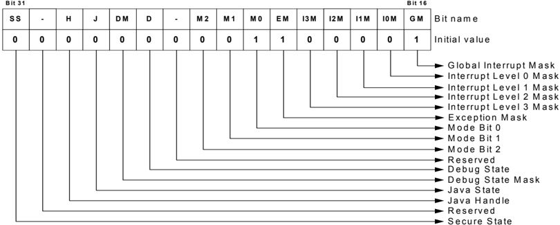
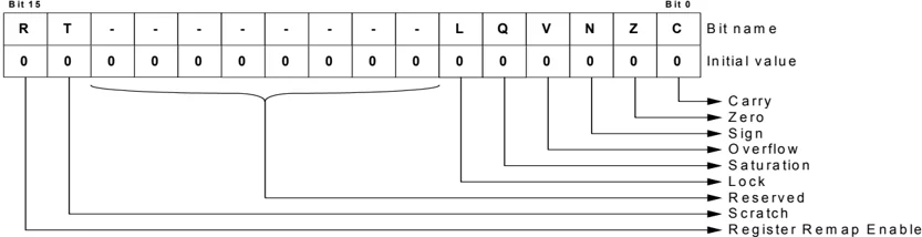
The Status Register (SR) is split into two halfwords, one upper and one lower, see Figure 2-6 on page 11 and Figure 2-7 on page 12. The lower halfword contains the C, Z, N, V and Q flags, while the upper halfword contains information about the mode and state the processor executes in. The upper halfword can only be accessed from a privileged mode.
Figure 2-6. The Status Register high halfword
32000D–□□/□□□□ ATMEL® 11
Figure 2-7. The Status Register low halfword
SS - Secure State This bit is indicates if the processor is executing in the secure state. For more details, see chapter 4. The bit is initialized in an IMPLEMENTATION DEFINED way at reset.
H - Java Handle This bit is included to support different heap types in the Java Virtual Machine. For more details, see chapter 3. The bit is cleared at reset.
J - Java State The processor is in Java state when this bit is set. The incoming instruction stream will be decoded as a stream of Java bytecodes, not RISC opcodes. The bit is cleared at reset. This bit should not be modified by the user as undefined behaviour may result.
DM - Debug State Mask If this bit is set, the Debug State is masked and cannot be entered. The bit is cleared at reset, and can both be read and written by software.
D - Debug State The processor is in debug state when this bit is set. The bit is cleared at reset and should only be modified by debug hardware, the breakpoint instruction or the retd instruction. Undefined behaviour may result if the user tries to modify this bit manually.
M2, M1, M0 - Execution Mode These bits show the active execution mode. The settings for the different modes are shown in Table 2-5 on page 13. M2 and M1 are cleared by reset while M0 is set so that the processor is in supervisor mode after reset. These bits are modified by hardware, or execution of certain instructions like scall, rets and rete. Undefined behaviour may result if the user tries to modify these bits manually.
12 AVR32 32000D–04/2011
Table 2-5. Mode bit settings
| M2 | M1 | M0 | Mode |
|---|---|---|---|
| 1 | 1 | 1 | Non Maskable Interrupt |
| 1 | 1 | 0 | Exception |
| 1 | 0 | 1 | Interrupt level 3 |
| 1 | 0 | 0 | Interrupt level 2 |
| 0 | 1 | 1 | Interrupt level 1 |
| 0 | 1 | 0 | Interrupt level 0 |
| 0 | 0 | 1 | Supervisor |
| 0 | 0 | 0 | Application |
EM - Exception mask
When this bit is set, exceptions are masked. Exceptions are enabled otherwise. The bit is automatically set when exception processing is initiated or Debug Mode is entered. Software may clear this bit after performing the necessary measures if nested exceptions should be supported. This bit is set at reset.
I3M - Interrupt level 3 mask
When this bit is set, level 3 interrupts are masked. If I3M and GM are cleared, INT3 interrupts are enabled. The bit is automatically set when INT3 processing is initiated. Software may clear this bit after performing the necessary measures if nested INT3s should be supported. This bit is cleared at reset.
I2M - Interrupt level 2 mask
When this bit is set, level 2 interrupts are masked. If I2M and GM are cleared, INT2 interrupts are enabled. The bit is automatically set when INT3 or INT2 processing is initiated. Software may clear this bit after performing the necessary measures if nested INT2s should be supported. This bit is cleared at reset.
I1M - Interrupt level 1 mask
When this bit is set, level 1 interrupts are masked. If I1M and GM are cleared, INT1 interrupts are enabled. The bit is automatically set when INT3, INT2 or INT1 processing is initiated. Software may clear this bit after performing the necessary measures if nested INT1s should be supported. This bit is cleared at reset.
I0M - Interrupt level 0 mask
When this bit is set, level 0 interrupts are masked. If I0M and GM are cleared, INT0 interrupts are enabled. The bit is automatically set when INT3, INT2, INT1 or INT0 processing is initiated. Software may clear this bit after performing the necessary measures if nested INT0s should be supported. This bit is cleared at reset.
GM - Global Interrupt Mask
When this bit is set, all interrupts are disabled. This bit overrides I0M, I1M, I2M and I3M. The bit is automatically set when exception processing is initiated, Debug Mode is entered, or a Java trap is taken. This bit is automatically cleared when returning from a Java trap. This bit is set after reset.
32000D–□□/□□□□
13
R - Java register remap When this bit is set, the addresses of the registers in the register file is dynamically changed. This allows efficient use of the register file registers as a stack. For more details, see chapter 3.. The R bit is cleared at reset. Undefined behaviour may result if this bit is modified by the user.
T - Scratch bit This bit is not set or cleared implicit by any instruction and the programmer can therefore use this bit as a custom flag to for example signal events in the program. This bit is cleared at reset.
L - Lock flag Used by the conditional store instruction. Used to support atomical memory access. Automatically cleared by rete. This bit is cleared after reset.
Q - Saturation flag The saturation flag indicates that a saturating arithmetic operation overflowed. The flag is sticky and once set it has to be manually cleared by a csrf instruction after the desired action has been taken. See the Instruction set description for details.
V - Overflow flag The overflow flag indicates that an arithmetic operation overflowed. See the Instruction set description for details.
N - Negative flag The negative flag is modified by arithmetical and logical operations. See the Instruction set description for details.
Z - Zero flag The zero flag indicates a zero result after an arithmetic or logic operation. See the Instruction set description for details.
C - Carry flag The carry flag indicates a carry after an arithmetic or logic operation. See the Instruction set description for details.
2.11 System registers
The system registers are placed outside of the virtual memory space, and are only accessible using the privileged mfsr and mtsr instructions, see Table 2-7 on page 15. The number of physical locations is IMPLEMENTATION DEFINED, but a maximum of 256 locations can be addressed with the dedicated instructions. Some of the System Registers are altered automatically by hardware.
The reset value of the System Registers are IMPLEMENTATION DEFINED.
14 AVR32 32000D–04/2011
The Compliance column describes if the register is Required, Optional or Unused in AVR32A and AVR32B, see Table 2-6 on page 15 for legend.
Table 2-6. Legend for the Compliance column
| Abbreviation | Meaning |
|---|---|
| RA | Required in AVR32A |
| OA | Optional in AVR32A |
| UA | Unused in AVR32A |
| RB | Required in AVR32B |
| OB | Optional in AVR32B |
| UB | Unused in AVR32B |
Table 2-7. System Registers
| Reg # | Address | Name | Function | Compliance | |
|---|---|---|---|---|---|
| 0 | 0 | SR | Status Register | RA | RB |
| 1 | 4 | EVBA | Exception Vector Base Address | RA | RB |
| 2 | 8 | ACBA | Application Call Base Address | RA | RB |
| 3 | 12 | CPUCR | CPU Control Register | RA | RB |
| 4 | 16 | ECR | Exception Cause Register | OA | OB |
| 5 | 20 | RSR_SUP | Return Status Register for Supervisor context | UA | RB |
| 6 | 24 | RSR_INT0 | Return Status Register for INT 0 context | UA | RB |
| 7 | 28 | RSR_INT1 | Return Status Register for INT 1 context | UA | RB |
| 8 | 32 | RSR_INT2 | Return Status Register for INT 2 context | UA | RB |
| 9 | 36 | RSR_INT3 | Return Status Register for INT 3 context | UA | RB |
| 10 | 40 | RSR_EX | Return Status Register for Exception context | UA | RB |
| 11 | 44 | RSR_NMI | Return Status Register for NMI context | UA | RB |
| 12 | 48 | RSR_DBG | Return Status Register for Debug Mode | OA | OB |
| 13 | 52 | RAR_SUP | Return Address Register for Supervisor context | UA | RB |
| 14 | 56 | RAR_INT0 | Return Address Register for INT 0 context | UA | RB |
| 15 | 60 | RAR_INT1 | Return Address Register for INT 1 context | UA | RB |
| 16 | 64 | RAR_INT2 | Return Address Register for INT 2 context | UA | RB |
| 17 | 68 | RAR_INT3 | Return Address Register for INT 3 context | UA | RB |
| 18 | 72 | RAR_EX | Return Address Register for Exception context | UA | RB |
| 19 | 76 | RAR_NMI | Return Address Register for NMI context | UA | RB |
| 20 | 80 | RAR_DBG | Return Address Register for Debug Mode | OA | OB |
| 21 | 84 | JECR | Java Exception Cause Register | OA | OB |
| 22 | 88 | JOSP | Java Operand Stack Pointer | OA | OB |
| 23 | 92 | JAVA_LV0 | Java Local Variable 0 | OA | OB |
Table 2-7. System Registers (Continued)
| Reg # | Address | Name | Function | Compliance | |
|---|---|---|---|---|---|
| 24 | 96 | JAVA_LV1 | Java Local Variable 1 | OA | OB |
| 25 | 100 | JAVA_LV2 | Java Local Variable 2 | OA | OB |
| 26 | 104 | JAVA_LV3 | Java Local Variable 3 | OA | OB |
| 27 | 108 | JAVA_LV4 | Java Local Variable 4 | OA | OB |
| 28 | 112 | JAVA_LV5 | Java Local Variable 5 | OA | OB |
| 29 | 116 | JAVA_LV6 | Java Local Variable 6 | OA | OB |
| 30 | 120 | JAVA_LV7 | Java Local Variable 7 | OA | OB |
| 31 | 124 | JTBA | Java Trap Base Address | OA | OB |
| 32 | 128 | JBCR | Java Write Barrier Control Register | OA | OB |
| 33-63 | 132-252 | Reserved | Reserved for future use | - | - |
| 64 | 256 | CONFIG0 | Configuration register 0 | RA | RB |
| 65 | 260 | CONFIG1 | Configuration register 1 | RA | RB |
| 66 | 264 | COUNT | Cycle Counter register | RA | RB |
| 67 | 268 | COMPARE | Compare register | RA | RB |
| 68 | 272 | TLBEHI | MMU TLB Entry High | OA | OB |
| 69 | 276 | TLBELO | MMU TLB Entry Low | OA | OB |
| 70 | 280 | PTBR | MMU Page Table Base Register | OA | OB |
| 71 | 284 | TLBEAR | MMU TLB Exception Address Register | OA | OB |
| 72 | 288 | MMUCR | MMU Control Register | OA | OB |
| 73 | 292 | TLBARLO | MMU TLB Accessed Register Low | OA | OB |
| 74 | 296 | TLBARHI | MMU TLB Accessed Register High | OA | OB |
| 75 | 300 | PCCNT | Performance Clock Counter | OA | OB |
| 76 | 304 | PCNT0 | Performance Counter 0 | OA | OB |
| 77 | 308 | PCNT1 | Performance Counter 1 | OA | OB |
| 78 | 312 | PCCR | Performance Counter Control Register | OA | OB |
| 79 | 316 | BEAR | Bus Error Address Register | OA | OB |
| 80 | 320 | MPUAR0 | MPU Address Register region 0 | OA | OB |
| 81 | 324 | MPUAR1 | MPU Address Register region 1 | OA | OB |
| 82 | 328 | MPUAR2 | MPU Address Register region 2 | OA | OB |
| 83 | 332 | MPUAR3 | MPU Address Register region 3 | OA | OB |
| 84 | 336 | MPUAR4 | MPU Address Register region 4 | OA | OB |
| 85 | 340 | MPUAR5 | MPU Address Register region 5 | OA | OB |
| 86 | 344 | MPUAR6 | MPU Address Register region 6 | OA | OB |
| 87 | 348 | MPUAR7 | MPU Address Register region 7 | OA | OB |
| 88 | 352 | MPUPSR0 | MPU Privilege Select Register region 0 | OA | OB |
| 89 | 356 | MPUPSR1 | MPU Privilege Select Register region 1 | OA | OB |
16 AVR32 32000D–04/2011
AVR32
Table 2-7. System Registers (Continued)
| Reg # | Address | Name | Function | Compliance | |
|---|---|---|---|---|---|
| 90 | 360 | MPUPSR2 | MPU Privilege Select Register region 2 | OA | OB |
| 91 | 364 | MPUPSR3 | MPU Privilege Select Register region 3 | OA | OB |
| 92 | 368 | MPUPSR4 | MPU Privilege Select Register region 4 | OA | OB |
| 93 | 372 | MPUPSR5 | MPU Privilege Select Register region 5 | OA | OB |
| 94 | 376 | MPUPSR6 | MPU Privilege Select Register region 6 | OA | OB |
| 95 | 380 | MPUPSR7 | MPU Privilege Select Register region 7 | OA | OB |
| 96 | 384 | MPUCRA | MPU Cacheable Register A | OA | OB |
| 97 | 388 | MPUCRB | MPU Cacheable Register B | OA | OB |
| 98 | 392 | MPUBRA | MPU Bufferable Register A | OA | OB |
| 99 | 396 | MPUBRB | MPU Bufferable Register B | OA | OB |
| 100 | 400 | MPUAPRA | MPU Access Permission Register A | OA | OB |
| 101 | 404 | MPUAPRB | MPU Access Permission Register B | OA | OB |
| 102 | 408 | MPUCR | MPU Control Register | OA | OB |
| 103 | 412 | SS_STATUS | Secure State Status Register | OA | OB |
| 104 | 416 | SS_ADRF | Secure State Address Flash Register | OA | OB |
| 105 | 420 | SS_ADRR | Secure State Address RAM Register | OA | OB |
| 106 | 424 | SS_ADR0 | Secure State Address 0 Register | OA | OB |
| 107 | 428 | SS_ADR1 | Secure State Address 1 Register | OA | OB |
| 108 | 432 | SS_SP_SYS | Secure State Stack Pointer System Register | OA | OB |
| 109 | 436 | SS_SP_APP | Secure State Stack Pointer Application Register | OA | OB |
| 110 | 440 | SS_RAR | Secure State Return Address Register | OA | OB |
| 111 | 444 | SS_RSR | Secure State Return Status Register | OA | OB |
| 112-191 | 448-764 | Reserved | Reserved for future use | - | - |
| 192-255 | 768-1020 | IMPL | IMPLEMENTATION DEFINED | - | - |
SR- Status Register
The Status Register is mapped into the system register space. This allows it to be loaded into the register file to be modified, or to be stored to memory. The Status Register is described in detail in Section 2.10 “The Status Register” on page 11.
EVBA - Exception Vector Base Address
This register contains a pointer to the exception routines. All exception routines start at this address, or at a defined offset relative to the address. Special alignment requirements may apply for EVBA, depending on the implementation of the interrupt controller. Exceptions are described in detail in Section 8. “Event Processing” on page 63.
ACBA - Application Call Base Address
Pointer to the start of a table of function pointers. Subroutines can thereby be called by the compact acall instruction. This facilitates efficient reuse of code. Keeping this pointer as a register facilitates multiple function pointer tables. ACBA is a full 32 bit register, but the lowest two bits
32000D–□□/□□□□
should be written to zero, making ACBA word aligned. Failing to do so may result in erroneous behaviour.
CPUCR - CPU Control Register Register controlling the configuration and behaviour of the CPU. The behaviour of this register is IMPLEMENTATION DEFINED. An example of a typical control bit in the CPUCR is an enable bit for branch prediction.
ECR - Exception Cause Register This register identifies the cause of the most recently executed exception. This information may be used to handle exceptions more efficiently in certain operating systems. The register is updated with a value equal to the EVBA offset of the exception, shifted 2 bit positions to the right. Only the 9 lowest bits of the EVBA offset are considered. As an example, an ITLB miss jumps to EVBA+0x50. The ECR will then be loaded with 0x50>>2 == 0x14. The ECR register is not loaded when an scall, Breakpoint or OCD Stop CPU exception is taken. Note that for interrupts, the offset is given by the autovector provided by the interrupt controller. The resulting ECR value may therefore overlap with an ECR value used by a regular exception. This can be avoided by choosing the autovector offsets so that no such overlaps occur.
RSR_SUP, RSR_INT0, RSR_INT1, RSR_INT2, RSR_INT3, RSR_EX, RSR_NMI - Return Status Registers If a request for a mode change, for instance an interrupt request, is accepted when executing in a context C, the Status Register values in context C are automatically stored in the Return Status Register (RSR) associated with the interrupt context I. When the execution in the interrupt state I is finished and the rets / rete instruction is encountered, the RSR associated with I is copied to SR, and the execution continues in the original context C.
RSR_DBG - Return Status Register for Debug Mode When Debug mode is entered, the status register contents of the original mode is automatically saved in this register. When the debug routine is finished, the retd instruction copies the contents of RSR_DBG into SR.
RAR_SUP, RAR_INT0, RAR_INT1, RAR_INT2, RAR_INT3, RAR_EX, RAR_NMI - Return Address Registers If a request for a mode change, for instance an interrupt request, is accepted when executing in a context C, the re-entry address of context C is automatically stored in the Return Address Register (RAR) associated with the interrupt context I. When the execution in the interrupt state I is finished and the rets / rete instruction is encountered, a change-of-flow to the address in the RAR associated with I, and the execution continues in the original context C. The calculation of the re-entry addresses is described in Section 8. "Event Processing" on page 63.
RAR_DBG - Return Address Register for Debug Mode When Debug mode is entered, the Program Counter contents of the original mode is automatically saved in this register. When the debug routine is finished, the retd instruction copies the contents of RAR_DBG into PC.
JECR - Java Exception Cause Register This register contains information needed for Java traps, see AVR32 Java Technical Reference Manual for details.
JOSP - Java Operand Stack Pointer This register holds the Java Operand Stack Pointer. The register is initialized to 0 at reset.
18 AVR32 32000D-04/2011
AVR32
JAVA_LVx - Java Local Variable Registers The Java Extension Module uses these registers to store local variables temporary.
JTBA - Java Trap Base Address This register contains the base address to the program code for the trapped Java instructions.
JBCR - Java Write Barrier Control Register This register is used by the garbage collector in the Java Virtual Machine.
CONFIG0 / 1 - Configuration Register 0 / 1 Used to describe the processor, its configuration and capabilities. The contents and functionality of these registers is described in detail in Section 2.11.1 “Configuration Registers” on page 21.
COUNT - Cycle Counter Register The COUNT register increments once every clock cycle, regardless of pipeline stalls and flushes. The COUNT register can both be read and written. The count register can be used together with the COMPARE register to create a timer with interrupt functionality. The COUNT register is written to zero upon reset and compare match. Revision 3 of the AVR32 Architecture allows some implementations to disable this automatic clearing of COUNT upon COMPARE match, usually by programming a bit in CPUCR. Refer to the Technical Reference Manual for the device for details. Incrementation of the COUNT register can not be disabled. The COUNT register will increment even though a compare interrupt is pending.
COMPARE - Cycle Counter Compare Register The COMPARE register holds a value that the COUNT register is compared against. The COMPARE register can both be read and written. When the COMPARE and COUNT registers match, a compare interrupt request is generated and COUNT is reset to 0. This interrupt request is routed out to the interrupt controller, which may forward the request back to the processor as a normal interrupt request at a priority level determined by the interrupt controller. Writing a value to the COMPARE register clears any pending compare interrupt requests. The compare and exception generation feature is disabled if the COMPARE register contains the value zero. The COMPARE register is written to zero upon reset.
TLBEHI - MMU TLB Entry Register High Part Used to interface the CPU to the TLB. The contents and functionality of the register is described in detail in Section 5. “Memory Management Unit” on page 35.
TLBELO - MMU TLB Entry Register Low Part Used to interface the CPU to the TLB. The contents and functionality of the register is described in detail in Section 5. “Memory Management Unit” on page 35.
PTBR - MMU Page Table Base Register Contains a pointer to the start of the Page Table. The contents and functionality of the register is described in detail in Section 5. “Memory Management Unit” on page 35.
TLBEAR - MMU TLB Exception Address Register Contains the virtual address that caused the most recent MMU error. The contents and functionality of the register is described in detail in Section 5. “Memory Management Unit” on page 35.
32000D–04/2011 19
ATMEL
MMUCR - MMU Control Register Used to control the MMU and the TLB. The contents and functionality of the register is described in detail in Section 5. “Memory Management Unit” on page 35.
TLBARLO / TLBARHI - MMU TLB Accessed Register Low / High Contains the Accessed bits for the TLB. The contents and functionality of the register is described in detail in Section 5. “Memory Management Unit” on page 35.
PCCNT - Performance Clock Counter Clock cycle counter for performance counters. The contents and functionality of the register is described in detail in Section 7. “Performance counters” on page 57.
PCNT0 / PCNT1 - Performance Counter 0 / 1 Counts the events specified by the Performance Counter Control Register. The contents and functionality of the register is described in detail in Section 7. “Performance counters” on page 57.
PCCR - Performance Counter Control Register Controls and configures the setup of the performance counters. The contents and functionality of the register is described in detail in Section 7. “Performance counters” on page 57.
BEAR - Bus Error Address Register Physical address that caused a Data Bus Error. This register is Read Only. Writes are allowed, but are ignored.
MPUARn - MPU Address Register n Registers that define the base address and size of the protection regions. Refer to Section 6. “Memory Protection Unit” on page 51 for details.
MPUPSRn - MPU Privilege Select Register n Registers that define which privilege register set to use for the different subregions in each protection region. Refer to Section 6. “Memory Protection Unit” on page 51 for details.
MPUCRA / MPUCRB - MPU Cacheable Register A / B Registers that define if the different protection regions are cacheable. Refer to Section 6. “Memory Protection Unit” on page 51 for details.
MPUBRA / MPUBRB - MPU Bufferable Register A / B Registers that define if the different protection regions are bufferable. Refer to Section 6. “Memory Protection Unit” on page 51 for details.
MPUAPRA / MPUAPRB - MPU Access Permission Register A / B Registers that define the access permissions for the different protection regions. Refer to Section 6. “Memory Protection Unit” on page 51 for details.
MPUCR - MPU Control Register Register that control the operation of the MPU. Refer to Section 6. “Memory Protection Unit” on page 51 for details.
20 AVR32 32000D–04/2011
SS_STATUS - Secure State Status Register Register that can be used to pass status or other information from the secure state to the nonsecure state. Refer to Section 4. “Secure state” on page 31 for details.
SS_ADRF, SS_ADRR, SS_ADR0, SS_ADR1 - Secure State Address Registers Registers used to partition memories into a secure and a nonsecure section. Refer to Section 4. “Secure state” on page 31 for details.
SS_SP_SYS, SS_SP_APP - Secure State SP_SYS and SP_APP Registers Read-only registers containing the SP_SYS and SP_APP values. Refer to Section 4. “Secure state” on page 31 for details.
SS_RAR, SS_RSR - Secure State Return Address and Return Status Registers Contains the address and status register of the sscall instruction that called secure state. Also used when returning to nonsecure state with the retss instruction. Refer to Section 4. “Secure state” on page 31 for details.
2.11.1 Configuration Registers Configuration registers are used to inform applications and operating systems about the setup and configuration of the processor on which it is running, see Figure 2-8 on page 21. The AVR32 implements the following read-only configuration registers.
Figure 2-8. Configuration Registers
CONFIG0
\begin{tabular}{|c|c|c|c|c|c|c|c|c|c|c|c|c|c|c|c|} \hline \multicolumn{1}{|c|}{31} & \multicolumn{1}{c|}{24} & 23 & \multicolumn{1}{c|}{20} & 19 & \multicolumn{1}{c|}{16} & 15 & \multicolumn{1}{c|}{13} & 12 & \multicolumn{1}{c|}{10} & 9 & \multicolumn{1}{c|}{7} & 6 & 5 & 4 & \multicolumn{1}{c|}{3} & 2 & 1 & 0 \ \hline Processor ID & \multicolumn{3}{c|}{-} & Processor Revision & \multicolumn{2}{c|}{AT} & \multicolumn{2}{c|}{AR} & \multicolumn{2}{c|}{MMUT} & F & J & P & O & S & D & R \ \hline \end{tabular}
CONFIG1
\begin{tabular}{|c|c|c|c|c|c|c|c|} \hline \multicolumn{1}{|c|}{31} & \multicolumn{1}{c|}{26} & 25 & \multicolumn{1}{c|}{20} & 19 & \multicolumn{1}{c|}{16} & 15 & \multicolumn{1}{c|}{13} & 12 & \multicolumn{1}{c|}{10} & 9 & \multicolumn{1}{c|}{6} & 5 & \multicolumn{1}{c|}{3} & 2 & 0 \ \hline IMMU SZ & \multicolumn{2}{c|}{DMMU SZ} & \multicolumn{2}{c|}{ISET} & \multicolumn{2}{c|}{ILSZ} & \multicolumn{2}{c|}{IASS} & \multicolumn{2}{c|}{DSET} & \multicolumn{2}{c|}{DLSZ} & \multicolumn{2}{c|}{DASS} \ \hline \end{tabular}
Table 2-8 on page 21 shows the CONFIG0 fields.
Table 2-8. CONFIG0 Fields
\begin{tabular}{|l|l|l|} \hline Name & Bit & Description \ \hline Processor ID & 31:24 & Specifies the type of processor. This allows the application to distinguish between different processor implementations. \ \hline RESERVED & 23:20 & Reserved for future use. \ \hline Processor revision & 19:16 & Specifies the revision of the processor implementation. \ \hline \end{tabular}
32000D–04/2011 21
Table 2-8. CONFIG0 Fields (Continued)
| Name | Bit | Description | |
|---|---|---|---|
| AT | 15:13 | Architecture type | |
| Value | Semantic | ||
| 0 | AVR32A | ||
| 1 | AVR32B | ||
| Other | Reserved | ||
| AR | 12:10 | Architecture Revision. Specifies which revision of the AVR32 architecture the processor implements. | |
| Value | Semantic | ||
| 0 | Revision 0 | ||
| 1 | Revision 1 | ||
| 2 | Revision 2 | ||
| 3 | Revision 3 | ||
| Other | Reserved | ||
| MMUT | 9:7 | MMU type | |
| Value | Semantic | ||
| 0 | None, using direct mapping and no segmentation | ||
| 1 | ITLB and DTLB | ||
| 2 | Shared TLB | ||
| 3 | Memory Protection Unit | ||
| Other | Reserved | ||
| F | 6 | Floating-point unit implemented | |
| Value | Semantic | ||
| 0 | No FPU implemented | ||
| 1 | FPU implemented | ||
| J | 5 | Java extension implemented | |
| Value | Semantic | ||
| 0 | No Java extension implemented | ||
| 1 | Java extension implemented | ||
| P | 4 | Performance counters implemented | |
| Value | Semantic | ||
| 0 | No Performance Counters implemented | ||
| 1 | Performance Counters implemented | ||
| O | 3 | On-Chip Debug implemented | |
| Value | Semantic | ||
| 0 | No OCD implemented | ||
| 1 | OCD implemented |
Table 2-8. CONFIG0 Fields (Continued)
| Name | Bit | Description | |
|---|---|---|---|
| S | 2 | SIMD instructions implemented | |
| Value | Semantic | ||
| 0 | No SIMD instructions | ||
| 1 | SIMD instructions implemented | ||
| D | 1 | DSP instructions implemented | |
| Value | Semantic | ||
| 0 | No DSP instructions | ||
| 1 | DSP instructions implemented | ||
| R | 0 | Memory Read-Modify-Write instructions implemented | |
| Value | Semantic | ||
| 0 | No RMW instructions | ||
| 1 | RMW instructions implemented |
Table 2-9 on page 23 shows the CONFIG1 fields.
Table 2-9. CONFIG1 Fields
| Name | Bit | Description |
|---|---|---|
| IMMU SZ | 31:26 | The number of entries in the IMMU equals (IMMU SZ) + 1. Not used in single-MMU or MPU systems. |
| DMMU SZ | 25:20 | Specifies the number of entries in the DMMU or in the shared MMU in single-MMU systems. The number of entries in the DMMU or shared MMU equals (DMMU SZ + 1). In systems with MPU, DMMU SZ equals the number of MPUAR entries. |
32000D–04/2011 ATMEL® 23
Table 2-9. CONFIG1 Fields (Continued)
| Name | Bit | Description | |
|---|---|---|---|
| ISET | 19:16 | Number of sets in ICACHE | |
| Value | Semantic | ||
| 0 | 1 | ||
| 1 | 2 | ||
| 2 | 4 | ||
| 3 | 8 | ||
| 4 | 16 | ||
| 5 | 32 | ||
| 6 | 64 | ||
| 7 | 128 | ||
| 8 | 256 | ||
| 9 | 512 | ||
| 10 | 1024 | ||
| 11 | 2048 | ||
| 12 | 4096 | ||
| 13 | 8192 | ||
| 14 | 16384 | ||
| 15 | 32768 | ||
| ILSZ | 15:13 | Line size in ICACHE | |
| Value | Semantic | ||
| 0 | No ICACHE present | ||
| 1 | 4 bytes | ||
| 2 | 8 bytes | ||
| 3 | 16 bytes | ||
| 4 | 32 bytes | ||
| 5 | 64 bytes | ||
| 6 | 128 bytes | ||
| 7 | 256 bytes |
AVR32
Table 2-9. CONFIG1 Fields (Continued)
| Name | Bit | Description | |
|---|---|---|---|
| IASS | 12:10 | Associativity of ICACHE | |
| Value | Semantic | ||
| 0 | Direct mapped | ||
| 1 | 2-way | ||
| 2 | 4-way | ||
| 3 | 8-way | ||
| 4 | 16-way | ||
| 5 | 32-way | ||
| 6 | 64-way | ||
| 7 | 128-way | ||
| DSET | 9:6 | Number of sets in DCACHE | |
| Value | Semantic | ||
| 0 | 1 | ||
| 1 | 2 | ||
| 2 | 4 | ||
| 3 | 8 | ||
| 4 | 16 | ||
| 5 | 32 | ||
| 6 | 64 | ||
| 7 | 128 | ||
| 8 | 256 | ||
| 9 | 512 | ||
| 10 | 1024 | ||
| 11 | 2048 | ||
| 12 | 4096 | ||
| 13 | 8192 | ||
| 14 | 16384 | ||
| 15 | 32768 |
32000D–04/2011
25