4.0 RESET
The PIC18F2455/2550/4455/4550 devices differentiate between various kinds of Reset:
a) Power-on Reset (POR) b) \overlineMCLR Reset during normal operation c) \overlineMCLR Reset during power-managed modes d) Watchdog Timer (WDT) Reset (during execution) e) Programmable Brown-out Reset (BOR) f) RESET Instruction g) Stack Full Reset h) Stack Underflow Reset
This section discusses Resets generated by \overlineMCLR, POR and BOR and covers the operation of the various start-up timers. Stack Reset events are covered in Section 5.1.2.4 “Stack Full and Underflow Resets”. WDT Resets are covered in Section 25.2 “Watchdog Timer (WDT)”.
A simplified block diagram of the on-chip Reset circuit is shown in Figure 4-1.
4.1 RCON Register
Device Reset events are tracked through the RCON register (Register 4-1). The lower five bits of the register indicate that a specific Reset event has occurred. In most cases, these bits can only be cleared by the event and must be set by the application after the event. The state of these flag bits, taken together, can be read to indicate the type of Reset that just occurred. This is described in more detail in Section 4.6 “Reset State of Registers”.
The RCON register also has control bits for setting interrupt priority (IPEN) and software control of the BOR (SBOREN). Interrupt priority is discussed in Section 9.0 “Interrupts”. BOR is covered in Section 4.4 “Brown-out Reset (BOR)”.
FIGURE 4-1: SIMPLIFIED BLOCK DIAGRAM OF ON-CHIP RESET CIRCUIT
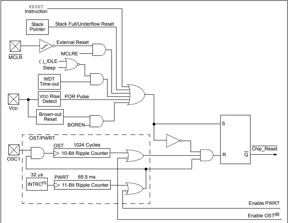
Note 1: This is the low-frequency INTRC source from the internal oscillator block. 2: See Table 4-2 for time-out situations.
REGISTER 4-1: RCON: RESET CONTROL REGISTER
| R/W-0 | R/W-1⁽¹⁾ | U-0 | R/W-1 | R-1 | R-1 | R/W-0⁽²⁾ | R/W-0 |
|---|---|---|---|---|---|---|---|
| IPEN | SBOREN | — | RI | TO | PD | POR | BOR |
| bit 7 | bit 0 |
Legend:
R = Readable bit
W = Writable bit
U = Unimplemented bit, read as ‘0’
-n = Value at POR
‘1’ = Bit is set
‘0’ = Bit is cleared
x = Bit is unknown
bit 7
IPEN: Interrupt Priority Enable bit
1 = Enable priority levels on interrupts
0 = Disable priority levels on interrupts (PIC16CXXX Compatibility mode)
bit 6
SBOREN: BOR Software Enable bit⁽¹⁾
If BOREN1:BOREN0 = 01:
1 = BOR is enabled
0 = BOR is disabled
If BOREN1:BOREN0 = 00, 10 or 11:
Bit is disabled and read as ‘0’.
bit 5
Unimplemented: Read as ‘0’
bit 4
RI: RESET Instruction Flag bit
1 = The RESET instruction was not executed (set by firmware only)
0 = The RESET instruction was executed causing a device Reset (must be set in software after a Brown-out Reset occurs)
bit 3
TO: Watchdog Time-out Flag bit
1 = Set by power-up, CLRWDT instruction or SLEEP instruction
0 = A WDT time-out occurred
bit 2
PD: Power-Down Detection Flag bit
1 = Set by power-up or by the CLRWDT instruction
0 = Set by execution of the SLEEP instruction
bit 1
POR: Power-on Reset Status bit⁽²⁾
1 = A Power-on Reset has not occurred (set by firmware only)
0 = A Power-on Reset occurred (must be set in software after a Power-on Reset occurs)
bit 0
BOR: Brown-out Reset Status bit
1 = A Brown-out Reset has not occurred (set by firmware only)
0 = A Brown-out Reset occurred (must be set in software after a Brown-out Reset occurs)
Note 1: If SBOREN is enabled, its Reset state is ‘1’; otherwise, it is ‘0’.
2: The actual Reset value of POR is determined by the type of device Reset. See the notes following this register and Section 4.6 “Reset State of Registers” for additional information.
Note 1: It is recommended that the POR bit be set after a Power-on Reset has been detected so that subsequent Power-on Resets may be detected.
2: Brown-out Reset is said to have occurred when BOR is ‘0’ and POR is ‘1’ (assuming that POR was set to ‘1’ by software immediately after POR).
4.2 Master Clear Reset (MCLR)
The MCLR pin provides a method for triggering an external Reset of the device. A Reset is generated by holding the pin low. These devices have a noise filter in the MCLR Reset path which detects and ignores small pulses.
The MCLR pin is not driven low by any internal Resets, including the WDT.
In PIC18F2455/2550/4455/4550 devices, the MCLR input can be disabled with the MCLRE Configuration bit. When MCLR is disabled, the pin becomes a digital input. See Section 10.5 “PORTE, TRISE and LATE Registers” for more information.
4.3 Power-on Reset (POR)
A Power-on Reset pulse is generated on-chip whenever VDD rises above a certain threshold. This allows the device to start in the initialized state when VDD is adequate for operation.
To take advantage of the POR circuitry, tie the MCLR pin through a resistor (1 kΩ to 10 kΩ) to VDD. This will eliminate external RC components usually needed to create a Power-on Reset delay. A minimum rise rate for VDD is specified (parameter D004, Section 28.1 “DC Characteristics”). For a slow rise time, see Figure 4-2.
When the device starts normal operation (i.e., exits the Reset condition), device operating parameters (voltage, frequency, temperature, etc.) must be met to ensure operation. If these conditions are not met, the device must be held in Reset until the operating conditions are met.
POR events are captured by the \overlinePOR bit (RCON<1>). The state of the bit is set to ‘0’ whenever a POR occurs; it does not change for any other Reset event. \overlinePOR is not reset to ‘1’ by any hardware event. To capture multiple events, the user manually resets the bit to ‘1’ in software following any POR.
FIGURE 4-2: EXTERNAL POWER-ON RESET CIRCUIT (FOR SLOW VDD POWER-UP)
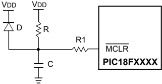
Note 1: External Power-on Reset circuit is required only if the VDD power-up slope is too slow. The diode D helps discharge the capacitor quickly when VDD powers down.
2: R < 40 kΩ is recommended to make sure that the voltage drop across R does not violate the device’s electrical specification.
3: R1 ≥ 1 kΩ will limit any current flowing into MCLR from external capacitor C, in the event of MCLR/VPP pin breakdown, due to Electrostatic Discharge (ESD) or Electrical Overstress (EOS).
4.4 Brown-out Reset (BOR)
PIC18F2455/2550/4455/4550 devices implement a BOR circuit that provides the user with a number of configuration and power-saving options. The BOR is controlled by the BORV1:BORV0 and BOREN1:BOREN0 Configuration bits. There are a total of four BOR configurations which are summarized in Table 4-1.
The BOR threshold is set by the BORV1:BORV0 bits. If BOR is enabled (any values of BOREN1:BOREN0 except ‘00’), any drop of VDD below VBOR (parameter D005, Section 28.1 “DC Characteristics”) for greater than TBOR (parameter 35, Table 28-12) will reset the device. A Reset may or may not occur if VDD falls below VBOR for less than TBOR. The chip will remain in Brown-out Reset until VDD rises above VBOR.
If the Power-up Timer is enabled, it will be invoked after VDD rises above VBOR; it then will keep the chip in Reset for an additional time delay, TPWRT (parameter 33, Table 28-12). If VDD drops below VBOR while the Power-up Timer is running, the chip will go back into a Brown-out Reset and the Power-up Timer will be initialized. Once VDD rises above VBOR, the Power-up Timer will execute the additional time delay.
BOR and the Power-on Timer (PWRT) are independently configured. Enabling BOR Reset does not automatically enable the PWRT.
4.4.1 SOFTWARE ENABLED BOR
When BOREN1:BOREN0 = 01, the BOR can be enabled or disabled by the user in software. This is done with the control bit, SBOREN (RCON<6>). Setting SBOREN enables the BOR to function as previously described. Clearing SBOREN disables the BOR entirely. The SBOREN bit operates only in this mode; otherwise, it is read as ‘0’.
Placing the BOR under software control gives the user the additional flexibility of tailoring the application to its environment without having to reprogram the device to change BOR configuration. It also allows the user to tailor device power consumption in software by eliminating the incremental current that the BOR consumes. While the BOR current is typically very small, it may have some impact in low-power applications.
Note: Even when BOR is under software control, the BOR Reset voltage level is still set by the BORV1:BORV0 Configuration bits. It cannot be changed in software.
4.4.2 DETECTING BOR
When BOR is enabled, the BOR bit always resets to ‘0’ on any BOR or POR event. This makes it difficult to determine if a BOR event has occurred just by reading the state of BOR alone. A more reliable method is to simultaneously check the state of both POR and BOR. This assumes that the POR bit is reset to ‘1’ in software immediately after any POR event. IF BOR is ‘0’ while POR is ‘1’, it can be reliably assumed that a BOR event has occurred.
4.4.3 DISABLING BOR IN SLEEP MODE
When BOREN1:BOREN0 = 10, the BOR remains under hardware control and operates as previously described. Whenever the device enters Sleep mode, however, the BOR is automatically disabled. When the device returns to any other operating mode, BOR is automatically re-enabled.
This mode allows for applications to recover from brown-out situations, while actively executing code, when the device requires BOR protection the most. At the same time, it saves additional power in Sleep mode by eliminating the small incremental BOR current.
TABLE 4-1: BOR CONFIGURATIONS
| BOR Configuration | Status of SBOREN (RCON<6>) | BOR Operation | |
|---|---|---|---|
| BOREN1 | BOREN0 | ||
| 0 | 0 | Unavailable | BOR disabled; must be enabled by reprogramming the Configuration bits. |
| 0 | 1 | Available | BOR enabled in software; operation controlled by SBOREN. |
| 1 | 0 | Unavailable | BOR enabled in hardware in Run and Idle modes, disabled during Sleep mode. |
| 1 | 1 | Unavailable | BOR enabled in hardware; must be disabled by reprogramming the Configuration bits. |
4.5 Device Reset Timers
PIC18F2455/2550/4455/4550 devices incorporate three separate on-chip timers that help regulate the Power-on Reset process. Their main function is to ensure that the device clock is stable before code is executed. These timers are:
- Power-up Timer (PWRT)
- Oscillator Start-up Timer (OST)
- PLL Lock Time-out
4.5.1 POWER-UP TIMER (PWRT)
The Power-up Timer (PWRT) of the PIC18F2455/2550/4455/4550 devices is an 11-bit counter which uses the INTRC source as the clock input. This yields an approximate time interval of 2048 x 32 µs = 65.6 ms. While the PWRT is counting, the device is held in Reset.
The power-up time delay depends on the INTRC clock and will vary from chip to chip due to temperature and process variation. See DC parameter 33 (Table 28-12) for details.
The PWRT is enabled by clearing the PWRTEN Configuration bit.
4.5.2 OSCILLATOR START-UP TIMER (OST)
The Oscillator Start-up Timer (OST) provides a 1024 oscillator cycle (from OSC1 input) delay after the PWRT delay is over (parameter 33, Table 28-12). This ensures that the crystal oscillator or resonator has started and stabilized.
The OST time-out is invoked only for XT, HS and HSPLL modes and only on Power-on Reset or on exit from most power-managed modes.
4.5.3 PLL LOCK TIME-OUT
With the PLL enabled in its PLL mode, the time-out sequence following a Power-on Reset is slightly different from other oscillator modes. A separate timer is used to provide a fixed time-out that is sufficient for the PLL to lock to the main oscillator frequency. This PLL lock time-out (TPLL) is typically 2 ms and follows the oscillator start-up time-out.
4.5.4 TIME-OUT SEQUENCE
On power-up, the time-out sequence is as follows:
- After the POR condition has cleared, PWRT time-out is invoked (if enabled).
- Then, the OST is activated.
The total time-out will vary based on oscillator configuration and the status of the PWRT. Figure 4-3, Figure 4-4, Figure 4-5, Figure 4-6 and Figure 4-7 all depict time-out sequences on power-up, with the Power-up Timer enabled and the device operating in HS Oscillator mode. Figures 4-3 through 4-6 also apply to devices operating in XT mode. For devices in RC mode and with the PWRT disabled, on the other hand, there will be no time-out at all.
Since the time-outs occur from the POR pulse, if MCLR is kept low long enough, all time-outs will expire. Bringing MCLR high will begin execution immediately (Figure 4-5). This is useful for testing purposes or to synchronize more than one PIC18FXXXX device operating in parallel.
TABLE 4-2: TIME-OUT IN VARIOUS SITUATIONS
| Oscillator Configuration | Power-up(2) and Brown-out | Exit from Power-Managed Mode | |
|---|---|---|---|
| PWRTEN = 0 | PWRTEN = 1 | ||
| HS, XT | 66 ms(1) + 1024 Tosc | 1024 Tosc | 1024 Tosc |
| HSPLL, XTPLL | 66 ms(1) + 1024 Tosc + 2 ms(2) | 1024 Tosc + 2 ms(2) | 1024 Tosc + 2 ms(2) |
| EC, ECIO | 66 ms(1) | — | — |
| ECPLL, ECPIO | 66 ms(1) + 2 ms(2) | 2 ms(2) | 2 ms(2) |
| INTIO, INTCKO | 66 ms(1) | — | — |
| INTHS, INTXT | 66 ms(1) + 1024 Tosc | 1024 Tosc | 1024 Tosc |
Note 1: 66 ms (65.5 ms) is the nominal Power-up Timer (PWRT) delay.
2: 2 ms is the nominal time required for the PLL to lock.
FIGURE 4-3: TIME-OUT SEQUENCE ON POWER-UP (\overlineMCLR TIED TO VDD, VDD RISE < TPWRT)
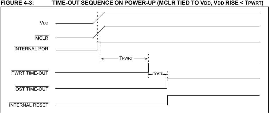
FIGURE 4-4: TIME-OUT SEQUENCE ON POWER-UP (\overlineMCLR NOT TIED TO VDD): CASE 1
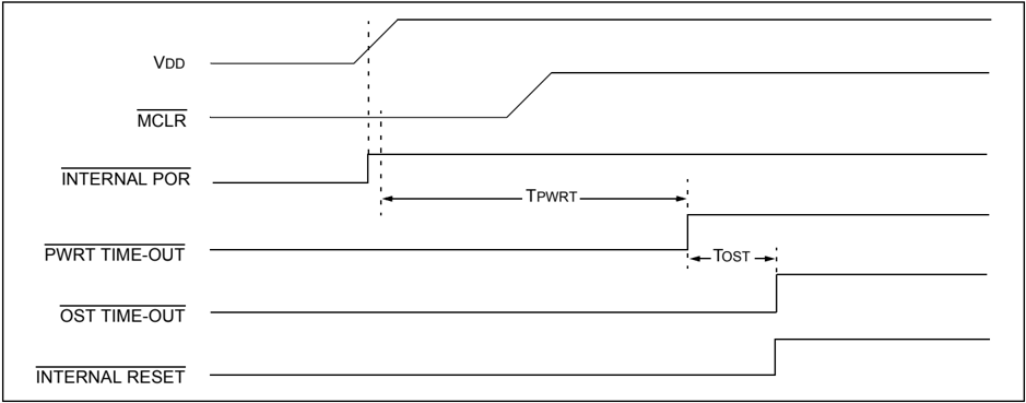
FIGURE 4-5: TIME-OUT SEQUENCE ON POWER-UP (\overlineMCLR NOT TIED TO VDD): CASE 2
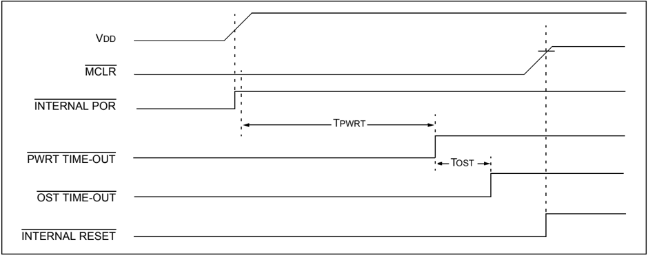
FIGURE 4-6: SLOW RISE TIME (\overlineMCLR TIED TO VDD, VDD RISE > TPWRT)
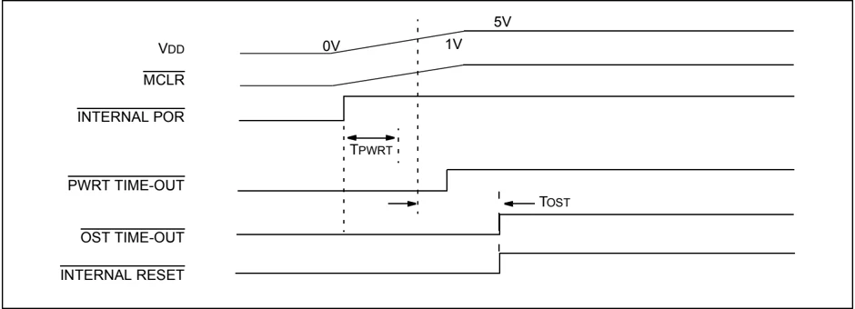
FIGURE 4-7: TIME-OUT SEQUENCE ON POR w/PLL ENABLED (\overlineMCLR TIED TO VDD)
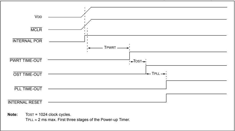
Note: TOST = 1024 clock cycles. TPLL ≈ 2 ms max. First three stages of the Power-up Timer.
4.6 Reset State of Registers
Most registers are unaffected by a Reset. Their status is unknown on POR and unchanged by all other Resets. The other registers are forced to a “Reset state” depending on the type of Reset that occurred.
Most registers are not affected by a WDT wake-up, since this is viewed as the resumption of normal operation. Status bits from the RCON register, RI, TO, PD, POR and BOR, are set or cleared differently in different Reset situations as indicated in Table 4-3. These bits are used in software to determine the nature of the Reset.
Table 4-4 describes the Reset states for all of the Special Function Registers. These are categorized by Power-on and Brown-out Resets, Master Clear and WDT Resets and WDT wake-ups.
TABLE 4-3: STATUS BITS, THEIR SIGNIFICANCE AND THE INITIALIZATION CONDITION FOR RCON REGISTER
| Condition | Program Counter | RCON Register | STKPTR Register | |||||
|---|---|---|---|---|---|---|---|---|
| RI | TO | PD | POR | BOR | STKFUL | STKUNF | ||
| Power-on Reset | 0000h | 1 | 1 | 1 | 0 | 0 | 0 | 0 |
| RESET instruction | 0000h | 0 | u | u | u | u | u | u |
| Brown-out Reset | 0000h | 1 | 1 | 1 | u | 0 | u | u |
| MCLR Reset during power-managed Run modes | 0000h | u | 1 | u | u | u | u | u |
| MCLR Reset during power-managed Idle modes and Sleep mode | 0000h | u | 1 | 0 | u | u | u | u |
| WDT time-out during full power or power-managed Run modes | 0000h | u | 0 | u | u | u | u | u |
| MCLR Reset during full-power execution | 0000h | u | u | u | u | u | u | u |
| Stack Full Reset (STVREN = 1) | 0000h | u | u | u | u | u | 1 | u |
| Stack Underflow Reset (STVREN = 1) | 0000h | u | u | u | u | u | u | 1 |
| Stack Underflow Error (not an actual Reset, STVREN = 0) | 0000h | u | u | u | u | u | u | 1 |
| WDT time-out during power-managed Idle or Sleep modes | PC + 2 | u | 0 | 0 | u | u | u | u |
| Interrupt exit from power-managed modes | PC + 2(1) | u | u | 0 | u | u | u | u |
Legend: u = unchanged
Note 1: When the wake-up is due to an interrupt and the GIEH or GIEL bits are set, the PC is loaded with the interrupt vector (008h or 0018h).
2: Reset state is ‘1’ for POR and unchanged for all other Resets when software BOR is enabled (BOREN1:BOREN0 Configuration bits = 01 and SBOREN = 1); otherwise, the Reset state is ‘0’.
TABLE 4-4: INITIALIZATION CONDITIONS FOR ALL REGISTERS
| Register | Applicable Devices | Power-on Reset, Brown-out Reset | MCLR Resets, WDT Reset, RESET Instruction, Stack Resets | Wake-up via WDT or Interrupt |
|---|---|---|---|---|
| TOSU | 2455 2550 4455 4550 | ---0 0000 | ---0 0000 | ---0 uuuu(1) |
| TOSH | 2455 2550 4455 4550 | 0000 0000 | 0000 0000 | uuuu uuuu(1) |
| TOSL | 2455 2550 4455 4550 | 0000 0000 | 0000 0000 | uuuu uuuu(1) |
| STKPTR | 2455 2550 4455 4550 | 00-0 0000 | uu-0 0000 | uu-u uuuu(1) |
| PCLATU | 2455 2550 4455 4550 | ---0 0000 | ---0 0000 | ---u uuuu |
| PCLATH | 2455 2550 4455 4550 | 0000 0000 | 0000 0000 | uuuu uuuu |
| PCL | 2455 2550 4455 4550 | 0000 0000 | 0000 0000 | PC + 2(3) |
| TBLPTRU | 2455 2550 4455 4550 | --00 0000 | --00 0000 | --uu uuuu |
| TBLPTRH | 2455 2550 4455 4550 | 0000 0000 | 0000 0000 | uuuu uuuu |
| TBLPTRL | 2455 2550 4455 4550 | 0000 0000 | 0000 0000 | uuuu uuuu |
| TABLAT | 2455 2550 4455 4550 | 0000 0000 | 0000 0000 | uuuu uuuu |
| PRODH | 2455 2550 4455 4550 | xxxx xxxx | uuuu uuuu | uuuu uuuu |
| PRODL | 2455 2550 4455 4550 | xxxx xxxx | uuuu uuuu | uuuu uuuu |
| INTCON | 2455 2550 4455 4550 | 0000 000x | 0000 000u | uuuu uuuu(2) |
| INTCON2 | 2455 2550 4455 4550 | 1111 -1-1 | 1111 -1-1 | uuuu -u-u(2) |
| INTCON3 | 2455 2550 4455 4550 | 11-0 0-00 | 11-0 0-00 | uu-u u-uu(2) |
| INDF0 | 2455 2550 4455 4550 | N/A | N/A | N/A |
| POSTINC0 | 2455 2550 4455 4550 | N/A | N/A | N/A |
| POSTDEC0 | 2455 2550 4455 4550 | N/A | N/A | N/A |
| PREINC0 | 2455 2550 4455 4550 | N/A | N/A | N/A |
| PLUSW0 | 2455 2550 4455 4550 | N/A | N/A | N/A |
| FSR0H | 2455 2550 4455 4550 | ---- 0000 | ---- 0000 | ---- uuuu |
| FSR0L | 2455 2550 4455 4550 | xxxx xxxx | uuuu uuuu | uuuu uuuu |
| WREG | 2455 2550 4455 4550 | xxxx xxxx | uuuu uuuu | uuuu uuuu |
| INDF1 | 2455 2550 4455 4550 | N/A | N/A | N/A |
| POSTINC1 | 2455 2550 4455 4550 | N/A | N/A | N/A |
| POSTDEC1 | 2455 2550 4455 4550 | N/A | N/A | N/A |
| PREINC1 | 2455 2550 4455 4550 | N/A | N/A | N/A |
| PLUSW1 | 2455 2550 4455 4550 | N/A | N/A | N/A |
| FSR1H | 2455 2550 4455 4550 | ---- 0000 | ---- 0000 | ---- uuuu |
| FSR1L | 2455 2550 4455 4550 | xxxx xxxx | uuuu uuuu | uuuu uuuu |
| BSR | 2455 2550 4455 4550 | ---- 0000 | ---- 0000 | ---- uuuu |
Legend: u = unchanged, x = unknown, - = unimplemented bit, read as ‘0’, q = value depends on condition.
Shaded cells indicate conditions do not apply for the designated device.
Note 1: When the wake-up is due to an interrupt and the GIEL or GIEH bit is set, the TOSU, TOSH and TOSL are updated with the current value of the PC. The STKPTR is modified to point to the next location in the hardware stack.
2: One or more bits in the INTCONx or PIRx registers will be affected (to cause wake-up).
3: When the wake-up is due to an interrupt and the GIEL or GIEH bit is set, the PC is loaded with the interrupt vector (0008h or 0018h).
4: See Table 4-3 for Reset value for specific condition.
5: PORTA<6>, LATA<6> and TRISA<6> are enabled depending on the oscillator mode selected. When not enabled as PORTA pins, they are disabled and read ‘0’.
TABLE 4-4: INITIALIZATION CONDITIONS FOR ALL REGISTERS (CONTINUED)
| Register | Applicable Devices | Power-on Reset, Brown-out Reset | MCLR Resets, WDT Reset, RESET Instruction, Stack Resets | Wake-up via WDT or Interrupt |
|---|---|---|---|---|
| IND2F | 2455 2550 4455 4550 | N/A | N/A | N/A |
| POSTINC2 | 2455 2550 4455 4550 | N/A | N/A | N/A |
| POSTDEC2 | 2455 2550 4455 4550 | N/A | N/A | N/A |
| PREINC2 | 2455 2550 4455 4550 | N/A | N/A | N/A |
| PLUSW2 | 2455 2550 4455 4550 | N/A | N/A | N/A |
| FSR2H | 2455 2550 4455 4550 | ---- 0000 | ---- 0000 | ---- uuuu |
| FSR2L | 2455 2550 4455 4550 | xxxx xxxx | uuuu uuuu | uuuu uuuu |
| STATUS | 2455 2550 4455 4550 | ---x xxxx | ---u uuuu | ---u uuuu |
| TMR0H | 2455 2550 4455 4550 | 0000 0000 | 0000 0000 | uuuu uuuu |
| TMR0L | 2455 2550 4455 4550 | xxxx xxxx | uuuu uuuu | uuuu uuuu |
| T0CON | 2455 2550 4455 4550 | 1111 1111 | 1111 1111 | uuuu uuuu |
| OSCCON | 2455 2550 4455 4550 | 0100 q000 | 0100 00q0 | uuuu uuqu |
| HLVDCON | 2455 2550 4455 4550 | 0-00 0101 | 0-00 0101 | u-uu uuuu |
| WDTCON | 2455 2550 4455 4550 | ---- ---0 | ---- ---0 | ---- ---u |
| RCON(4) | 2455 2550 4455 4550 | 0q-1 11q0 | 0q-q qquu | uq-u qquu |
| TMR1H | 2455 2550 4455 4550 | xxxx xxxx | uuuu uuuu | uuuu uuuu |
| TMR1L | 2455 2550 4455 4550 | xxxx xxxx | uuuu uuuu | uuuu uuuu |
| T1CON | 2455 2550 4455 4550 | 0000 0000 | u0uu uuuu | uuuu uuuu |
| TMR2 | 2455 2550 4455 4550 | 0000 0000 | 0000 0000 | uuuu uuuu |
| PR2 | 2455 2550 4455 4550 | 1111 1111 | 1111 1111 | 1111 1111 |
| T2CON | 2455 2550 4455 4550 | -000 0000 | -000 0000 | -uuu uuuu |
| SSPBUF | 2455 2550 4455 4550 | xxxx xxxx | uuuu uuuu | uuuu uuuu |
| SSPADD | 2455 2550 4455 4550 | 0000 0000 | 0000 0000 | uuuu uuuu |
| SSPSTAT | 2455 2550 4455 4550 | 0000 0000 | 0000 0000 | uuuu uuuu |
| SSPCON1 | 2455 2550 4455 4550 | 0000 0000 | 0000 0000 | uuuu uuuu |
| SSPCON2 | 2455 2550 4455 4550 | 0000 0000 | 0000 0000 | uuuu uuuu |
| ADRESH | 2455 2550 4455 4550 | xxxx xxxx | uuuu uuuu | uuuu uuuu |
| ADRESL | 2455 2550 4455 4550 | xxxx xxxx | uuuu uuuu | uuuu uuuu |
| ADCON0 | 2455 2550 4455 4550 | --00 0000 | --00 0000 | --uu uuuu |
| ADCON1 | 2455 2550 4455 4550 | --00 0qqq | --00 0qqq | --uu uuuu |
| ADCON2 | 2455 2550 4455 4550 | 0-00 0000 | 0-00 0000 | u-uu uuuu |
Legend: u = unchanged, x = unknown, - = unimplemented bit, read as ‘0’, q = value depends on condition.
Shaded cells indicate conditions do not apply for the designated device.
Note 1: When the wake-up is due to an interrupt and the GIEL or GIEH bit is set, the TOSU, TOSH and TOSL are updated with the current value of the PC. The STKPTR is modified to point to the next location in the hardware stack.
2: One or more bits in the INTCONx or PIRx registers will be affected (to cause wake-up).
3: When the wake-up is due to an interrupt and the GIEL or GIEH bit is set, the PC is loaded with the interrupt vector (0008h or 0018h).
4: See Table 4-3 for Reset value for specific condition.
5: PORTA<6>, LATA<6> and TRISA<6> are enabled depending on the oscillator mode selected. When not enabled as PORTA pins, they are disabled and read ‘0’.
DS39632E-page 54 © 2009 Microchip Technology Inc.
TABLE 4-4: INITIALIZATION CONDITIONS FOR ALL REGISTERS (CONTINUED)
| Register | Applicable Devices | Power-on Reset, Brown-out Reset | MCLR Resets, WDT Reset, RESET Instruction, Stack Resets | Wake-up via WDT or Interrupt |
|---|---|---|---|---|
| CCPR1H | 2455 2550 4455 4550 | xxxx xxxx | uuuu uuuu | uuuu uuuu |
| CCPR1L | 2455 2550 4455 4550 | xxxx xxxx | uuuu uuuu | uuuu uuuu |
| CCP1CON | 2455 2550 4455 4550 | --00 0000 | --00 0000 | --uu uuuu |
| 2455 2550 4455 4550 | 0000 0000 | 0000 0000 | uuuu uuuu | |
| CCPR2H | 2455 2550 4455 4550 | xxxx xxxx | uuuu uuuu | uuuu uuuu |
| CCPR2L | 2455 2550 4455 4550 | xxxx xxxx | uuuu uuuu | uuuu uuuu |
| CCP2CON | 2455 2550 4455 4550 | --00 0000 | --00 0000 | --uu uuuu |
| BAUDCON | 2455 2550 4455 4550 | 0100 0-00 | 0100 0-00 | uuuu u-uu |
| ECCP1DEL | 2455 2550 4455 4550 | 0000 0000 | 0000 0000 | uuuu uuuu |
| ECCP1AS | 2455 2550 4455 4550 | 0000 0000 | 0000 0000 | uuuu uuuu |
| CVRCON | 2455 2550 4455 4550 | 0000 0000 | 0000 0000 | uuuu uuuu |
| CMCON | 2455 2550 4455 4550 | 0000 0111 | 0000 0111 | uuuu uuuu |
| TMR3H | 2455 2550 4455 4550 | xxxx xxxx | uuuu uuuu | uuuu uuuu |
| TMR3L | 2455 2550 4455 4550 | xxxx xxxx | uuuu uuuu | uuuu uuuu |
| T3CON | 2455 2550 4455 4550 | 0000 0000 | uuuu uuuu | uuuu uuuu |
| SPBRGH | 2455 2550 4455 4550 | 0000 0000 | 0000 0000 | uuuu uuuu |
| SPBRG | 2455 2550 4455 4550 | 0000 0000 | 0000 0000 | uuuu uuuu |
| RCREG | 2455 2550 4455 4550 | 0000 0000 | 0000 0000 | uuuu uuuu |
| TXREG | 2455 2550 4455 4550 | 0000 0000 | 0000 0000 | uuuu uuuu |
| TXSTA | 2455 2550 4455 4550 | 0000 0010 | 0000 0010 | uuuu uuuu |
| RCSTA | 2455 2550 4455 4550 | 0000 000x | 0000 000x | uuuu uuuu |
| EEADR | 2455 2550 4455 4550 | 0000 0000 | 0000 0000 | uuuu uuuu |
| EEDATA | 2455 2550 4455 4550 | 0000 0000 | 0000 0000 | uuuu uuuu |
| EECON2 | 2455 2550 4455 4550 | 0000 0000 | 0000 0000 | 0000 0000 |
| EECON1 | 2455 2550 4455 4550 | xx-0 x000 | uu-0 u000 | uu-0 u000 |
Legend: u = unchanged, x = unknown, - = unimplemented bit, read as ‘0’, q = value depends on condition.
Shaded cells indicate conditions do not apply for the designated device.
Note 1: When the wake-up is due to an interrupt and the GIEL or GIEH bit is set, the TOSU, TOSH and TOSL are updated with the current value of the PC. The STKPTR is modified to point to the next location in the hardware stack.
2: One or more bits in the INTCONx or PIRx registers will be affected (to cause wake-up).
3: When the wake-up is due to an interrupt and the GIEL or GIEH bit is set, the PC is loaded with the interrupt vector (0008h or 0018h).
4: See Table 4-3 for Reset value for specific condition.
5: PORTA<6>, LATA<6> and TRISA<6> are enabled depending on the oscillator mode selected. When not enabled as PORTA pins, they are disabled and read ‘0’.
TABLE 4-4: INITIALIZATION CONDITIONS FOR ALL REGISTERS (CONTINUED)
| Register | Applicable Devices | Power-on Reset, Brown-out Reset | MCLR Resets, WDT Reset, RESET Instruction, Stack Resets | Wake-up via WDT or Interrupt |
|---|---|---|---|---|
| IPR2 | 2455 2550 4455 4550 | 1111 1111 | 1111 1111 | uuuu uuuu |
| PIR2 | 2455 2550 4455 4550 | 0000 0000 | 0000 0000 | uuuu uuuu(2) |
| PIE2 | 2455 2550 4455 4550 | 0000 0000 | 0000 0000 | uuuu uuuu |
| IPR1 | 2455 2550 4455 4550 | 1111 1111 | 1111 1111 | uuuu uuuu |
| 2455 2550 4455 4550 | -111 1111 | -111 1111 | -uuu uuuu | |
| PIR1 | 2455 2550 4455 4550 | 0000 0000 | 0000 0000 | uuuu uuuu(2) |
| 2455 2550 4455 4550 | -000 0000 | -000 0000 | -uuu uuuu | |
| PIE1 | 2455 2550 4455 4550 | 0000 0000 | 0000 0000 | uuuu uuuu |
| 2455 2550 4455 4550 | -000 0000 | -000 0000 | -uuu uuuu | |
| OSCTUNE | 2455 2550 4455 4550 | 0--0 0000 | 0--0 0000 | u--u uuuu |
| TRISE | 2455 2550 4455 4550 | ---- -111 | ---- -111 | ---- -uuu |
| TRISD | 2455 2550 4455 4550 | 1111 1111 | 1111 1111 | uuuu uuuu |
| TRISC | 2455 2550 4455 4550 | 11-- -111 | 11-- -111 | uu-- -uuu |
| TRISB | 2455 2550 4455 4550 | 1111 1111 | 1111 1111 | uuuu uuuu |
| TRISA(5) | 2455 2550 4455 4550 | -111 1111(5) | -111 1111(5) | -uuu uuuu(5) |
| LATE | 2455 2550 4455 4550 | ---- -xxx | ---- -uuu | ---- -uuu |
| LATD | 2455 2550 4455 4550 | xxxx xxxx | uuuu uuuu | uuuu uuuu |
| LATC | 2455 2550 4455 4550 | xx-- -xxx | uu-- -uuu | uu-- -uuu |
| LATB | 2455 2550 4455 4550 | xxxx xxxx | uuuu uuuu | uuuu uuuu |
| LATA(5) | 2455 2550 4455 4550 | -xxx xxxx(5) | -uuu uuuu(5) | -uuu uuuu(5) |
| PORTE | 2455 2550 4455 4550 | 0--- x000 | 0--- x000 | u--- uuuu |
| PORTD | 2455 2550 4455 4550 | xxxx xxxx | uuuu uuuu | uuuu uuuu |
| PORTC | 2455 2550 4455 4550 | xxxx -xxx | uuuu -uuu | uuuu -uuu |
| PORTB | 2455 2550 4455 4550 | xxxx xxxx | uuuu uuuu | uuuu uuuu |
| PORTA(5) | 2455 2550 4455 4550 | -x0x 0000(5) | -u0u 0000(5) | -uuu uuuu(5) |
Legend: u = unchanged, x = unknown, - = unimplemented bit, read as ‘0’, q = value depends on condition.
Shaded cells indicate conditions do not apply for the designated device.
Note 1: When the wake-up is due to an interrupt and the GIEL or GIEH bit is set, the TOSU, TOSH and TOSL are updated with the current value of the PC. The STKPTR is modified to point to the next location in the hardware stack.
2: One or more bits in the INTCONx or PIRx registers will be affected (to cause wake-up).
3: When the wake-up is due to an interrupt and the GIEL or GIEH bit is set, the PC is loaded with the interrupt vector (0008h or 0018h).
4: See Table 4-3 for Reset value for specific condition.
5: PORTA<6>, LATA<6> and TRISA<6> are enabled depending on the oscillator mode selected. When not enabled as PORTA pins, they are disabled and read ‘0’.
DS39632E-page 56 © 2009 Microchip Technology Inc.
TABLE 4-4: INITIALIZATION CONDITIONS FOR ALL REGISTERS (CONTINUED)
| Register | Applicable Devices | Power-on Reset, Brown-out Reset | MCLR Resets, WDT Reset, RESET Instruction, Stack Resets | Wake-up via WDT or Interrupt |
|---|---|---|---|---|
| UEP15 | 2455 2550 4455 4550 | ---0 0000 | ---0 0000 | ---u uuuu |
| UEP14 | 2455 2550 4455 4550 | ---0 0000 | ---0 0000 | ---u uuuu |
| UEP13 | 2455 2550 4455 4550 | ---0 0000 | ---0 0000 | ---u uuuu |
| UEP12 | 2455 2550 4455 4550 | ---0 0000 | ---0 0000 | ---u uuuu |
| UEP11 | 2455 2550 4455 4550 | ---0 0000 | ---0 0000 | ---u uuuu |
| UEP10 | 2455 2550 4455 4550 | ---0 0000 | ---0 0000 | ---u uuuu |
| UEP9 | 2455 2550 4455 4550 | ---0 0000 | ---0 0000 | ---u uuuu |
| UEP8 | 2455 2550 4455 4550 | ---0 0000 | ---0 0000 | ---u uuuu |
| UEP7 | 2455 2550 4455 4550 | ---0 0000 | ---0 0000 | ---u uuuu |
| UEP6 | 2455 2550 4455 4550 | ---0 0000 | ---0 0000 | ---u uuuu |
| UEP5 | 2455 2550 4455 4550 | ---0 0000 | ---0 0000 | ---u uuuu |
| UEP4 | 2455 2550 4455 4550 | ---0 0000 | ---0 0000 | ---u uuuu |
| UEP3 | 2455 2550 4455 4550 | ---0 0000 | ---0 0000 | ---u uuuu |
| UEP2 | 2455 2550 4455 4550 | ---0 0000 | ---0 0000 | ---u uuuu |
| UEP1 | 2455 2550 4455 4550 | ---0 0000 | ---0 0000 | ---u uuuu |
| UEP0 | 2455 2550 4455 4550 | ---0 0000 | ---0 0000 | ---u uuuu |
| UCFG | 2455 2550 4455 4550 | 00-0 0000 | 00-0 0000 | uu-u uuuu |
| UADDR | 2455 2550 4455 4550 | -000 0000 | -000 0000 | -uuu uuuu |
| UCON | 2455 2550 4455 4550 | -0x0 000- | -0x0 000- | -uuu uuu- |
| USTAT | 2455 2550 4455 4550 | -xxx xxx- | -xxx xxx- | -uuu uuu- |
| UEIE | 2455 2550 4455 4550 | 0--0 0000 | 0--0 0000 | u--u uuuu |
| UEIR | 2455 2550 4455 4550 | 0--0 0000 | 0--0 0000 | u--u uuuu |
| UIE | 2455 2550 4455 4550 | -000 0000 | -000 0000 | -uuu uuuu |
| UIR | 2455 2550 4455 4550 | -000 0000 | -000 0000 | -uuu uuuu |
| UFRMH | 2455 2550 4455 4550 | ---- -xxx | ---- -xxx | ---- -uuu |
| UFRML | 2455 2550 4455 4550 | xxxx xxxx | xxxx xxxx | uuuu uuuu |
| SPPCON | 2455 2550 4455 4550 | ---- --00 | ---- --00 | ---- --uu |
| SPPEPS | 2455 2550 4455 4550 | 00-0 0000 | 00-0 0000 | uu-u uuuu |
| SPPCFG | 2455 2550 4455 4550 | 0000 0000 | 0000 0000 | uuuu uuuu |
| SPPDATA | 2455 2550 4455 4550 | 0000 0000 | 0000 0000 | uuuu uuuu |
Legend: u = unchanged, x = unknown, - = unimplemented bit, read as ‘0’, q = value depends on condition.
Shaded cells indicate conditions do not apply for the designated device.
Note 1: When the wake-up is due to an interrupt and the GIEL or GIEH bit is set, the TOSU, TOSH and TOSL are updated with the current value of the PC. The STKPTR is modified to point to the next location in the hardware stack.
2: One or more bits in the INTCONx or PIRx registers will be affected (to cause wake-up).
3: When the wake-up is due to an interrupt and the GIEL or GIEH bit is set, the PC is loaded with the interrupt vector (0008h or 0018h).
4: See Table 4-3 for Reset value for specific condition.
5: PORTA<6>, LATA<6> and TRISA<6> are enabled depending on the oscillator mode selected. When not enabled as PORTA pins, they are disabled and read ‘0’.
NOTES:
DS39632E-page 58 © 2009 Microchip Technology Inc.
5.0 MEMORY ORGANIZATION
There are three types of memory in PIC18 enhanced microcontroller devices:
- Program Memory
- Data RAM
- Data EEPROM
As Harvard architecture devices, the data and program memories use separate busses; this allows for concurrent access of the two memory spaces. The data EEPROM, for practical purposes, can be regarded as a peripheral device, since it is addressed and accessed through a set of control registers.
Additional detailed information on the operation of the Flash program memory is provided in Section 6.0 “Flash Program Memory”. Data EEPROM is discussed separately in Section 7.0 “Data EEPROM Memory”.
5.1 Program Memory Organization
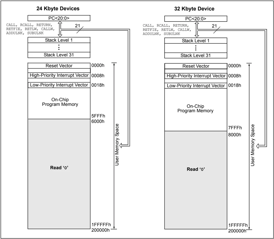
PIC18 microcontrollers implement a 21-bit program counter which is capable of addressing a 2-Mbyte program memory space. Accessing a location between the upper boundary of the physically implemented memory and the 2-Mbyte address will return all ‘0’s (a NOP instruction).
The PIC18F2455 and PIC18F4455 each have 24 Kbytes of Flash memory and can store up to 12,288 single-word instructions. The PIC18F2550 and PIC18F4550 each have 32 Kbytes of Flash memory and can store up to 16,384 single-word instructions.
PIC18 devices have two interrupt vectors. The Reset vector address is at 0000h and the interrupt vector addresses are at 0008h and 0018h.
The program memory maps for PIC18FX455 and PIC18FX550 devices are shown in Figure 5-1.
FIGURE 5-1: PROGRAM MEMORY MAP AND STACK
5.1.1 PROGRAM COUNTER
The Program Counter (PC) specifies the address of the instruction to fetch for execution. The PC is 21 bits wide and is contained in three separate 8-bit registers. The low byte, known as the PCL register, is both readable and writable. The high byte, or PCH register, contains the PC<15:8> bits; it is not directly readable or writable. Updates to the PCH register are performed through the PCLATH register. The upper byte is called PCU. This register contains the PC<20:16> bits; it is also not directly readable or writable. Updates to the PCU register are performed through the PCLATU register.
The contents of PCLATH and PCLATU are transferred to the program counter by any operation that writes PCL. Similarly, the upper two bytes of the program counter are transferred to PCLATH and PCLATU by an operation that reads PCL. This is useful for computed offsets to the PC (see Section 5.1.4.1 "Computed GOTO").
The PC addresses bytes in the program memory. To prevent the PC from becoming misaligned with word instructions, the Least Significant bit of PCL is fixed to a value of '0'. The PC increments by 2 to address sequential instructions in the program memory.
The CALL, RCALL and GOTO program branch instructions write to the program counter directly. For these instructions, the contents of PCLATH and PCLATU are not transferred to the program counter.
5.1.2 RETURN ADDRESS STACK
The return address stack allows any combination of up to 31 program calls and interrupts to occur. The PC is pushed onto the stack when a CALL or RCALL instruction is executed or an interrupt is Acknowledged. The PC value is pulled off the stack on a RETURN, RETLW or a RETFIE instruction. PCLATU and PCLATH are not affected by any of the RETURN or CALL instructions.
The stack operates as a 31-word by 21-bit RAM and a 5-bit Stack Pointer, STKPTR. The stack space is not part of either program or data space. The Stack Pointer is readable and writable and the address on the top of the stack is readable and writable through the Top-of-Stack Special Function Registers. Data can also be pushed to, or popped from the stack, using these registers.
A CALL type instruction causes a push onto the stack. The Stack Pointer is first incremented and the location pointed to by the Stack Pointer is written with the contents of the PC (already pointing to the instruction following the CALL). A RETURN type instruction causes a pop from the stack. The contents of the location pointed to by the STKPTR are transferred to the PC and then the Stack Pointer is decremented.
The Stack Pointer is initialized to '00000' after all Resets. There is no RAM associated with the location corresponding to a Stack Pointer value of '00000'; this is only a Reset value. Status bits indicate if the stack is full, has overflowed or has underflowed.
5.1.2.1 Top-of-Stack Access
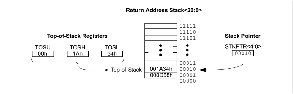
Only the top of the return address stack (TOS) is readable and writable. A set of three registers, TOSU:TOSH:TOSL, hold the contents of the stack location pointed to by the STKPTR register (Figure 5-2). This allows users to implement a software stack if necessary. After a CALL, RCALL or interrupt, the software can read the pushed value by reading the TOSU:TOSH:TOSL registers. These values can be placed on a user-defined software stack. At return time, the software can return these values to TOSU:TOSH:TOSL and do a return.
The user must disable the global interrupt enable bits while accessing the stack to prevent inadvertent stack corruption.
FIGURE 5-2: RETURN ADDRESS STACK AND ASSOCIATED REGISTERS
5.1.2.2 Return Stack Pointer (STKPTR)
The STKPTR register (Register 5-1) contains the Stack Pointer value, the STKFUL (Stack Full) status bit and the STKUNF (Stack Underflow) status bit. The value of the Stack Pointer can be 0 through 31. The Stack Pointer increments before values are pushed onto the stack and decrements after values are popped off the stack. On Reset, the Stack Pointer value will be zero. The user may read and write the Stack Pointer value. This feature can be used by a Real-Time Operating System (RTOS) for return stack maintenance.
After the PC is pushed onto the stack 31 times (without popping any values off the stack), the STKFUL bit is set. The STKFUL bit is cleared by software or by a POR.
The action that takes place when the stack becomes full depends on the state of the STVREN (Stack Overflow Reset Enable) Configuration bit. (Refer to Section 25.1 "Configuration Bits" for a description of the device Configuration bits.) If STVREN is set (default), the 31st push will push the (PC + 2) value onto the stack, set the STKFUL bit and reset the device. The STKFUL bit will remain set and the Stack Pointer will be set to zero.
If STVREN is cleared, the STKFUL bit will be set on the 31st push and the Stack Pointer will increment to 31. Any additional pushes will not overwrite the 31st push and the STKPTR will remain at 31.
When the stack has been popped enough times to unload the stack, the next pop will return a value of zero to the PC and sets the STKUNF bit, while the Stack Pointer remains at zero. The STKUNF bit will remain set until cleared by software or until a POR occurs.
Note: Returning a value of zero to the PC on an underflow has the effect of vectoring the program to the Reset vector, where the stack conditions can be verified and appropriate actions can be taken. This is not the same as a Reset, as the contents of the SFRs are not affected.
5.1.2.3 PUSH and POP Instructions
Since the Top-of-Stack is readable and writable, the ability to push values onto the stack and pull values off the stack, without disturbing normal program execution, is a desirable feature. The PIC18 instruction set includes two instructions, PUSH and POP, that permit the TOS to be manipulated under software control. TOSU, TOSH and TOSL can be modified to place data or a return address on the stack.
The PUSH instruction places the current PC value onto the stack. This increments the Stack Pointer and loads the current PC value onto the stack.
The POP instruction discards the current TOS by decrementing the Stack Pointer. The previous value pushed onto the stack then becomes the TOS value.
REGISTER 5-1: STKPTR: STACK POINTER REGISTER
Legend: C = Clearable bit R = Readable bit W = Writable bit U = Unimplemented bit, read as ‘0’ -n = Value at POR ‘1’ = Bit is set ‘0’ = Bit is cleared x = Bit is unknown
bit 7 STKFUL: Stack Full Flag bit(1) 1 = Stack became full or overflowed 0 = Stack has not become full or overflowed bit 6 STKUNF: Stack Underflow Flag bit(1) 1 = Stack underflow occurred 0 = Stack underflow did not occur bit 5 Unimplemented: Read as ‘0’ bit 4-0 SP4:SP0: Stack Pointer Location bits
Note 1: Bit 7 and bit 6 are cleared by user software or by a POR.
5.1.2.4 Stack Full and Underflow Resets
Device Resets on stack overflow and stack underflow conditions are enabled by setting the STVREN bit in Configuration Register 4L. When STVREN is set, a full or underflow condition will set the appropriate STKFUL or STKUNF bit and then cause a device Reset. When STVREN is cleared, a full or underflow condition will set the appropriate STKFUL or STKUNF bit but not cause a device Reset. The STKFUL or STKUNF bits are cleared by user software or a Power-on Reset.
5.1.3 FAST REGISTER STACK
A Fast Register Stack is provided for the STATUS, WREG and BSR registers to provide a "fast return" option for interrupts. Each stack is only one level deep and is neither readable nor writable. It is loaded with the current value of the corresponding register when the processor vectors for an interrupt. All interrupt sources will push values into the stack registers. The values in the registers are then loaded back into their associated registers if the RETFIE, FAST instruction is used to return from the interrupt.
If both low and high-priority interrupts are enabled, the stack registers cannot be used reliably to return from low-priority interrupts. If a high-priority interrupt occurs while servicing a low-priority interrupt, the stack register values stored by the low-priority interrupt will be overwritten. In these cases, users must save the key registers in software during a low-priority interrupt.
If interrupt priority is not used, all interrupts may use the Fast Register Stack for returns from interrupt. If no interrupts are used, the Fast Register Stack can be used to restore the STATUS, WREG and BSR registers at the end of a subroutine call. To use the Fast Register Stack for a subroutine call, a CALL label, FAST instruction must be executed to save the STATUS, WREG and BSR registers to the Fast Register Stack. A RETURN, FAST instruction is then executed to restore these registers from the Fast Register Stack.
Example 5-1 shows a source code example that uses the Fast Register Stack during a subroutine call and return.
EXAMPLE 5-1: FAST REGISTER STACK CODE EXAMPLE CALL SUB1, FAST ;STATUS, WREG, BSR ;SAVED IN FAST REGISTER ;STACK . . SUB1 . . RETURN, FAST ;RESTORE VALUES SAVED ;IN FAST REGISTER STACK
5.1.4 LOOK-UP TABLES IN PROGRAM MEMORY
There may be programming situations that require the creation of data structures, or look-up tables, in program memory. For PIC18 devices, look-up tables can be implemented in two ways:
- Computed GOTO
- Table Reads
5.1.4.1 Computed GOTO
A computed GOTO is accomplished by adding an offset to the program counter. An example is shown in Example 5-2.
A look-up table can be formed with an ADDWF PCL instruction and a group of RETLW nn instructions. The W register is loaded with an offset into the table before executing a call to that table. The first instruction of the called routine is the ADDWF PCL instruction. The next instruction executed will be one of the RETLW nn instructions that returns the value 'nn' to the calling function.
The offset value (in WREG) specifies the number of bytes that the program counter should advance and should be multiples of 2 (LSb = 0).
In this method, only one data byte may be stored in each instruction location and room on the return address stack is required.
EXAMPLE 5-2: COMPUTED GOTO USING AN OFFSET VALUE MOVF OFFSET, W CALL TABLE ORG nn00h TABLE ADDWF PCL RETLW nnh RETLW nnh RETLW nnh . . .
5.1.4.2 Table Reads and Table Writes
A better method of storing data in program memory allows two bytes of data to be stored in each instruction location.
Look-up table data may be stored two bytes per program word by using table reads and writes. The Table Pointer (TBLPTR) register specifies the byte address and the Table Latch (TABLAT) register contains the data that is read from or written to program memory. Data is transferred to or from program memory one byte at a time.
Table read and table write operations are discussed further in Section 6.1 "Table Reads and Table Writes".
5.2 PIC18 Instruction Cycle
5.2.1 CLOCKING SCHEME
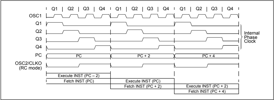
The microcontroller clock input, whether from an internal or external source, is internally divided by four to generate four non-overlapping quadrature clocks (Q1, Q2, Q3 and Q4). Internally, the program counter is incremented on every Q1; the instruction is fetched from the program memory and latched into the Instruction Register (IR) during Q4. The instruction is decoded and executed during the following Q1 through Q4. The clocks and instruction execution flow are shown in Figure 5-3.
5.2.2 INSTRUCTION FLOW/PIPELINING
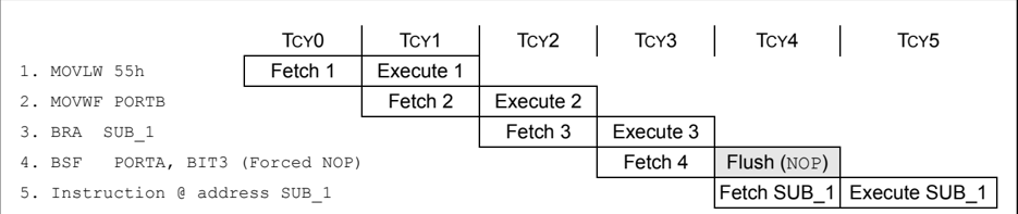
An “Instruction Cycle” consists of four Q cycles: Q1 through Q4. The instruction fetch and execute are pipelined in such a manner that a fetch takes one instruction cycle, while the decode and execute takes another instruction cycle. However, due to the pipelining, each instruction effectively executes in one cycle. If an instruction causes the program counter to change (e.g., GOTO), then two cycles are required to complete the instruction (Example 5-3).
A fetch cycle begins with the Program Counter (PC) incrementing in Q1.
In the execution cycle, the fetched instruction is latched into the Instruction Register (IR) in cycle Q1. This instruction is then decoded and executed during the Q2, Q3 and Q4 cycles. Data memory is read during Q2 (operand read) and written during Q4 (destination write).
FIGURE 5-3: CLOCK/INSTRUCTION CYCLE
EXAMPLE 5-3: INSTRUCTION PIPELINE FLOW
| Tcy0 | Tcy1 | Tcy2 | Tcy3 | Tcy4 | Tcy5 | |
|---|---|---|---|---|---|---|
| 1. MOVLW 55h | Fetch 1 | Execute 1 | ||||
| 2. MOVWF PORTB | Fetch 2 | Execute 2 | ||||
| 3. BRA SUB_1 | Fetch 3 | Execute 3 | ||||
| 4. BSF PORTA, BIT3 (Forced NOP) | Fetch 4 | Flush (NOP) | ||||
| 5. Instruction @ address SUB_1 | Fetch SUB_1 | Execute SUB_1 |
Note: All instructions are single cycle, except for any program branches. These take two cycles since the fetch instruction is “flushed” from the pipeline while the new instruction is being fetched and then executed.
5.2.3 INSTRUCTIONS IN PROGRAM MEMORY
The program memory is addressed in bytes. Instructions are stored as two bytes or four bytes in program memory. The Least Significant Byte of an instruction word is always stored in a program memory location with an even address (LSb = 0). To maintain alignment with instruction boundaries, the PC increments in steps of 2 and the LSb will always read ‘0’ (see Section 5.1.1 “Program Counter”).
Figure 5-4 shows an example of how instruction words are stored in the program memory.
The CALL and GOTO instructions have the absolute program memory address embedded into the instruction. Since instructions are always stored on word boundaries, the data contained in the instruction is a word address. The word address is written to PC<20:1>, which accesses the desired byte address in program memory. Instruction #2 in Figure 5-4 shows how the instruction, GOTO 0006h, is encoded in the program memory. Program branch instructions, which encode a relative address offset, operate in the same manner. The offset value stored in a branch instruction represents the number of single-word instructions that the PC will be offset by. Section 26.0 “Instruction Set Summary” provides further details of the instruction set.
FIGURE 5-4: INSTRUCTIONS IN PROGRAM MEMORY
| Program Memory Byte Locations → | LSB = 1 | LSB = 0 | Word Address ↓ |
|---|---|---|---|
| Instruction 1: MOVLW 055h | 0Fh | 55h | 000008h |
| Instruction 2: GOTO 0006h | EFh | 03h | 00000Ah |
| F0h | 00h | 00000Ch | |
| Instruction 3: MOVFF 123h, 456h | C1h | 23h | 00000Eh |
| F4h | 56h | 000010h | |
| 000012h | |||
| 000014h |
5.2.4 TWO-WORD INSTRUCTIONS
The standard PIC18 instruction set has four two-word instructions: CALL, MOVFF, GOTO and LSFR. In all cases, the second word of the instructions always has ‘1111’ as its four Most Significant bits; the other 12 bits are literal data, usually a data memory address.
The use of ‘1111’ in the 4 MSbs of an instruction specifies a special form of NOP. If the instruction is executed in proper sequence, immediately after the first word, the data in the second word is accessed and used by the instruction sequence. If the first word is skipped for some reason and the second word is executed by itself, a NOP is executed instead. This is necessary for cases when the two-word instruction is preceded by a conditional instruction that changes the PC. Example 5-4 shows how this works.
Note: See Section 5.5 “Program Memory and the Extended Instruction Set” for information on two-word instruction in the extended instruction set.
EXAMPLE 5-4: TWO-WORD INSTRUCTIONS
CASE 1:
| Object Code | Source Code |
|---|---|
| 0110 0110 0000 0000 | TSTFSZ REG1 ; is RAM location 0? |
| 1100 0001 0010 0011 | MOVFF REG1, REG2 ; No, skip this word |
| 1111 0100 0101 0110 | ; Execute this word as a NOP |
| 0010 0100 0000 0000 | ADDWF REG3 ; continue code |
CASE 2:
| Object Code | Source Code |
|---|---|
| 0110 0110 0000 0000 | TSTFSZ REG1 ; is RAM location 0? |
| 1100 0001 0010 0011 | MOVFF REG1, REG2 ; Yes, execute this word |
| 1111 0100 0101 0110 | ; 2nd word of instruction |
| 0010 0100 0000 0000 | ADDWF REG3 ; continue code |
5.3 Data Memory Organization
Note: The operation of some aspects of data memory are changed when the PIC18 extended instruction set is enabled. See Section 5.6 “Data Memory and the Extended Instruction Set” for more information.
The data memory in PIC18 devices is implemented as static RAM. Each register in the data memory has a 12-bit address, allowing up to 4096 bytes of data memory. The memory space is divided into as many as 16 banks that contain 256 bytes each. PIC18F2455/2550/4455/4550 devices implement eight complete banks, for a total of 2048 bytes. Figure 5-5 shows the data memory organization for the devices.
The data memory contains Special Function Registers (SFRs) and General Purpose Registers (GPRs). The SFRs are used for control and status of the controller and peripheral functions, while GPRs are used for data storage and scratchpad operations in the user’s application. Any read of an unimplemented location will read as ‘0’s.
The instruction set and architecture allow operations across all banks. The entire data memory may be accessed by Direct, Indirect or Indexed Addressing modes. Addressing modes are discussed later in this subsection.
To ensure that commonly used registers (SFRs and select GPRs) can be accessed in a single cycle, PIC18 devices implement an Access Bank. This is a 256-byte memory space that provides fast access to SFRs and the lower portion of GPR Bank 0 without using the BSR. Section 5.3.3 “Access Bank” provides a detailed description of the Access RAM.
5.3.1 USB RAM
Banks 4 through 7 of the data memory are actually mapped to special dual port RAM. When the USB module is disabled, the GPRs in these banks are used like any other GPR in the data memory space.
When the USB module is enabled, the memory in these banks is allocated as buffer RAM for USB operation. This area is shared between the microcontroller core and the USB Serial Interface Engine (SIE) and is used to transfer data directly between the two.
It is theoretically possible to use the areas of USB RAM that are not allocated as USB buffers for normal scratchpad memory or other variable storage. In practice, the dynamic nature of buffer allocation makes this risky at best. Additionally, Bank 4 is used for USB buffer management when the module is enabled and should not be used for any other purposes during that time.
Additional information on USB RAM and buffer operation is provided in Section 17.0 “Universal Serial Bus (USB)”.
5.3.2 BANK SELECT REGISTER (BSR)
Large areas of data memory require an efficient addressing scheme to make rapid access to any address possible. Ideally, this means that an entire address does not need to be provided for each read or write operation. For PIC18 devices, this is accomplished with a RAM banking scheme. This divides the memory space into 16 contiguous banks of 256 bytes. Depending on the instruction, each location can be addressed directly by its full 12-bit address, or an 8-bit low-order address and a 4-bit Bank Pointer.
Most instructions in the PIC18 instruction set make use of the Bank Pointer, known as the Bank Select Register (BSR). This SFR holds the 4 Most Significant bits of a location’s address; the instruction itself includes the eight Least Significant bits. Only the four lower bits of the BSR are implemented (BSR3:BSR0). The upper four bits are unused; they will always read ‘0’ and cannot be written to. The BSR can be loaded directly by using the MOVLB instruction.
The value of the BSR indicates the bank in data memory. The eight bits in the instruction show the location in the bank and can be thought of as an offset from the bank’s lower boundary. The relationship between the BSR’s value and the bank division in data memory is shown in Figure 5-6.
Since up to sixteen registers may share the same low-order address, the user must always be careful to ensure that the proper bank is selected before performing a data read or write. For example, writing what should be program data to an 8-bit address of F9h, while the BSR is 0Fh, will end up resetting the program counter.
While any bank can be selected, only those banks that are actually implemented can be read or written to. Writes to unimplemented banks are ignored, while reads from unimplemented banks will return ‘0’s. Even so, the STATUS register will still be affected as if the operation was successful. The data memory map in Figure 5-5 indicates which banks are implemented.
In the core PIC18 instruction set, only the MOVFF instruction fully specifies the 12-bit address of the source and target registers. This instruction ignores the BSR completely when it executes. All other instructions include only the low-order address as an operand and must use either the BSR or the Access Bank to locate their target registers.
FIGURE 5-5: DATA MEMORY MAP
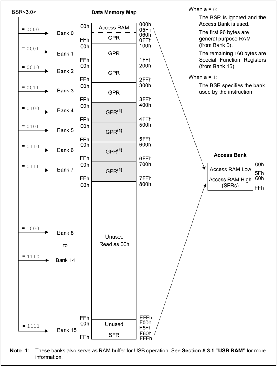
Note 1: These banks also serve as RAM buffer for USB operation. See Section 5.3.1 “USB RAM” for more information.
FIGURE 5-6: USE OF THE BANK SELECT REGISTER (DIRECT ADDRESSING)
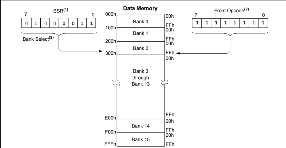
Note 1: The Access RAM bit of the instruction can be used to force an override of the selected bank (BSR<3:0>) to the registers of the Access Bank. 2: The MOVFF instruction embeds the entire 12-bit address in the instruction.
5.3.3 ACCESS BANK
While the use of the BSR, with an embedded 8-bit address, allows users to address the entire range of data memory, it also means that the user must always ensure that the correct bank is selected. Otherwise, data may be read from or written to the wrong location. This can be disastrous if a GPR is the intended target of an operation but an SFR is written to instead. Verifying and/or changing the BSR for each read or write to data memory can become very inefficient.
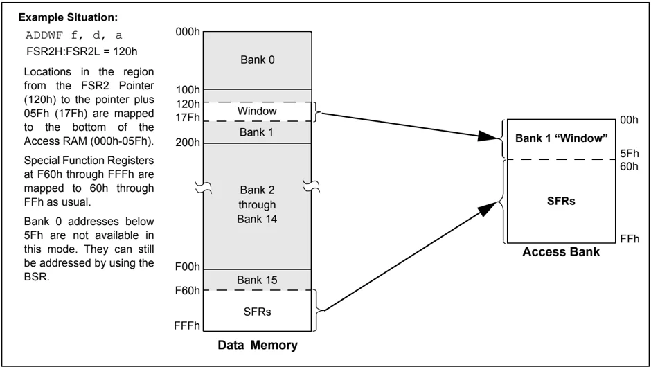
To streamline access for the most commonly used data memory locations, the data memory is configured with an Access Bank, which allows users to access a mapped block of memory without specifying a BSR. The Access Bank consists of the first 96 bytes of memory (00h-5Fh) in Bank 0 and the last 160 bytes of memory (60h-FFh) in Block 15. The lower half is known as the "Access RAM" and is composed of GPRs. The upper half is where the device's SFRs are mapped. These two areas are mapped contiguously in the Access Bank and can be addressed in a linear fashion by an 8-bit address (Figure 5-5).
The Access Bank is used by core PIC18 instructions that include the Access RAM bit (the 'a' parameter in the instruction). When 'a' is equal to '1', the instruction uses the BSR and the 8-bit address included in the opcode for the data memory address. When 'a' is '0', however, the instruction is forced to use the Access Bank address map; the current value of the BSR is ignored entirely.
Using this "forced" addressing allows the instruction to operate on a data address in a single cycle without updating the BSR first. For 8-bit addresses of 60h and above, this means that users can evaluate and operate on SFRs more efficiently. The Access RAM below 60h is a good place for data values that the user might need to access rapidly, such as immediate computational results or common program variables. Access RAM also allows for faster and more code efficient context saving and switching of variables.
The mapping of the Access Bank is slightly different when the extended instruction set is enabled (XINST Configuration bit = 1). This is discussed in more detail in Section 5.6.3 "Mapping the Access Bank in Indexed Literal Offset Mode".
5.3.4 GENERAL PURPOSE REGISTER FILE
PIC18 devices may have banked memory in the GPR area. This is data RAM which is available for use by all instructions. GPRs start at the bottom of Bank 0 (address 000h) and grow upwards towards the bottom of the SFR area. GPRs are not initialized by a Power-on Reset and are unchanged on all other Resets.
5.3.5 SPECIAL FUNCTION REGISTERS
The Special Function Registers (SFRs) are registers used by the CPU and peripheral modules for controlling the desired operation of the device. These registers are implemented as static RAM in the data memory space. SFRs start at the top of data memory and extend downward to occupy the top segment of Bank 15, from F60h to FFFh. A list of these registers is given in Table 5-1 and Table 5-2.
The SFRs can be classified into two sets: those associated with the “core” device functionality (ALU, Resets and interrupts) and those related to the peripheral functions. The Reset and interrupt registers are described in their respective chapters, while the ALU’s STATUS register is described later in this section. Registers related to the operation of a peripheral feature are described in the chapter for that peripheral.
The SFRs are typically distributed among the peripherals whose functions they control. Unused SFR locations are unimplemented and read as ‘0’s.
TABLE 5-1: SPECIAL FUNCTION REGISTER MAP
| Address | Name | Address | Name | Address | Name | Address | Name | Address | Name |
|---|---|---|---|---|---|---|---|---|---|
| FFFh | TOSU | FDFh | INDF2(1) | FBFh | CCPR1H | F9Fh | IPR1 | F7Fh | UEP15 |
| FFEh | TOSH | FDEh | POSTINC2(1) | FBEh | CCPR1L | F9Eh | PIR1 | F7Eh | UEP14 |
| FFDh | TOSL | FDDh | POSTDEC2(1) | FBDh | CCP1CON | F9Dh | PIE1 | F7Dh | UEP13 |
| FFCb | STKPTR | FDCb | PREINC2(1) | FBCb | CCPR2H | F9Cb | —(2) | F7Cb | UEP12 |
| FFBh | PCLATU | FDBh | PLUSW2(1) | FBBh | CCPR2L | F9Bh | OSCTUNE | F7Bh | UEP11 |
| FFAh | PCLATH | FDAh | FSR2H | FBAh | CCP2CON | F9Ah | —(2) | F7Ah | UEP10 |
| FF9h | PCL | FD9h | FSR2L | FB9h | —(2) | F99h | —(2) | F79h | UEP9 |
| FF8h | TBLPTRU | FD8h | STATUS | FB8h | BAUDCON | F98h | —(2) | F78h | UEP8 |
| FF7h | TBLPTRH | FD7h | TMR0H | FB7h | ECCP1DEL | F97h | —(2) | F77h | UEP7 |
| FF6h | TBLPTRL | FD6h | TMR0L | FB6h | ECCP1AS | F96h | TRISE(3) | F76h | UEP6 |
| FF5h | TABLAT | FD5h | T0CON | FB5h | CVRCON | F95h | TRISD(3) | F75h | UEP5 |
| FF4h | PRODH | FD4h | —(2) | FB4h | CMCON | F94h | TRISC | F74h | UEP4 |
| FF3h | PRODL | FD3h | OSCCON | FB3h | TMR3H | F93h | TRISB | F73h | UEP3 |
| FF2h | INTCON | FD2h | HLVDCON | FB2h | TMR3L | F92h | TRISA | F72h | UEP2 |
| FF1h | INTCON2 | FD1h | WDTCON | FB1h | T3CON | F91h | —(2) | F71h | UEP1 |
| FF0h | INTCON3 | FD0h | RCON | FB0h | SPBRGH | F90h | —(2) | F70h | UEP0 |
| FEFh | INDF0(1) | FCFh | TMR1H | FAh | SPBRG | F8Fh | —(2) | F6Fh | UCFG |
| FEEh | POSTINC0(1) | FCEh | TMR1L | FAEh | RCREG | F8Eh | —(2) | F6Eh | UADDR |
| FEDh | POSTDEC0(1) | FCDh | T1CON | FADh | TXREG | F8Dh | LATE(3) | F6Dh | UCON |
| FECb | PREINC0(1) | FCCb | TMR2 | FACb | TXSTA | F8Cb | LATD(3) | F6Cb | USTAT |
| FEBh | PLUSW0(1) | FCBh | PR2 | FABh | RCSTA | F8Bh | LATC | F6Bh | UEIE |
| FEAh | FSR0H | FCAh | T2CON | FAAh | —(2) | F8Ah | LATB | F6Ah | UEIR |
| FE9h | FSR0L | FC9h | SSPBUF | FA9h | EEADR | F89h | LATA | F69h | UIE |
| FE8h | WREG | FC8h | SSPADD | FA8h | EEDATA | F88h | —(2) | F68h | UIR |
| FE7h | INDF1(1) | FC7h | SSPSTAT | FA7h | EECON2(1) | F87h | —(2) | F67h | UFRMH |
| FE6h | POSTINC1(1) | FC6h | SSPCON1 | FA6h | EECON1 | F86h | —(2) | F66h | UFRML |
| FE5h | POSTDEC1(1) | FC5h | SSPCON2 | FA5h | —(2) | F85h | —(2) | F65h | SPPCON(3) |
| FE4h | PREINC1(1) | FC4h | ADRESH | FA4h | —(2) | F84h | PORTE | F64h | SPPEPS(3) |
| FE3h | PLUSW1(1) | FC3h | ADRESL | FA3h | —(2) | F83h | PORTD(3) | F63h | SPPCFG(3) |
| FE2h | FSR1H | FC2h | ADCON0 | FA2h | IPR2 | F82h | PORTC | F62h | SPPDATA(3) |
| FE1h | FSR1L | FC1h | ADCON1 | FA1h | PIR2 | F81h | PORTB | F61h | —(2) |
| FE0h | BSR | FC0h | ADCON2 | FA0h | PIE2 | F80h | PORTA | F60h | —(2) |
Note 1: Not a physical register.
2: Unimplemented registers are read as ‘0’.
3: These registers are implemented only on 40/44-pin devices.
TABLE 5-2: REGISTER FILE SUMMARY
| File Name | Bit 7 | Bit 6 | Bit 5 | Bit 4 | Bit 3 | Bit 2 | Bit 1 | Bit 0 | Value on POR, BOR | Details on page |
|---|---|---|---|---|---|---|---|---|---|---|
| TOSU | — | — | — | Top-of-Stack Upper Byte (TOS<20:16>) | — | — | — | — | ---0 0000 | 53, 60 |
| TOSH | Top-of-Stack High Byte (TOS<15:8>) | — | — | — | — | — | — | — | 0000 0000 | 53, 60 |
| TOSL | Top-of-Stack Low Byte (TOS<7:0>) | — | — | — | — | — | — | — | 0000 0000 | 53, 60 |
| STKPTR | STKFUL | STKUNF | — | SP4 | SP3 | SP2 | SP1 | SP0 | 00-0 0000 | 53, 61 |
| PCLATU | — | — | — | Holding Register for PC<20:16> | — | — | — | — | ---0 0000 | 53, 60 |
| PCLATH | Holding Register for PC<15:8> | — | — | — | — | — | — | — | 0000 0000 | 53, 60 |
| PCL | PC Low Byte (PC<7:0>) | — | — | — | — | — | — | — | 0000 0000 | 53, 60 |
| TBLPTRU | — | — | bit 21(1) | Program Memory Table Pointer Upper Byte (TBLPTR<20:16>) | — | — | — | — | --00 0000 | 53, 84 |
| TBLPTRH | Program Memory Table Pointer High Byte (TBLPTR<15:8>) | — | — | — | — | — | — | — | 0000 0000 | 53, 84 |
| TBLPTRL | Program Memory Table Pointer Low Byte (TBLPTR<7:0>) | — | — | — | — | — | — | — | 0000 0000 | 53, 84 |
| TABLAT | Program Memory Table Latch | — | — | — | — | — | — | — | 0000 0000 | 53, 84 |
| PRODH | Product Register High Byte | — | — | — | — | — | — | — | xxxx xxxx | 53, 97 |
| PRODL | Product Register Low Byte | — | — | — | — | — | — | — | xxxx xxxx | 53, 97 |
| INTCON | GIE/GIEH | PEIE/GIEL | TMR0IE | INT0IE | RBIE | TMR0IF | INT0IF | RBIF | 0000 000x | 53, 101 |
| INTCON2 | RBPU | INTEDG0 | INTEDG1 | INTEDG2 | — | TMR0IP | — | RBIP | 1111 -1-1 | 53, 102 |
| INTCON3 | INT2IP | INT1IP | — | INT2IE | INT1IE | — | INT2IF | INT1IF | 11-0 0-00 | 53, 103 |
| INDF0 | Uses contents of FSR0 to address data memory – value of FSR0 not changed (not a physical register) | — | — | — | — | — | — | — | N/A | 53, 75 |
| POSTINC0 | Uses contents of FSR0 to address data memory – value of FSR0 post-incremented (not a physical register) | — | — | — | — | — | — | — | N/A | 53, 76 |
| POSTDEC0 | Uses contents of FSR0 to address data memory – value of FSR0 post-decremented (not a physical register) | — | — | — | — | — | — | — | N/A | 53, 76 |
| PREINC0 | Uses contents of FSR0 to address data memory – value of FSR0 pre-incremented (not a physical register) | — | — | — | — | — | — | — | N/A | 53, 76 |
| PLUSW0 | Uses contents of FSR0 to address data memory – value of FSR0 pre-incremented (not a physical register) – value of FSR0 offset by W | — | — | — | — | — | — | — | N/A | 53, 76 |
| FSR0H | — | — | — | — | Indirect Data Memory Address Pointer 0 High Byte | — | — | — | ---- 0000 | 53, 75 |
| FSR0L | Indirect Data Memory Address Pointer 0 Low Byte | — | — | — | — | — | — | — | xxxx xxxx | 53, 75 |
| WREG | Working Register | — | — | — | — | — | — | — | xxxx xxxx | 53 |
| INDF1 | Uses contents of FSR1 to address data memory – value of FSR1 not changed (not a physical register) | — | — | — | — | — | — | — | N/A | 53, 75 |
| POSTINC1 | Uses contents of FSR1 to address data memory – value of FSR1 post-incremented (not a physical register) | — | — | — | — | — | — | — | N/A | 53, 76 |
| POSTDEC1 | Uses contents of FSR1 to address data memory – value of FSR1 post-decremented (not a physical register) | — | — | — | — | — | — | — | N/A | 53, 76 |
| PREINC1 | Uses contents of FSR1 to address data memory – value of FSR1 pre-incremented (not a physical register) | — | — | — | — | — | — | — | N/A | 53, 76 |
| PLUSW1 | Uses contents of FSR1 to address data memory – value of FSR1 pre-incremented (not a physical register) – value of FSR1 offset by W | — | — | — | — | — | — | — | N/A | 53, 76 |
| FSR1H | — | — | — | — | Indirect Data Memory Address Pointer 1 High Byte | — | — | — | ---- 0000 | 53, 75 |
| FSR1L | Indirect Data Memory Address Pointer 1 Low Byte | — | — | — | — | — | — | — | xxxx xxxx | 53, 75 |
| BSR | — | — | — | — | Bank Select Register | — | — | — | ---- 0000 | 54, 65 |
| INDF2 | Uses contents of FSR2 to address data memory – value of FSR2 not changed (not a physical register) | — | — | — | — | — | — | — | N/A | 54, 75 |
| POSTINC2 | Uses contents of FSR2 to address data memory – value of FSR2 post-incremented (not a physical register) | — | — | — | — | — | — | — | N/A | 54, 76 |
| POSTDEC2 | Uses contents of FSR2 to address data memory – value of FSR2 post-decremented (not a physical register) | — | — | — | — | — | — | — | N/A | 54, 76 |
| PREINC2 | Uses contents of FSR2 to address data memory – value of FSR2 pre-incremented (not a physical register) | — | — | — | — | — | — | — | N/A | 54, 76 |
| PLUSW2 | Uses contents of FSR2 to address data memory – value of FSR2 pre-incremented (not a physical register) – value of FSR2 offset by W | — | — | — | — | — | — | — | N/A | 54, 76 |
| FSR2H | — | — | — | — | Indirect Data Memory Address Pointer 2 High Byte | — | — | — | ---- 0000 | 54, 75 |
| FSR2L | Indirect Data Memory Address Pointer 2 Low Byte | — | — | — | — | — | — | — | xxxx xxxx | 54, 75 |
| STATUS | — | — | — | N | OV | Z | DC | C | ---x xxxx | 54, 73 |
| TMR0H | Timer0 Register High Byte | — | — | — | — | — | — | — | 0000 0000 | 54, 129 |
| TMR0L | Timer0 Register Low Byte | — | — | — | — | — | — | — | xxxx xxxx | 54, 129 |
| T0CON | TMR0ON | T08BIT | T0CS | T0SE | PSA | T0PS2 | T0PS1 | T0PS0 | 1111 1111 | 54, 127 |
Legend: x = unknown, u = unchanged, - = unimplemented, q = value depends on condition. Shaded cells are unimplemented, read as ‘0’.
Note 1: Bit 21 of the TBLPTRU allows access to the device Configuration bits.
2: The SBOREN bit is only available when BOREN<1:0> = 01; otherwise, the bit reads as ‘0’.
3: These registers and/or bits are not implemented on 28-pin devices and are read as ‘0’. Reset values are shown for 40/44-pin devices; individual unimplemented bits should be interpreted as ‘-’.
4: RA6 is configured as a port pin based on various primary oscillator modes. When the port pin is disabled, all of the associated bits read ‘0’.
5: RE3 is only available as a port pin when the MCLRE Configuration bit is clear; otherwise, the bit reads as ‘0’.
6: RC5 and RC4 are only available as port pins when the USB module is disabled (UCON<3> = 0).
7: I²C™ Slave mode only.
TABLE 5-2: REGISTER FILE SUMMARY (CONTINUED)
| File Name | Bit 7 | Bit 6 | Bit 5 | Bit 4 | Bit 3 | Bit 2 | Bit 1 | Bit 0 | Value on POR, BOR | Details on page |
|---|---|---|---|---|---|---|---|---|---|---|
| OSCCON | IDLEN | IRCF2 | IRCF1 | IRCF0 | OSTS | IOFS | SCS1 | SCS0 | 0100 q000 | 54, 33 |
| HLVDCON | VDIRMAG | — | IRVST | HLVDEN | HLVDL3 | HLVDL2 | HLVDL1 | HLVDL0 | 0-00 0101 | 54, 285 |
| WDTCON | — | — | — | — | — | — | — | SWDTEN | --- ---0 | 54, 304 |
| RCON | IPEN | SBOREN(2) | — | RI | TO | PD | POR | BOR | 0q-1 11q0 | 54, 46 |
| TMR1H | Timer1 Register High Byte | xxxx xxxx | 54, 136 | |||||||
| TMR1L | Timer1 Register Low Byte | xxxx xxxx | 54, 136 | |||||||
| T1CON | RD16 | T1RUN | T1CKPS1 | T1CKPS0 | T1OSCEN | T1SYNC | TMR1CS | TMR1ON | 0000 0000 | 54, 131 |
| TMR2 | Timer2 Register | 0000 0000 | 54, 138 | |||||||
| PR2 | Timer2 Period Register | 1111 1111 | 54, 138 | |||||||
| T2CON | — | T2OUTPS3 | T2OUTPS2 | T2OUTPS1 | T2OUTPS0 | TMR2ON | T2CKPS1 | T2CKPS0 | -000 0000 | 54, 137 |
| SSPBUF | MSSP Receive Buffer/Transmit Register | xxxx xxxx | 54, 198, 207 | |||||||
| SSPADD | MSSP Address Register in I²C™ Slave mode. MSSP Baud Rate Reload Register in I²C™ Master mode. | 0000 0000 | 54, 207 | |||||||
| SSPSTAT | SMP | CKE | D/A | P | S | R/W | UA | BF | 0000 0000 | 54, 198, 208 |
| SSPCON1 | WCOL | SSPOV | SSPEN | CKP | SSPM3 | SSPM2 | SSPM1 | SSPM0 | 0000 0000 | 54, 199, 209 |
| SSPCON2 | GCEN | ACKSTAT | ACKDT/ADMSK5(7) | ACKEN/ADMSK4(7) | RCEN/ADMSK3(7) | PEN/ADMSK2(7) | RSEN/ADMSK1(7) | SEN | 0000 0000 | 54, 210 |
| ADRESH | A/D Result Register High Byte | xxxx xxxx | 54, 274 | |||||||
| ADRESL | A/D Result Register Low Byte | xxxx xxxx | 54, 274 | |||||||
| ADCON0 | — | — | CHS3 | CHS2 | CHS1 | CHS0 | GO/DONE | ADON | --00 0000 | 54, 265 |
| ADCON1 | — | — | VCFG1 | VCFG0 | PCFG3 | PCFG2 | PCFG1 | PCFG0 | --00 0qqq | 54, 266 |
| ADCON2 | ADFM | — | ACQT2 | ACQT1 | ACQT0 | ADCS2 | ADCS1 | ADCS0 | 0-00 0000 | 54, 267 |
| CCPR1H | Capture/Compare/PWM Register 1 High Byte | xxxx xxxx | 55, 144 | |||||||
| CCPR1L | Capture/Compare/PWM Register 1 Low Byte | xxxx xxxx | 55, 144 | |||||||
| CCP1CON | P1M1(3) | P1M0(3) | DC1B1 | DC1B0 | CCP1M3 | CCP1M2 | CCP1M1 | CCP1M0 | 0000 0000 | 55, 143, 151 |
| CCPR2H | Capture/Compare/PWM Register 2 High Byte | xxxx xxxx | 55, 144 | |||||||
| CCPR2L | Capture/Compare/PWM Register 2 Low Byte | xxxx xxxx | 55, 144 | |||||||
| CCP2CON | — | — | DC2B1 | DC2B0 | CCP2M3 | CCP2M2 | CCP2M1 | CCP2M0 | --00 0000 | 55, 143 |
| BAUDCON | ABDOVF | RCIDL | RXDTP | TXCKP | BRG16 | — | WUE | ABDEN | 0100 0-00 | 55, 246 |
| ECCP1DEL | PRSEN | PDC6(3) | PDC5(3) | PDC4(3) | PDC3(3) | PDC2(3) | PDC1(3) | PDC0(3) | 0000 0000 | 55, 160 |
| ECCP1AS | ECCPASE | ECCPAS2 | ECCPAS1 | ECCPAS0 | PSSAC1 | PSSAC0 | PSSBD1(3) | PSSBD0(3) | 0000 0000 | 55, 161 |
| CVRCON | CVREN | CVROE | CVRR | CVRSS | CVR3 | CVR2 | CVR1 | CVR0 | 0000 0000 | 55, 281 |
| CMCON | C2OUT | C1OUT | C2INV | C1INV | CIS | CM2 | CM1 | CM0 | 0000 0111 | 55, 275 |
| TMR3H | Timer3 Register High Byte | xxxx xxxx | 55, 141 | |||||||
| TMR3L | Timer3 Register Low Byte | xxxx xxxx | 55, 141 | |||||||
| T3CON | RD16 | T3CCP2 | T3CKPS1 | T3CKPS0 | T3CCP1 | T3SYNC | TMR3CS | TMR3ON | 0000 0000 | 55, 139 |
| SPBRGH | EUSART Baud Rate Generator Register High Byte | 0000 0000 | 55, 247 | |||||||
| SPBRG | EUSART Baud Rate Generator Register Low Byte | 0000 0000 | 55, 247 | |||||||
| RCREG | EUSART Receive Register | 0000 0000 | 55, 256 | |||||||
| TXREG | EUSART Transmit Register | 0000 0000 | 55, 253 | |||||||
| TXSTA | CSRC | TX9 | TXEN | SYNC | SENDB | BRGH | TRMT | TX9D | 0000 0010 | 55, 244 |
| RCSTA | SPEN | RX9 | SREN | CREN | ADDEN | FERR | OERR | RX9D | 0000 000x | 55, 245 |
Legend: x = unknown, u = unchanged, - = unimplemented, q = value depends on condition. Shaded cells are unimplemented, read as ‘0’.
Note 1: Bit 21 of the TBLPTRU allows access to the device Configuration bits.
Note 2: The SBOREN bit is only available when BOREN<1:0> = 01; otherwise, the bit reads as ‘0’.
Note 3: These registers and/or bits are not implemented on 28-pin devices and are read as ‘0’. Reset values are shown for 40/44-pin devices; individual unimplemented bits should be interpreted as ‘-’.
Note 4: RA6 is configured as a port pin based on various primary oscillator modes. When the port pin is disabled, all of the associated bits read ‘0’.
Note 5: RE3 is only available as a port pin when the MCLRE Configuration bit is clear; otherwise, the bit reads as ‘0’.
Note 6: RC5 and RC4 are only available as port pins when the USB module is disabled (UCON<3> = 0).
Note 7: I²C™ Slave mode only.
TABLE 5-2: REGISTER FILE SUMMARY (CONTINUED)
| File Name | Bit 7 | Bit 6 | Bit 5 | Bit 4 | Bit 3 | Bit 2 | Bit 1 | Bit 0 | Value on POR, BOR | Details on page |
|---|---|---|---|---|---|---|---|---|---|---|
| EEADR | EEPROM Address Register | 0000 0000 | 55, 91 | |||||||
| EEDATA | EEPROM Data Register | 0000 0000 | 55, 91 | |||||||
| EECON2 | EEPROM Control Register 2 (not a physical register) | 0000 0000 | 55, 82 | |||||||
| EECON1 | EEPGD | CFGS | — | FREE | WRERR | WREN | WR | RD | xx-0 x000 | 55, 83 |
| IPR2 | OSCFIP | CMIP | USBIP | EEIP | BCLIP | HLVDIP | TMR3IP | CCP2IP | 1111 1111 | 56, 109 |
| PIR2 | OSCFIF | CMIF | USBIF | EEIF | BCLIF | HLVDIF | TMR3IF | CCP2IF | 0000 0000 | 56, 105 |
| PIE2 | OSCFIE | CMIE | USBIE | EEIE | BCLIE | HLVDIE | TMR3IE | CCP2IE | 0000 0000 | 56, 107 |
| IPR1 | SPPIP(3) | ADIP | RCIP | TXIP | SSPIP | CCP1IP | TMR2IP | TMR1IP | 1111 1111 | 56, 108 |
| PIR1 | SPPIF(3) | ADIF | RCIF | TXIF | SSPIF | CCP1IF | TMR2IF | TMR1IF | 0000 0000 | 56, 104 |
| PIE1 | SPPIE(3) | ADIE | RCIE | TXIE | SSPIE | CCP1IE | TMR2IE | TMR1IE | 0000 0000 | 56, 106 |
| OSCTUNE | INTSRC | — | — | TUN4 | TUN3 | TUN2 | TUN1 | TUN0 | 0--0 0000 | 56, 28 |
| TRISE(3) | — | — | — | — | — | TRISE2 | TRISE1 | TRISE0 | ---- -111 | 56, 126 |
| TRISD(3) | TRISD7 | TRISD6 | TRISD5 | TRISD4 | TRISD3 | TRISD2 | TRISD1 | TRISD0 | 1111 1111 | 56, 124 |
| TRISC | TRISC7 | TRISC6 | — | — | — | TRISC2 | TRISC1 | TRISC0 | 11-- -111 | 56, 121 |
| TRISB | TRISB7 | TRISB6 | TRISB5 | TRISB4 | TRISB3 | TRISB2 | TRISB1 | TRISB0 | 1111 1111 | 56, 118 |
| TRISA | — | TRISA6(4) | TRISA5 | TRISA4 | TRISA3 | TRISA2 | TRISA1 | TRISA0 | -111 1111 | 56, 115 |
| LATE(3) | — | — | — | — | — | LATE2 | LATE1 | LATE0 | ---- -xxx | 56, 126 |
| LATD(3) | LATD7 | LATD6 | LATD5 | LATD4 | LATD3 | LATD2 | LATD1 | LATD0 | xxxx xxxx | 56, 124 |
| LATC | LATC7 | LATC6 | — | — | — | LATC2 | LATC1 | LATC0 | xx-- -xxx | 56, 121 |
| LATB | LATB7 | LATB6 | LATB5 | LATB4 | LATB3 | LATB2 | LATB1 | LATB0 | xxxx xxxx | 56, 118 |
| LATA | — | LATA6(4) | LATA5 | LATA4 | LATA3 | LATA2 | LATA1 | LATA0 | -xxx xxxx | 56, 115 |
| PORTE | RDPU(3) | — | — | — | RE3(5) | RE2(3) | RE1(3) | RE0(3) | 0--- x000 | 56, 125 |
| PORTD(3) | RD7 | RD6 | RD5 | RD4 | RD3 | RD2 | RD1 | RD0 | xxxx xxxx | 56, 124 |
| PORTC | RC7 | RC6 | RC5(6) | RC4(6) | — | RC2 | RC1 | RC0 | xxxx -xxx | 56, 121 |
| PORTB | RB7 | RB6 | RB5 | RB4 | RB3 | RB2 | RB1 | RB0 | xxxx xxxx | 56, 118 |
| PORTA | — | RA6(4) | RA5 | RA4 | RA3 | RA2 | RA1 | RA0 | -x0x 0000 | 56, 115 |
| UEP15 | — | — | — | EPHSHK | EPCONDIS | EPOUTEN | EPINEN | EPSTALL | ---0 0000 | 57, 172 |
| UEP14 | — | — | — | EPHSHK | EPCONDIS | EPOUTEN | EPINEN | EPSTALL | ---0 0000 | 57, 172 |
| UEP13 | — | — | — | EPHSHK | EPCONDIS | EPOUTEN | EPINEN | EPSTALL | ---0 0000 | 57, 172 |
| UEP12 | — | — | — | EPHSHK | EPCONDIS | EPOUTEN | EPINEN | EPSTALL | ---0 0000 | 57, 172 |
| UEP11 | — | — | — | EPHSHK | EPCONDIS | EPOUTEN | EPINEN | EPSTALL | ---0 0000 | 57, 172 |
| UEP10 | — | — | — | EPHSHK | EPCONDIS | EPOUTEN | EPINEN | EPSTALL | ---0 0000 | 57, 172 |
| UEP9 | — | — | — | EPHSHK | EPCONDIS | EPOUTEN | EPINEN | EPSTALL | ---0 0000 | 57, 172 |
| UEP8 | — | — | — | EPHSHK | EPCONDIS | EPOUTEN | EPINEN | EPSTALL | ---0 0000 | 57, 172 |
| UEP7 | — | — | — | EPHSHK | EPCONDIS | EPOUTEN | EPINEN | EPSTALL | ---0 0000 | 57, 172 |
| UEP6 | — | — | — | EPHSHK | EPCONDIS | EPOUTEN | EPINEN | EPSTALL | ---0 0000 | 57, 172 |
| UEP5 | — | — | — | EPHSHK | EPCONDIS | EPOUTEN | EPINEN | EPSTALL | ---0 0000 | 57, 172 |
| UEP4 | — | — | — | EPHSHK | EPCONDIS | EPOUTEN | EPINEN | EPSTALL | ---0 0000 | 57, 172 |
| UEP3 | — | — | — | EPHSHK | EPCONDIS | EPOUTEN | EPINEN | EPSTALL | ---0 0000 | 57, 172 |
| UEP2 | — | — | — | EPHSHK | EPCONDIS | EPOUTEN | EPINEN | EPSTALL | ---0 0000 | 57, 172 |
| UEP1 | — | — | — | EPHSHK | EPCONDIS | EPOUTEN | EPINEN | EPSTALL | ---0 0000 | 57, 172 |
| UEP0 | — | — | — | EPHSHK | EPCONDIS | EPOUTEN | EPINEN | EPSTALL | ---0 0000 | 57, 172 |
Legend:
x = unknown, u = unchanged, - = unimplemented, q = value depends on condition. Shaded cells are unimplemented, read as ‘0’.
Note
1: Bit 21 of the TBLPTRU allows access to the device Configuration bits.
2: The SBOREN bit is only available when BOREN<1:0> = 01; otherwise, the bit reads as ‘0’.
3: These registers and/or bits are not implemented on 28-pin devices and are read as ‘0’. Reset values are shown for 40/44-pin devices; individual unimplemented bits should be interpreted as ‘-’.
4: RA6 is configured as a port pin based on various primary oscillator modes. When the port pin is disabled, all of the associated bits read ‘0’.
5: RE3 is only available as a port pin when the MCLRE Configuration bit is clear; otherwise, the bit reads as ‘0’.
6: RC5 and RC4 are only available as port pins when the USB module is disabled (UCON<3> = 0).
7: I²C™ Slave mode only.
TABLE 5-2: REGISTER FILE SUMMARY (CONTINUED)
| File Name | Bit 7 | Bit 6 | Bit 5 | Bit 4 | Bit 3 | Bit 2 | Bit 1 | Bit 0 | Value on POR, BOR | Details on page |
|---|---|---|---|---|---|---|---|---|---|---|
| UCFG | UTEYE | UOEMON | — | UPuen | UTRDIS | FSEN | PPB1 | PPB0 | 00-0 0000 | 57, 168 |
| UADDR | — | ADDR6 | ADDR5 | ADDR4 | ADDR3 | ADDR2 | ADDR1 | ADDR0 | -000 0000 | 57, 173 |
| UCON | — | PPBRST | SE0 | PKTDIS | USBEN | RESUME | SUSPND | — | -0x0 000- | 57, 166 |
| USTAT | — | ENDP3 | ENDP2 | ENDP1 | ENDP0 | DIR | PPBI | — | -xxx xxx- | 57, 171 |
| UEIE | BTSEE | — | — | BTOEE | DFN8EE | CRC16EE | CRC5EE | PIDEE | 0--0 0000 | 57, 185 |
| UEIR | BTSEF | — | — | BTOEF | DFN8EF | CRC16EF | CRC5EF | PIDEF | 0--0 0000 | 57, 184 |
| UIE | — | SOFIE | STALLIE | IDLEIE | TRNIE | ACTVIE | UERRIE | URSTIE | -000 0000 | 57, 183 |
| UIR | — | SOFIF | STALLIF | IDLEIF | TRNIF | ACTVIF | UERRIF | URSTIF | -000 0000 | 57, 181 |
| UFRMH | — | — | — | — | — | FRM10 | FRM9 | FRM8 | ---- -xxx | 57, 173 |
| UFRML | FRM7 | FRM6 | FRM5 | FRM4 | FRM3 | FRM2 | FRM1 | FRM0 | xxxx xxxx | 57, 173 |
| SPPCON⁽³⁾ | — | — | — | — | — | — | SPPOWN | SPPEN | ---- --00 | 57, 191 |
| SPPEPS⁽³⁾ | RDSP | WRSP | — | SPPBUSY | ADDR3 | ADDR2 | ADDR1 | ADDR0 | 00-0 0000 | 57, 195 |
| SPPCFG⁽³⁾ | CLKCFG1 | CLKCFG0 | CSEN | CLK1EN | WS3 | WS2 | WS1 | WS0 | 0000 0000 | 57, 192 |
| SPPDATA⁽³⁾ | DATA7 | DATA6 | DATA5 | DATA4 | DATA3 | DATA2 | DATA1 | DATA0 | 0000 0000 | 57, 196 |
Legend:
x = unknown, u = unchanged, - = unimplemented, q = value depends on condition. Shaded cells are unimplemented, read as ‘0’.
Note
1: Bit 21 of the TBLPTRU allows access to the device Configuration bits.
2: The SBOREN bit is only available when BOREN<1:0> = 01; otherwise, the bit reads as ‘0’.
3: These registers and/or bits are not implemented on 28-pin devices and are read as ‘0’. Reset values are shown for 40/44-pin devices; individual unimplemented bits should be interpreted as ‘-’.
4: RA6 is configured as a port pin based on various primary oscillator modes. When the port pin is disabled, all of the associated bits read ‘0’.
5: RE3 is only available as a port pin when the MCLRE Configuration bit is clear; otherwise, the bit reads as ‘0’.
6: RC5 and RC4 are only available as port pins when the USB module is disabled (UCON<3> = 0).
7: I²C™ Slave mode only.
5.3.6 STATUS REGISTER
The STATUS register, shown in Register 5-2, contains the arithmetic status of the ALU. As with any other SFR, it can be the operand for any instruction.
If the STATUS register is the destination for an instruction that affects the Z, DC, C, OV or N bits, the results of the instruction are not written; instead, the STATUS register is updated according to the instruction performed. Therefore, the result of an instruction with the STATUS register as its destination may be different than intended. As an example, CLRF STATUS will set the Z bit and leave the remaining Status bits unchanged ('000u u1uu').
It is recommended that only BCF, BSF, SWAPF, MOVFF and MOVWF instructions are used to alter the STATUS register because these instructions do not affect the Z, C, DC, OV or N bits in the STATUS register.
For other instructions that do not affect Status bits, see the instruction set summaries in Table 26-2 and Table 26-3.
Note: The C and DC bits operate as the \overlineBorrow and \overlineDigit Borrow bits, respectively, in subtraction.
REGISTER 5-2: STATUS REGISTER
Legend: R = Readable bit W = Writable bit U = Unimplemented bit, read as '0' -n = Value at POR '1' = Bit is set '0' = Bit is cleared x = Bit is unknown
bit 7-5 Unimplemented: Read as '0' bit 4 N: Negative bit This bit is used for signed arithmetic (2's complement). It indicates whether the result was negative (ALU MSB = 1). 1 = Result was negative 0 = Result was positive bit 3 OV: Overflow bit This bit is used for signed arithmetic (2's complement). It indicates an overflow of the 7-bit magnitude which causes the sign bit (bit 7 of the result) to change state. 1 = Overflow occurred for signed arithmetic (in this arithmetic operation) 0 = No overflow occurred bit 2 Z: Zero bit 1 = The result of an arithmetic or logic operation is zero 0 = The result of an arithmetic or logic operation is not zero bit 1 DC: Digit Carry/\overlineBorrow bit(1) For ADDWF, ADDLW, SUBLW and SUBWF instructions: 1 = A carry-out from the 4th low-order bit of the result occurred 0 = No carry-out from the 4th low-order bit of the result bit 0 C: Carry/\overlineBorrow bit(2) For ADDWF, ADDLW, SUBLW and SUBWF instructions: 1 = A carry-out from the Most Significant bit of the result occurred 0 = No carry-out from the Most Significant bit of the result occurred
Note 1: For \overlineBorrow, the polarity is reversed. A subtraction is executed by adding the 2's complement of the second operand. For rotate (RRF, RLF) instructions, this bit is loaded with either bit 4 or bit 3 of the source register. 2: For \overlineBorrow, the polarity is reversed. A subtraction is executed by adding the 2's complement of the second operand. For rotate (RRF, RLF) instructions, this bit is loaded with either the high or low-order bit of the source register.
5.4 Data Addressing Modes
Note: The execution of some instructions in the core PIC18 instruction set are changed when the PIC18 extended instruction set is enabled. See Section 5.6 “Data Memory and the Extended Instruction Set” for more information.
While the program memory can be addressed in only one way – through the program counter – information in the data memory space can be addressed in several ways. For most instructions, the addressing mode is fixed. Other instructions may use up to three modes, depending on which operands are used and whether or not the extended instruction set is enabled.
The addressing modes are:
- Inherent
- Literal
- Direct
- Indirect
An additional addressing mode, Indexed Literal Offset, is available when the extended instruction set is enabled (XINST Configuration bit = 1). Its operation is discussed in greater detail in Section 5.6.1 “Indexed Addressing with Literal Offset”.
5.4.1 INHERENT AND LITERAL ADDRESSING
Many PIC18 control instructions do not need any argument at all; they either perform an operation that globally affects the device or they operate implicitly on one register. This addressing mode is known as Inherent Addressing. Examples include SLEEP, RESET and DAW.
Other instructions work in a similar way but require an additional explicit argument in the opcode. This is known as Literal Addressing mode because they require some literal value as an argument. Examples include ADDLW and MOVLW, which respectively, add or move a literal value to the W register. Other examples include CALL and GOTO, which include a 20-bit program memory address.
5.4.2 DIRECT ADDRESSING
Direct Addressing mode specifies all or part of the source and/or destination address of the operation within the opcode itself. The options are specified by the arguments accompanying the instruction.
In the core PIC18 instruction set, bit-oriented and byte-oriented instructions use some version of Direct Addressing by default. All of these instructions include some 8-bit literal address as their Least Significant Byte. This address specifies either a register address in one of the banks of data RAM (Section 5.3.4 “General Purpose Register File”) or a location in the Access Bank (Section 5.3.3 “Access Bank”) as the data source for the instruction.
The Access RAM bit ‘a’ determines how the address is interpreted. When ‘a’ is ‘1’, the contents of the BSR (Section 5.3.2 “Bank Select Register (BSR)”) are used with the address to determine the complete 12-bit address of the register. When ‘a’ is ‘0’, the address is interpreted as being a register in the Access Bank. Addressing that uses the Access RAM is sometimes also known as Direct Forced Addressing mode.
A few instructions, such as MOVFF, include the entire 12-bit address (either source or destination) in their opcodes. In these cases, the BSR is ignored entirely.
The destination of the operation’s results is determined by the destination bit ‘d’. When ‘d’ is ‘1’, the results are stored back in the source register, overwriting its original contents. When ‘d’ is ‘0’, the results are stored in the W register. Instructions without the ‘d’ argument have a destination that is implicit in the instruction; their destination is either the target register being operated on or the W register.
5.4.3 INDIRECT ADDRESSING
Indirect Addressing allows the user to access a location in data memory without giving a fixed address in the instruction. This is done by using File Select Registers (FSRs) as pointers to the locations to be read or written to. Since the FSRs are themselves located in RAM as Special Function Registers, they can also be directly manipulated under program control. This makes FSRs very useful in implementing data structures, such as tables and arrays in data memory.
The registers for Indirect Addressing are also implemented with Indirect File Operands (INDFs) that permit automatic manipulation of the pointer value with auto-incrementing, auto-decrementing or offsetting with another value. This allows for efficient code, using loops, such as the example of clearing an entire RAM bank in Example 5-5.
EXAMPLE 5-5: HOW TO CLEAR RAM (BANK 1) USING INDIRECT ADDRESSING
LFSR FSR0, 100h ; NEXT CLRF POSTINC0 ; Clear INDF ; register then ; inc pointer BTFSS FSR0H, 1 ; All done with ; Bank1? BRA NEXT ; NO, clear next CONTINUE ; YES, continue
5.4.3.1 FSR Registers and the INDF Operand
At the core of Indirect Addressing are three sets of registers: FSR0, FSR1 and FSR2. Each represents a pair of 8-bit registers: FSRnH and FSRnL. The four upper bits of the FSRnH register are not used, so each FSR pair holds a 12-bit value. This represents a value that can address the entire range of the data memory in a linear fashion. The FSR register pairs, then, serve as pointers to data memory locations.
Indirect Addressing is accomplished with a set of Indirect File Operands, INDF0 through INDF2. These can be thought of as "virtual" registers; they are mapped in the SFR space but are not physically implemented. Reading or writing to a particular INDF register actually accesses its corresponding FSR register pair. A read from INDF1, for example, reads the data at the address indicated by FSR1H:FSR1L. Instructions that use the INDF registers as operands actually use the contents of their corresponding FSR as a pointer to the instruction's target. The INDF operand is just a convenient way of using the pointer.
Because Indirect Addressing uses a full 12-bit address, data RAM banking is not necessary. Thus, the current contents of the BSR and the Access RAM bit have no effect on determining the target address.
FIGURE 5-7: INDIRECT ADDRESSING
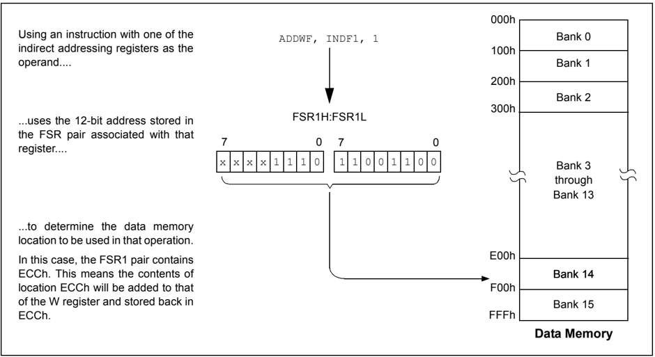
5.4.3.2 FSR Registers and POSTINC, POSTDEC, PREINC and PLUSW
In addition to the INDF operand, each FSR register pair also has four additional indirect operands. Like INDF, these are “virtual” registers that cannot be indirectly read or written to. Accessing these registers actually accesses the associated FSR register pair, but also performs a specific action on it stored value. They are:
- POSTDEC: accesses the FSR value, then automatically decrements it by ‘1’ afterwards
- POSTINC: accesses the FSR value, then automatically increments it by ‘1’ afterwards
- PREINC: increments the FSR value by ‘1’, then uses it in the operation
- PLUSW: adds the signed value of the W register (range of -127 to 128) to that of the FSR and uses the new value in the operation.
In this context, accessing an INDF register uses the value in the FSR registers without changing them. Similarly, accessing a PLUSW register gives the FSR value offset by that in the W register; neither value is actually changed in the operation. Accessing the other virtual registers changes the value of the FSR registers.
Operations on the FSRs with POSTDEC, POSTINC and PREINC affect the entire register pair; that is, rollovers of the FSRnL register, from FFh to 00h, carry over to the FSRnH register. On the other hand, results of these operations do not change the value of any flags in the STATUS register (e.g., Z, N, OV, etc.).
The PLUSW register can be used to implement a form of Indexed Addressing in the data memory space. By manipulating the value in the W register, users can reach addresses that are fixed offsets from pointer addresses. In some applications, this can be used to implement some powerful program control structure, such as software stacks, inside of data memory.
5.4.3.3 Operations by FSRs on FSRs
Indirect Addressing operations that target other FSRs or virtual registers represent special cases. For example, using an FSR to point to one of the virtual registers will not result in successful operations. As a specific case, assume that FSR0H:FSR0L contains FE7h, the address of INDF1. Attempts to read the value of INDF1, using INDF0 as an operand, will return 00h. Attempts to write to INDF1, using INDF0 as the operand, will result in a NOP.
On the other hand, using the virtual registers to write to an FSR pair may not occur as planned. In these cases, the value will be written to the FSR pair but without any incrementing or decrementing. Thus, writing to INDF2 or POSTDEC2 will write the same value to the FSR2H:FSR2L.
Since the FSRs are physical registers mapped in the SFR space, they can be manipulated through all direct operations. Users should proceed cautiously when working on these registers, particularly if their code uses Indirect Addressing.
Similarly, operations by Indirect Addressing are generally permitted on all other SFRs. Users should exercise the appropriate caution that they do not inadvertently change settings that might affect the operation of the device.
5.5 Program Memory and the Extended Instruction Set
The operation of program memory is unaffected by the use of the extended instruction set.
Enabling the extended instruction set adds eight additional two-word commands to the existing PIC18 instruction set: ADDFSR, ADDULNK, CALLW, MOVSF, MOVSS, PUSHL, SUBFSR and SUBULNK. These instructions are executed as described in Section 5.2.4 “Two-Word Instructions”.
5.6 Data Memory and the Extended Instruction Set
Enabling the PIC18 extended instruction set (XINST Configuration bit = 1) significantly changes certain aspects of data memory and its addressing. Specifically, the use of the Access Bank for many of the core PIC18 instructions is different. This is due to the introduction of a new addressing mode for the data memory space. This mode also alters the behavior of Indirect Addressing using FSR2 and its associated operands.
What does not change is just as important. The size of the data memory space is unchanged, as well as its linear addressing. The SFR map remains the same. Core PIC18 instructions can still operate in both Direct and Indirect Addressing mode; inherent and literal instructions do not change at all. Indirect Addressing with FSR0 and FSR1 also remains unchanged.
5.6.1 INDEXED ADDRESSING WITH LITERAL OFFSET
Enabling the PIC18 extended instruction set changes the behavior of Indirect Addressing using the FSR2 register pair and its associated file operands. Under the proper conditions, instructions that use the Access Bank – that is, most bit-oriented and byte-oriented instructions – can invoke a form of Indexed Addressing using an offset specified in the instruction. This special addressing mode is known as Indexed Addressing with Literal Offset or Indexed Literal Offset mode.
When using the extended instruction set, this addressing mode requires the following:
- The use of the Access Bank is forced (‘a’ = 0); and
- The file address argument is less than or equal to 5Fh.
Under these conditions, the file address of the instruction is not interpreted as the lower byte of an address (used with the BSR in Direct Addressing), or as an 8-bit address in the Access Bank. Instead, the value is interpreted as an offset value to an Address Pointer specified by FSR2. The offset and the contents of FSR2 are added to obtain the target address of the operation.
5.6.2 INSTRUCTIONS AFFECTED BY INDEXED LITERAL OFFSET MODE
Any of the core PIC18 instructions that can use Direct Addressing are potentially affected by the Indexed Literal Offset Addressing mode. This includes all byte-oriented and bit-oriented instructions, or almost one-half of the standard PIC18 instruction set. Instructions that only use Inherent or Literal Addressing modes are unaffected.
Additionally, byte-oriented and bit-oriented instructions are not affected if they do not use the Access Bank (Access RAM bit is ‘1’) or include a file address of 60h or above. Instructions meeting these criteria will continue to execute as before. A comparison of the different possible addressing modes when the extended instruction set is enabled in shown in Figure 5-8.
Those who desire to use byte-oriented or bit-oriented instructions in the Indexed Literal Offset mode should note the changes to assembler syntax for this mode. This is described in more detail in Section 26.2.1 “Extended Instruction Syntax”.
FIGURE 5-8: COMPARING ADDRESSING OPTIONS FOR BIT-ORIENTED AND BYTE-ORIENTED INSTRUCTIONS (EXTENDED INSTRUCTION SET ENABLED)
EXAMPLE INSTRUCTION: ADDWF, f, d, a (Opcode: 0010 01da ffff ffff)
When a = 0 and f ≥ 60h: The instruction executes in Direct Forced mode. ‘f’ is interpreted as a location in the Access RAM between 060h and 0FFh. This is the same as the SFRs or locations F60h to 0FFh (Bank 15) of data memory. Locations below 60h are not available in this addressing mode.
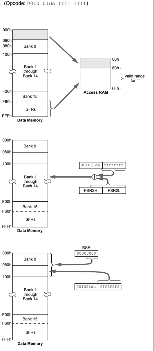
When a = 0 and f ≤ 5Fh: The instruction executes in Indexed Literal Offset mode. ‘f’ is interpreted as an offset to the address value in FSR2. The two are added together to obtain the address of the target register for the instruction. The address can be anywhere in the data memory space. Note that in this mode, the correct syntax is now: ADDWF [k], d where ‘k’ is the same as ‘f’.
When a = 1 (all values of f): The instruction executes in Direct mode (also known as Direct Long mode). ‘f’ is interpreted as a location in one of the 16 banks of the data memory space. The bank is designated by the Bank Select Register (BSR). The address can be in any implemented bank in the data memory space.
DS39632E-page 78 © 2009 Microchip Technology Inc.
5.6.3 MAPPING THE ACCESS BANK IN INDEXED LITERAL OFFSET MODE
The use of Indexed Literal Offset Addressing mode effectively changes how the lower portion of Access RAM (00h to 5Fh) is mapped. Rather than containing just the contents of the bottom half of Bank 0, this mode maps the contents from Bank 0 and a user-defined "window" that can be located anywhere in the data memory space. The value of FSR2 establishes the lower boundary of the addresses mapped into the window, while the upper boundary is defined by FSR2 plus 95 (5Fh). Addresses in the Access RAM above 5Fh are mapped as previously described (see Section 5.3.3 "Access Bank"). An example of Access Bank remapping in this addressing mode is shown in Figure 5-9.
Remapping of the Access Bank applies only to operations using the Indexed Literal Offset mode. Operations that use the BSR (Access RAM bit is '1') will continue to use Direct Addressing as before. Any indirect or indexed operation that explicitly uses any of the indirect file operands (including FSR2) will continue to operate as standard Indirect Addressing. Any instruction that uses the Access Bank, but includes a register address of greater than 05Fh, will use Direct Addressing and the normal Access Bank map.
5.6.4 BSR IN INDEXED LITERAL OFFSET MODE
Although the Access Bank is remapped when the extended instruction set is enabled, the operation of the BSR remains unchanged. Direct Addressing, using the BSR to select the data memory bank, operates in the same manner as previously described.
FIGURE 5-9: REMAPPING THE ACCESS BANK WITH INDEXED LITERAL OFFSET ADDRESSING