29.0 DC AND AC CHARACTERISTICS GRAPHS AND TABLES
Graphs and tables are not available at this time.
NOTES:
30.0 PACKAGING INFORMATION
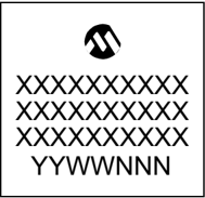
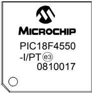
30.1 Package Marking Information
28-Lead PDIP (Skinny DIP)
 Example
PIC18F2455-I/SP e3
0810017
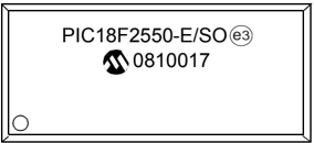
28-Lead SOIC
 Example
PIC18F2550-E/SO e3
0810017
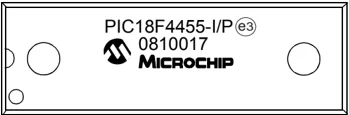
40-Lead PDIP
 Example
PIC18F4455-I/P e3
0810017
MICROCHIP
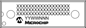
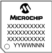
Legend: XX...X Customer-specific information Y Year code (last digit of calendar year) YY Year code (last 2 digits of calendar year) WW Week code (week of January 1 is week '01') NNN Alphanumeric traceability code e3 Pb-free JEDEC designator for Matte Tin (Sn)
- This package is Pb-free. The Pb-free JEDEC designator (e3) can be found on the outer packaging for this package.
Note: In the event the full Microchip part number cannot be marked on one line, it will be carried over to the next line, thus limiting the number of available characters for customer-specific information.
Package Marking Information (Continued)
44-Lead TQFP
Example
44-Lead QFN
Example
30.2 Package Details
The following sections give the technical details of the packages.
28-Lead Skinny Plastic Dual In-Line (SP) – 300 mil Body [SPDIP]
Note: For the most current package drawings, please see the Microchip Packaging Specification located at http://www.microchip.com/packaging
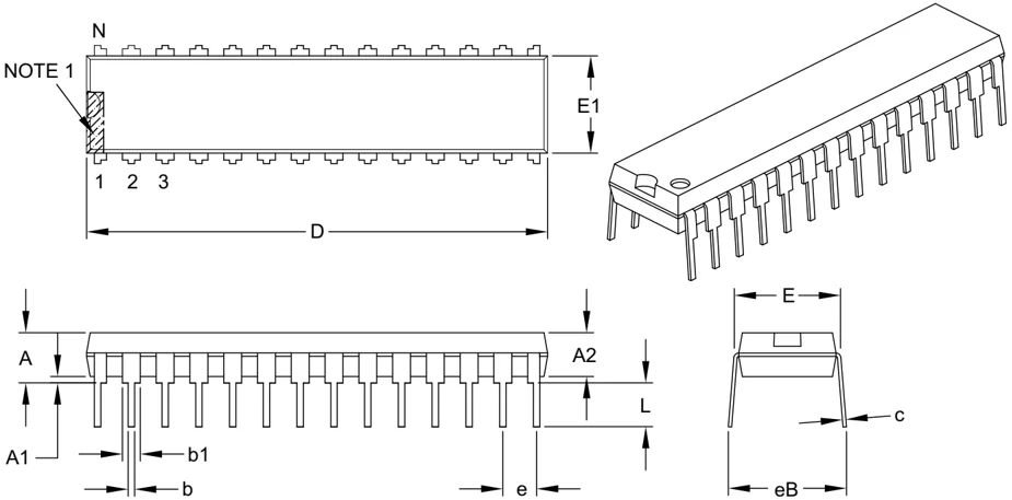
Units INCHES Dimension Limits MIN NOM MAX Number of Pins N 28 Pitch e .100 BSC Top to Seating Plane A – – .200 Molded Package Thickness A2 .120 .135 .150 Base to Seating Plane A1 .015 – – Shoulder to Shoulder Width E .290 .310 .335 Molded Package Width E1 .240 .285 .295 Overall Length D 1.345 1.365 1.400 Tip to Seating Plane L .110 .130 .150 Lead Thickness c .008 .010 .015 Upper Lead Width b1 .040 .050 .070 Lower Lead Width b .014 .018 .022 Overall Row Spacing § eB – – .430
Notes:
- Pin 1 visual index feature may vary, but must be located within the hatched area.
- § Significant Characteristic.
- Dimensions D and E1 do not include mold flash or protrusions. Mold flash or protrusions shall not exceed .010" per side.
- Dimensioning and tolerancing per ASME Y14.5M. BSC: Basic Dimension. Theoretically exact value shown without tolerances.
Microchip Technology Drawing C04-070B
28-Lead Plastic Small Outline (SO) – Wide, 7.50 mm Body [SOIC]
Note: For the most current package drawings, please see the Microchip Packaging Specification located at http://www.microchip.com/packaging
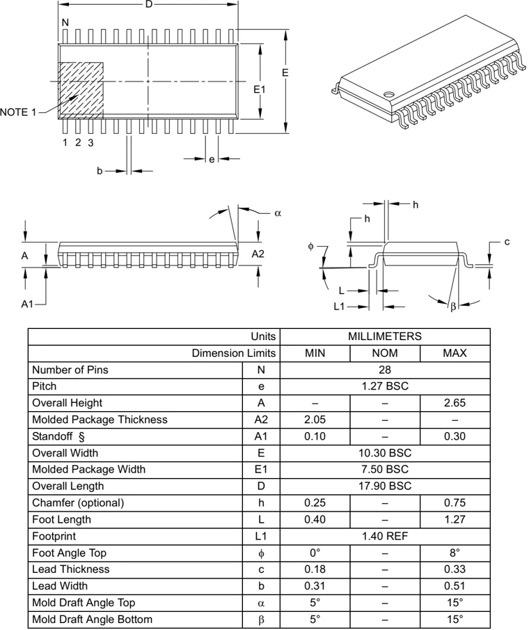
| Units | MILLIMETERS | |||
|---|---|---|---|---|
| Dimension Limits | MIN | NOM | MAX | |
| Number of Pins | N | 28 | ||
| Pitch | e | 1.27 BSC | ||
| Overall Height | A | – | – | 2.65 |
| Molded Package Thickness | A2 | 2.05 | – | – |
| Standoff § | A1 | 0.10 | – | 0.30 |
| Overall Width | E | 10.30 BSC | ||
| Molded Package Width | E1 | 7.50 BSC | ||
| Overall Length | D | 17.90 BSC | ||
| Chamfer (optional) | h | 0.25 | – | 0.75 |
| Foot Length | L | 0.40 | – | 1.27 |
| Footprint | L1 | 1.40 REF | ||
| Foot Angle Top | φ | 0° | – | 8° |
| Lead Thickness | c | 0.18 | – | 0.33 |
| Lead Width | b | 0.31 | – | 0.51 |
| Mold Draft Angle Top | α | 5° | – | 15° |
| Mold Draft Angle Bottom | β | 5° | – | 15° |
Notes:
- Pin 1 visual index feature may vary, but must be located within the hatched area.
- § Significant Characteristic.
- Dimensions D and E1 do not include mold flash or protrusions. Mold flash or protrusions shall not exceed 0.15 mm per side.
- Dimensioning and tolerancing per ASME Y14.5M.
- BSC: Basic Dimension. Theoretically exact value shown without tolerances.
- REF: Reference Dimension, usually without tolerance, for information purposes only.
Microchip Technology Drawing C04-052B
40-Lead Plastic Dual In-Line (P) – 600 mil Body [PDIP]
Note: For the most current package drawings, please see the Microchip Packaging Specification located at http://www.microchip.com/packaging
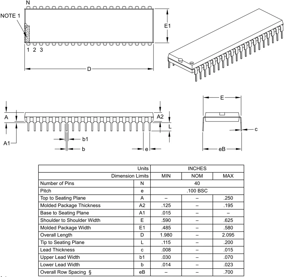
\begin{tabular}{|l|c|c|c|c|} \hline \multicolumn{2}{|c|}{} & Units & \multicolumn{3}{c|}{INCHES} \ \cline{3-5} \multicolumn{2}{|c|}{Dimension Limits} & & MIN & NOM & MAX \ \hline Number of Pins & N & \multicolumn{3}{c|}{40} \ \hline Pitch & e & \multicolumn{3}{c|}{.100 BSC} \ \hline Top to Seating Plane & A & -- & -- & .250 \ \hline Molded Package Thickness & A2 & .125 & -- & .195 \ \hline Base to Seating Plane & A1 & .015 & -- & -- \ \hline Shoulder to Shoulder Width & E & .590 & -- & .625 \ \hline Molded Package Width & E1 & .485 & -- & .580 \ \hline Overall Length & D & 1.980 & -- & 2.095 \ \hline Tip to Seating Plane & L & .115 & -- & .200 \ \hline Lead Thickness & c & .008 & -- & .015 \ \hline Upper Lead Width & b1 & .030 & -- & .070 \ \hline Lower Lead Width & b & .014 & -- & .023 \ \hline Overall Row Spacing § & eB & -- & -- & .700 \ \hline \end{tabular}
Notes:
- Pin 1 visual index feature may vary, but must be located within the hatched area.
- § Significant Characteristic.
- Dimensions D and E1 do not include mold flash or protrusions. Mold flash or protrusions shall not exceed .010" per side.
- Dimensioning and tolerancing per ASME Y14.5M. BSC: Basic Dimension. Theoretically exact value shown without tolerances.
Microchip Technology Drawing C04-016B
44-Lead Plastic Thin Quad Flatpack (PT) – 10x10x1 mm Body, 2.00 mm [TQFP]
Note: For the most current package drawings, please see the Microchip Packaging Specification located at http://www.microchip.com/packaging
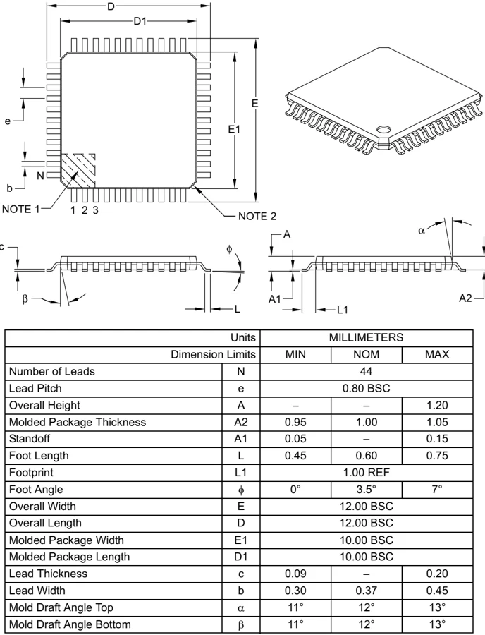
| Units | MILLIMETERS | |||
|---|---|---|---|---|
| Dimension Limits | MIN | NOM | MAX | |
| Number of Leads | N | 44 | ||
| Lead Pitch | e | 0.80 BSC | ||
| Overall Height | A | – | – | 1.20 |
| Molded Package Thickness | A2 | 0.95 | 1.00 | 1.05 |
| Standoff | A1 | 0.05 | – | 0.15 |
| Foot Length | L | 0.45 | 0.60 | 0.75 |
| Footprint | L1 | 1.00 REF | ||
| Foot Angle | φ | 0° | 3.5° | 7° |
| Overall Width | E | 12.00 BSC | ||
| Overall Length | D | 12.00 BSC | ||
| Molded Package Width | E1 | 10.00 BSC | ||
| Molded Package Length | D1 | 10.00 BSC | ||
| Lead Thickness | c | 0.09 | – | 0.20 |
| Lead Width | b | 0.30 | 0.37 | 0.45 |
| Mold Draft Angle Top | α | 11° | 12° | 13° |
| Mold Draft Angle Bottom | β | 11° | 12° | 13° |
Notes:
- Pin 1 visual index feature may vary, but must be located within the hatched area.
- Chamfers at corners are optional; size may vary.
- Dimensions D1 and E1 do not include mold flash or protrusions. Mold flash or protrusions shall not exceed 0.25 mm per side.
- Dimensioning and tolerancing per ASME Y14.5M.
BSC: Basic Dimension. Theoretically exact value shown without tolerances.
REF: Reference Dimension, usually without tolerance, for information purposes only.
Microchip Technology Drawing C04-076B
44-Lead Plastic Thin Quad Flatpack (PT) – 10x10x1 mm Body, 2.00 mm [TQFP]
Note: For the most current package drawings, please see the Microchip Packaging Specification located at http://www.microchip.com/packaging
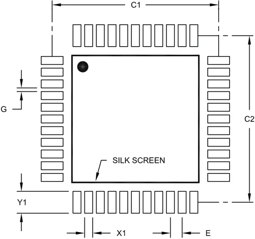
RECOMMENDED LAND PATTERN
| Units | MILLIMETERS | |||
|---|---|---|---|---|
| Dimension Limits | MIN | NOM | MAX | |
| Contact Pitch | E | 0.80 BSC | ||
| Contact Pad Spacing | C1 | 11.40 | ||
| Contact Pad Spacing | C2 | 11.40 | ||
| Contact Pad Width (X44) | X1 | 0.55 | ||
| Contact Pad Length (X44) | Y1 | 1.50 | ||
| Distance Between Pads | G | 0.25 |
Notes:
- Dimensioning and tolerancing per ASME Y14.5M
BSC: Basic Dimension. Theoretically exact value shown without tolerances.
Microchip Technology Drawing No. C04-2076A
44-Lead Plastic Quad Flat, No Lead Package (ML) – 8x8 mm Body [QFN]
Note: For the most current package drawings, please see the Microchip Packaging Specification located at http://www.microchip.com/packaging
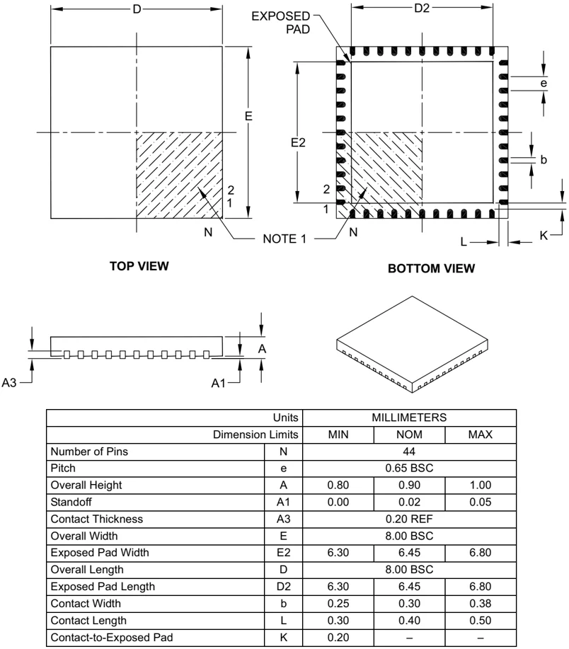
| Units | MILLIMETERS | |||
|---|---|---|---|---|
| Dimension Limits | MIN | NOM | MAX | |
| Number of Pins | N | 44 | ||
| Pitch | e | 0.65 BSC | ||
| Overall Height | A | 0.80 | 0.90 | 1.00 |
| Standoff | A1 | 0.00 | 0.02 | 0.05 |
| Contact Thickness | A3 | 0.20 REF | ||
| Overall Width | E | 8.00 BSC | ||
| Exposed Pad Width | E2 | 6.30 | 6.45 | 6.80 |
| Overall Length | D | 8.00 BSC | ||
| Exposed Pad Length | D2 | 6.30 | 6.45 | 6.80 |
| Contact Width | b | 0.25 | 0.30 | 0.38 |
| Contact Length | L | 0.30 | 0.40 | 0.50 |
| Contact-to-Exposed Pad | K | 0.20 | – | – |
Notes:
- Pin 1 visual index feature may vary, but must be located within the hatched area.
- Package is saw singulated.
- Dimensioning and tolerancing per ASME Y14.5M.
BSC: Basic Dimension. Theoretically exact value shown without tolerances.
REF: Reference Dimension, usually without tolerance, for information purposes only.
Microchip Technology Drawing C04-103B
DS39632E-page 416 © 2009 Microchip Technology Inc.
44-Lead Plastic Quad Flat, No Lead Package (ML) – 8x8 mm Body [QFN]
Note: For the most current package drawings, please see the Microchip Packaging Specification located at http://www.microchip.com/packaging
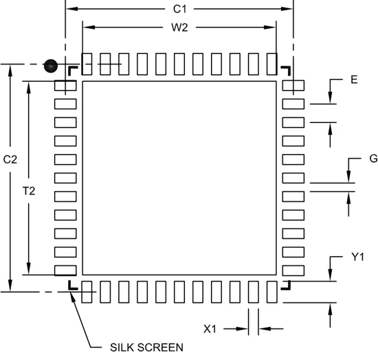
RECOMMENDED LAND PATTERN
| Units | MILLIMETERS | |||
|---|---|---|---|---|
| Dimension Limits | MIN | NOM | MAX | |
| Contact Pitch | E | 0.65 BSC | ||
| Optional Center Pad Width | W2 | 6.80 | ||
| Optional Center Pad Length | T2 | 6.80 | ||
| Contact Pad Spacing | C1 | 8.00 | ||
| Contact Pad Spacing | C2 | 8.00 | ||
| Contact Pad Width (X44) | X1 | 0.35 | ||
| Contact Pad Length (X44) | Y1 | 0.80 | ||
| Distance Between Pads | G | 0.25 |
Notes:
- Dimensioning and tolerancing per ASME Y14.5M
BSC: Basic Dimension. Theoretically exact value shown without tolerances.
Microchip Technology Drawing No. C04-2103A
NOTES:
APPENDIX A: REVISION HISTORY
Revision A (May 2004)
Original data sheet for PIC18F2455/2550/4455/4550 devices.
Revision B (October 2004)
This revision includes updates to the Electrical Specifications in Section 28.0 “Electrical Characteristics” and includes minor corrections to the data sheet text.
Revision C (February 2006)
This revision includes updates to Section 19.0 “Master Synchronous Serial Port (MSSP) Module”, Section 20.0 “Enhanced Universal Synchronous Asynchronous Receiver Transmitter (EUSART)” and the Electrical Specifications in Section 28.0 “Electrical Characteristics” and includes minor corrections to the data sheet text.
Revision D (January 2007)
This revision includes updates to the packaging diagrams.
Revision E (August 2008)
This revision includes minor corrections to the data sheet text. In Section 30.2 “Package Details”, added land pattern drawings for both 44-pin packages.
APPENDIX B: DEVICE DIFFERENCES
The differences between the devices listed in this data sheet are shown in Table B-1.
TABLE B-1: DEVICE DIFFERENCES
| Features | PIC18F2455 | PIC18F2550 | PIC18F4455 | PIC18F4550 |
|---|---|---|---|---|
| Program Memory (Bytes) | 24576 | 32768 | 24576 | 32768 |
| Program Memory (Instructions) | 12288 | 16384 | 12288 | 16384 |
| Interrupt Sources | 19 | 19 | 20 | 20 |
| I/O Ports | Ports A, B, C, (E) | Ports A, B, C, (E) | Ports A, B, C, D, E | Ports A, B, C, D, E |
| Capture/Compare/PWM Modules | 2 | 2 | 1 | 1 |
| Enhanced Capture/Compare/PWM Modules | 0 | 0 | 1 | 1 |
| Parallel Communications (SPP) | No | No | Yes | Yes |
| 10-Bit Analog-to-Digital Module | 10 Input Channels | 10 Input Channels | 13 Input Channels | 13 Input Channels |
| Packages | 28-Pin PDIP28-Pin SOIC | 28-Pin PDIP28-Pin SOIC | 40-Pin PDIP44-Pin TQFP44-Pin QFN | 40-Pin PDIP44-Pin TQFP44-Pin QFN |
APPENDIX C: CONVERSION CONSIDERATIONS
This appendix discusses the considerations for converting from previous versions of a device to the ones listed in this data sheet. Typically, these changes are due to the differences in the process technology used. An example of this type of conversion is from a PIC16C74A to a PIC16C74B.
Not Applicable
APPENDIX D: MIGRATION FROM BASELINE TO ENHANCED DEVICES
This section discusses how to migrate from a Baseline device (i.e., PIC16C5X) to an Enhanced MCU device (i.e., PIC18FXXX).
The following are the list of modifications over the PIC16C5X microcontroller family:
Not Currently Available
DS39632E-page 420 © 2009 Microchip Technology Inc.
APPENDIX E: MIGRATION FROM MID-RANGE TO ENHANCED DEVICES
A detailed discussion of the differences between the mid-range MCU devices (i.e., PIC16CXXX) and the enhanced devices (i.e., PIC18FXXX) is provided in AN716, "Migrating Designs from PIC16C74A/74B to PIC18C442". The changes discussed, while device specific, are generally applicable to all mid-range to enhanced device migrations.
This Application Note is available as Literature Number DS00716.
APPENDIX F: MIGRATION FROM HIGH-END TO ENHANCED DEVICES
A detailed discussion of the migration pathway and differences between the high-end MCU devices (i.e., PIC17CXXX) and the enhanced devices (i.e., PIC18FXXX) is provided in AN726, "PIC17CXXX to PIC18CXXX Migration". This Application Note is available as Literature Number DS00726.
NOTES:
INDEX
A
- A/D ........ 265
- Acquisition Requirements ........ 270
- ADCON0 Register ........ 265
- ADCON1 Register ........ 265
- ADCON2 Register ........ 265
- ADRESH Register ........ 265, 268
- ADRESL Register ........ 265
- Analog Port Pins, Configuring ........ 272
- Associated Registers ........ 274
- Configuring the Module ........ 269
- Conversion Clock (TAD) ........ 271
- Conversion Requirements ........ 405
- Conversion Status (GO/DONE Bit) ........ 268
- Conversions ........ 273
- Converter Characteristics ........ 404
- Converter Interrupt, Configuring ........ 269
- Discharge ........ 273
- Operation in Power-Managed Modes ........ 272
- Selecting and Configuring Acquisition Time ........ 271
- Special Event Trigger (CCP2) ........ 274
- Special Event Trigger (ECCP) ........ 152
- Use of the CCP2 Trigger ........ 274
- Absolute Maximum Ratings ........ 367
- AC (Timing) Characteristics ........ 385 Load Conditions for Device Timing
- Specifications ........ 386
- Parameter Symbology ........ 385
- Temperature and Voltage Specifications ........ 386
- Timing Conditions ........ 386 AC Characteristics
- Internal RC Accuracy ........ 388 Access Bank
- Mapping with Indexed Literal Offset Mode ........ 79
- ACKSTAT ........ 232
- ACKSTAT Status Flag ........ 232
- ADCON0 Register ........ 265
- GO/DONE Bit ........ 268
- ADCON1 Register ........ 265
- ADCON2 Register ........ 265
- ADDFSR ........ 356
- ADDLW ........ 319
- ADDULNK ........ 356
- ADDWF ........ 319
- ADDWFC ........ 320
- ADRESH Register ........ 265
- ADRESL Register ........ 265, 268 Analog-to-Digital Converter. See A/D.
- and BSR ........ 79
- ANDLW ........ 320
- ANDWF ........ 321 Assembler
- MPASM Assembler ........ 364
B
- Baud Rate Generator ........ 228
- BC ........ 321
- BCF ........ 322
- BF ........ 232
- BF Status Flag ........ 232
Block Diagrams
- A/D ........ 268
- Analog Input Model ........ 269
- Baud Rate Generator ........ 228
- Capture Mode Operation ........ 145
- Comparator Analog Input Model ........ 279
- Comparator I/O Operating Modes ........ 276
- Comparator Output ........ 278
- Comparator Voltage Reference ........ 282 Comparator Voltage Reference
- Output Buffer Example ........ 283
- Compare Mode Operation ........ 146
- Device Clock ........ 24
- Enhanced PWM ........ 153
- EUSART Receive ........ 257
- EUSART Transmit ........ 254 External Power-on Reset Circuit
- (Slow VDD Power-up) ........ 47
- Fail-Safe Clock Monitor ........ 306
- Generic I/O Port ........ 113
- High/Low-Voltage Detect with External Input ........ 286
- Interrupt Logic ........ 100
- MSSP (I²C Master Mode) ........ 226
- MSSP (I²C Mode) ........ 207
- MSSP (SPI Mode) ........ 197
- On-Chip Reset Circuit ........ 45
- PIC18F2455/2550 ........ 10
- PIC18F4455/4550 ........ 11
- PLL (HS Mode) ........ 27
- PWM Operation (Simplified) ........ 148
- Reads from Flash Program Memory ........ 85
- Single Comparator ........ 277
- SPP Data Path ........ 191
- Table Read Operation ........ 81
- Table Write Operation ........ 82
- Table Writes to Flash Program Memory ........ 87
- Timer0 in 16-Bit Mode ........ 128
- Timer0 in 8-Bit Mode ........ 128
- Timer1 ........ 132
- Timer1 (16-Bit Read/Write Mode) ........ 132
- Timer2 ........ 138
- Timer3 ........ 140
- Timer3 (16-Bit Read/Write Mode) ........ 140
- USB Interrupt Logic ........ 180
- USB Peripheral and Options ........ 165
- Watchdog Timer ........ 303
- BN ........ 322
- BNC ........ 323
- BNN ........ 323
- BNOV ........ 324
- BNZ ........ 324 BOR. See Brown-out Reset.
- BOV ........ 327
- BRA ........ 325
- Break Character (12-Bit) Transmit and Receive ........ 259 BRG. See Baud Rate Generator.
- Brown-out Reset (BOR) ........ 48
- Detecting ........ 48
- Disabling in Sleep Mode ........ 48
- Software Enabled ........ 48
- BSF ........ 325
- BTFSC ........ 326
- BTFSS ........ 326
- BTG ........ 327
- BZ ........ 328
C C Compilers
- MPLAB C18 ........ 364
- MPLAB C30 ........ 364
- CALL ........ 328
- CALLW ........ 357
- Capture (CCP Module) ........ 145
- CCP Pin Configuration ........ 145
- CCPRxH:CCPRxL Registers ........ 145
- Prescaler ........ 145
- Software Interrupt ........ 145
- Timer1/Timer3 Mode Selection ........ 145
- Capture (ECCP Module) ........ 152 Capture/Compare (CCP Module)
- Associated Registers ........ 147
- Capture/Compare/PWM (CCP) ........ 143 Capture Mode. See Capture.
- CCP Mode and Timer Resources ........ 144
- CCP2 Pin Assignment ........ 144
- CCPRxH Register ........ 144
- CCPRxL Register ........ 144 Compare Mode. See Compare. Interaction of Two CCP Modules for
- Timer Resources ........ 144
- Module Configuration ........ 144
- Clock Sources ........ 32
- Effects of Power-Managed Modes ........ 34
- Selecting the 31 kHz Source ........ 32
- Selection Using OSCCON Register ........ 32
- CLRF ........ 329
- CLRWDT ........ 329 Code Examples
- 16 x 16 Signed Multiply Routine ........ 98
- 16 x 16 Unsigned Multiply Routine ........ 98
- 8 x 8 Signed Multiply Routine ........ 97
- 8 x 8 Unsigned Multiply Routine ........ 97
- Changing Between Capture Prescalers ........ 145
- Computed GOTO Using an Offset Value ........ 62
- Data EEPROM Read ........ 93
- Data EEPROM Refresh Routine ........ 94
- Data EEPROM Write ........ 93
- Erasing a Flash Program Memory Row ........ 86 Executing Back to Back SLEEP Instructions ... 36
- Fast Register Stack ........ 62 How to Clear RAM (Bank 1) Using
- Indirect Addressing ........ 74 Implementing a Real-Time Clock Using
- a Timer1 Interrupt Service ........ 135
- Initializing PORTA ........ 113
- Initializing PORTB ........ 116
- Initializing PORTC ........ 119
- Initializing PORTD ........ 122
- Initializing PORTE ........ 125
- Loading the SSPBUF (SSPSR) Register ........ 200
- Reading a Flash Program Memory Word ........ 85 Saving STATUS, WREG and BSR
- Registers in RAM ........ 111
- Writing to Flash Program Memory ........ 88–89
- Code Protection ........ 291
- COMF ........ 330
- Comparator ........ 275
- Analog Input Connection Considerations ........ 279
- Associated Registers ........ 279
- Configuration ........ 276
- Effects of a Reset ........ 278
- Interrupts ........ 278
- Operation ........ 277
- Operation During Sleep ........ 278
- Outputs ........ 277
- Reference ........ 277
- External Signal ........ 277
- Internal Signal ........ 277
- Response Time ........ 277
- Comparator Specifications ........ 382
- Comparator Voltage Reference ........ 281
- Accuracy and Error ........ 282
- Associated Registers ........ 283
- Configuring ........ 281
- Connection Considerations ........ 282
- Effects of a Reset ........ 282
- Operation During Sleep ........ 282
- Compare (CCP Module) ........ 146
- CCP Pin Configuration ........ 146
- CCPRx Register ........ 146
- Software Interrupt ........ 146
- Special Event Trigger ........ 141, 146, 274
- Timer1/Timer3 Mode Selection ........ 146
- Compare (ECCP Module) ........ 152
- Special Event Trigger ........ 152
- Configuration Bits ........ 292
- Configuration Register Protection ........ 311
- Context Saving During Interrupts ........ 111
- Conversion Considerations ........ 420
- CPFSEQ ........ 330
- CPFSGT ........ 331
- CPFSLT ........ 331
- Crystal Oscillator/Ceramic Resonator ........ 25
- Customer Change Notification Service ........ 433
- Customer Notification Service ........ 433
- Customer Support ........ 433
D
- Data Addressing Modes ........ 74 Comparing Addressing Modes with the
- Extended Instruction Set Enabled ........ 78
- Direct ........ 74
- Indexed Literal Offset ........ 77
- Indirect ........ 74
- Inherent and Literal ........ 74 Data EEPROM
- Code Protection ........ 311
- Data EEPROM Memory ........ 91
- Associated Registers ........ 95
- EECON1 and EECON2 Registers ........ 91
- Operation During Code-Protect ........ 94
- Protection Against Spurious Write ........ 94
- Reading ........ 93
- Using ........ 94
- Write Verify ........ 93
- Writing ........ 93
- Data Memory ........ 65
- Access Bank ........ 67
- and the Extended Instruction Set ........ 77
- Bank Select Register (BSR) ........ 65
- General Purpose Registers ........ 67 Map for PIC18F2455/2550/4455/4550 Devices 66
- Special Function Registers ........ 68
- Map ........ 68
- USB RAM ........ 65
- DAW ........ 332
DS39632E-page 424 © 2009 Microchip Technology Inc.
DC and AC Characteristics
- Graphs and Tables ........ 407
- DC Characteristics ........ 379
- Power-Down and Supply Current ........ 370
- Supply Voltage ........ 369
- DCFSNZ ........ 333
- DECF ........ 332
- DECFSZ ........ 333
- Dedicated ICD/ICSP Port ........ 311
- Development Support ........ 363
- Device Differences ........ 419
- Device Overview ........ 7
- Features (table) ........ 9
- New Core Features ........ 7
- Other Special Features ........ 8
- Device Reset Timers ........ 49
- Oscillator Start-up Timer (OST) ........ 49
- PLL Lock Time-out ........ 49
- Power-up Timer (PWRT) ........ 49
- Direct Addressing ........ 75
E
- Effect on Standard PIC MCU Instructions ........ 77, 360
- Electrical Characteristics ........ 367
- Enhanced Capture/Compare/PWM (ECCP) ........ 151
- Associated Registers ........ 164
- Capture and Compare Modes ........ 152 Capture Mode. See Capture (ECCP Module).
- Outputs and Configuration ........ 152
- Pin Configurations for ECCP1 ........ 152 PWM Mode. See PWM (ECCP Module).
- Standard PWM Mode ........ 152
- Timer Resources ........ 152 Enhanced Universal Synchronous Asynchronous Receiver Transmitter (EUSART). See EUSART. Equations
- A/D Acquisition Time ........ 270
- A/D Minimum Charging Time ........ 270 Calculating the Minimum Required A/D
- Acquisition Time ........ 270
- Errata ........ 5 EUSART
- Asynchronous Mode ........ 253
- 12-Bit Break Transmit and Receive ........ 259
- Associated Registers, Receive ........ 257
- Associated Registers, Transmit ........ 255
- Auto-Wake-up on Sync Break Character ........ 258
- Receiver ........ 256 Setting up 9-Bit Mode with
- Address Detect ........ 256
- Transmitter ........ 253 Baud Rate Generator
- Operation in Power-Managed Modes ........ 247
- Baud Rate Generator (BRG) ........ 247
- Associated Registers ........ 248
- Auto-Baud Rate Detect ........ 251
- Baud Rate Error, Calculating ........ 248
- Baud Rates, Asynchronous Modes ........ 249
- High Baud Rate Select (BRGH Bit) ........ 247
- Sampling ........ 247
- Synchronous Master Mode ........ 260
- Associated Registers, Receive ........ 262
- Associated Registers, Transmit ........ 261
- Reception ........ 262
- Transmission ........ 260
- Synchronous Slave Mode ........ 263
- Associated Registers, Receive ........ 264
- Associated Registers, Transmit ........ 263
- Reception ........ 264
- Transmission ........ 263
- Extended Instruction Set ........ 355
- ADDFSR ........ 356
- ADDULNK ........ 356
- and Using MPLAB IDE Tools ........ 362
- CALLW ........ 357
- Considerations for Use ........ 360
- MOVSF ........ 357
- MOVSS ........ 358
- PUSHL ........ 358
- SUBFSR ........ 359
- SUBULNK ........ 359
- Syntax ........ 355
- External Clock Input ........ 26
F
- Fail-Safe Clock Monitor ........ 291, 306
- Exiting the Operation ........ 306
- Interrupts in Power-Managed Modes ........ 307
- POR or Wake-up from Sleep ........ 307
- WDT During Oscillator Failure ........ 306
- Fast Register Stack ........ 62
- Firmware Instructions ........ 313
- Flash Program Memory ........ 81
- Associated Registers ........ 89
- Control Registers ........ 82
- EECON1 and EECON2 ........ 82
- TABLAT (Table Latch) Register ........ 84
- TBLPTR (Table Pointer) Register ........ 84
- Erase Sequence ........ 86
- Erasing ........ 86
- Operation During Code-Protect ........ 89
- Protection Against Spurious Writes ........ 89
- Reading ........ 85 Table Pointer
- Boundaries Based on Operation ........ 84
- Table Pointer Boundaries ........ 84
- Table Reads and Table Writes ........ 81
- Unexpected Termination of Write ........ 89
- Write Sequence ........ 87
- Write Verify ........ 89
- Writing To ........ 87 FSCM. See Fail-Safe Clock Monitor.
G
- GOTO ........ 334
H
- Hardware Multiplier ........ 97
- Introduction ........ 97
- Operation ........ 97
- Performance Comparison ........ 97
- High/Low-Voltage Detect ........ 285
- Applications ........ 288
- Associated Registers ........ 289
- Characteristics ........ 384
- Current Consumption ........ 287
- Effects of a Reset ........ 289
- Operation ........ 286
- During Sleep ........ 289
- Setup ........ 287
- Start-up Time ........ 287
- Typical Application ........ 288
- HLVD. See High/Low-Voltage Detect. ........ 285
I
-
I/O Ports ........ 113 I²C Mode (MSSP)
-
Acknowledge Sequence Timing ........ 235
-
Associated Registers ........ 241
-
Baud Rate Generator ........ 228 Bus Collision
-
During a Repeated Start Condition ........ 239
-
During a Stop Condition ........ 240
-
Clock Arbitration ........ 229
-
Clock Stretching ........ 221
-
10-Bit Slave Receive Mode (SEN = 1) ........ 221
-
10-Bit Slave Transmit Mode ........ 221
-
7-Bit Slave Receive Mode (SEN = 1) ........ 221
-
7-Bit Slave Transmit Mode ........ 221
-
Clock Synchronization and the CKP Bit ........ 222
-
Effect of a Reset ........ 236
-
General Call Address Support ........ 225
-
I²C Clock Rate w/BRG ........ 228
-
Master Mode ........ 226
-
Operation ........ 227
-
Reception ........ 232
-
Repeated Start Condition Timing ........ 231
-
Start Condition Timing ........ 230
-
Transmission ........ 232
-
Transmit Sequence ........ 227 Multi-Master Communication, Bus Collision
-
and Arbitration ........ 236
-
Multi-Master Mode ........ 236
-
Operation ........ 212
-
Read/Write Bit Information (R/W̅ Bit) ........ 212, 214
-
Registers ........ 207
-
Serial Clock (RB1/AN10/INT1/SCK/SCL) ........ 214
-
Slave Mode ........ 212
-
Addressing ........ 212
-
Addressing Masking ........ 213
-
Reception ........ 214
-
Transmission ........ 214
-
Sleep Operation ........ 236
-
Stop Condition Timing ........ 235
-
ID Locations ........ 291, 311
-
Idle Modes ........ 40
-
INCF ........ 334
-
INCFSZ ........ 335
-
In-Circuit Debugger ........ 311
-
In-Circuit Serial Programming (ICSP) ........ 291, 311 Indexed Literal Offset Addressing
-
and Standard PIC18 Instructions ........ 360
-
Indexed Literal Offset Mode ........ 77, 79, 360
-
Indirect Addressing ........ 75
-
INFSNZ ........ 335
-
Initialization Conditions for all Registers ........ 53–57
-
Instruction Cycle ........ 63
-
Clocking Scheme ........ 63
-
Flow/Pipelining ........ 63
-
Instruction Set ........ 313
-
ADDLW ........ 319
-
ADDWF ........ 319
-
ADDWF (Indexed Literal Offset mode) ........ 361
-
ADDWFC ........ 320
-
ANDLW ........ 320
-
ANDWF ........ 321
-
BC ........ 321
-
BCF ........ 322
-
BN ........ 322
-
BNC ........ 323
-
BNN ........ 323
-
BNOV ........ 324
-
BNZ ........ 324
-
BOV ........ 327
-
BRA ........ 325
-
BSF ........ 325
-
BSF (Indexed Literal Offset mode) ........ 361
-
BTFSC ........ 326
-
BTFSS ........ 326
-
BTG ........ 327
-
BZ ........ 328
-
CALL ........ 328
-
CLRF ........ 329
-
CLRWDT ........ 329
-
COMF ........ 330
-
CPFSEQ ........ 330
-
CPFSGT ........ 331
-
CPFSLT ........ 331
-
DAW ........ 332
-
DCFSNZ ........ 333
-
DECF ........ 332
-
DECFSZ ........ 333
-
General Format ........ 315
-
GOTO ........ 334
-
INCF ........ 334
-
INCFSZ ........ 335
-
INFSNZ ........ 335
-
IORLW ........ 336
-
IORWF ........ 336
-
LFSR ........ 337
-
MOVF ........ 337
-
MOVFF ........ 338
-
MOVLB ........ 338
-
MOVLW ........ 339
-
MOVWF ........ 339
-
MULLW ........ 340
-
MULWF ........ 340
-
NEGF ........ 341
-
NOP ........ 341
-
Opcode Field Descriptions ........ 314
-
POP ........ 342
-
PUSH ........ 342
-
RCALL ........ 343
-
RESET ........ 343
-
RETFIE ........ 344
-
RETLW ........ 344
-
RETURN ........ 345
-
RLCF ........ 345
-
RLNCF ........ 346
-
RRCF ........ 346
-
RRNCF ........ 347
DS39632E-page 426 © 2009 Microchip Technology Inc.
- SETF ........ 347
- SETF (Indexed Literal Offset mode) ........ 361
- SLEEP ........ 348
- Standard Instructions ........ 313
- SUBFWB ........ 348
- SUBLW ........ 349
- SUBWF ........ 349
- SUBWFB ........ 350
- SWAPF ........ 350
- TBLRD ........ 351
- TBLWT ........ 352
- TSTFSZ ........ 353
- XORLW ........ 353
- XORWF ........ 354 INTCON Register
- RBIF Bit ........ 116
- INTCON Registers ........ 101 Inter-Integrated Circuit. See I²C.
- Internal Oscillator Block ........ 27
- Adjustment ........ 28
- INTHS, INTXT, INTCKO and INTIO Modes ........ 27
- OSCTUNE Register ........ 28 Internal RC Oscillator
- Use with WDT ........ 303
- Internet Address ........ 433
- Interrupt Sources ........ 291
- A/D Conversion Complete ........ 269 Capture Complete (CC
- OSC1/CLKI ........ 12, 16
- OSC2/CLKO/RA6 ........ 12, 16
- RA0/AN0 ........ 13, 17
- RA1/AN1 ........ 13, 17
- RA2/AN2/VREF-/CVREF ........ 13, 17
- RA3/AN3/VREF+ ........ 13, 17
- RA4/T0CKI/C1OUT/RCV ........ 13, 17
- RA5/AN4/SS/HLVDIN/C2OUT ........ 13, 17
- RB0/AN12/INT0/FLT0/SDI/SDA ........ 14, 18
- RB1/AN10/INT1/SCK/SCL ........ 14, 18
- RB2/AN8/INT2/VMO ........ 14, 18
- RB3/AN9/CCP2/VPO ........ 14, 18
- RB4/AN11/KBI0 ........ 14
- RB4/AN11/KBI0/CSSPP ........ 18
- RB5/KBI1/PGM ........ 14, 18
- RB6/KBI2/PGC ........ 14, 18
- RB7/KBI3/PGD ........ 14, 18
- RC0/T1OSO/T13CKI ........ 15, 19
- RC1/T1OSI/CCP2/UOE ........ 15, 19
- RC2/CCP1 ........ 15
- RC2/CCP1/P1A ........ 19
- RC4/D-/VM ........ 15, 19
- RC5/D+/VP ........ 15, 19
- RC6/TX/CK ........ 15, 19
- RC7/RX/DT/SDO ........ 15, 19
- RD0/SPP0 ........ 20
- RD1/SPP1 ........ 20
- RD2/SPP2 ........ 20
- RD3/SPP3 ........ 20
- RD4/SPP4 ........ 20
- RD5/SPP5/P1B ........ 20
- RD6/SPP6/P1C ........ 20
- RD7/SPP7/P1D ........ 20
- RE0/AN5/CK1SPP ........ 21
- RE1/AN6/CK2SPP ........ 21
- RE2/AN7/OESPP ........ 21
- VDD ........ 15, 21
- VSS ........ 15, 21
- VUSB ........ 15, 21
Pinout I/O Descriptions
-
PIC18F2455/2550 ........ 12
-
PIC18F4455/4550 ........ 16
-
PIR Registers ........ 104
-
PLL Frequency Multiplier ........ 27 HSPLL, XTPLL, ECPLL and ECPIO
-
Oscillator Modes ........ 27
-
PLL Lock Time-out ........ 49
-
POP ........ 342 POR. See Power-on Reset.
PORTA -
Associated Registers ........ 115
-
I/O Summary ........ 114
-
LATA Register ........ 113
-
PORTA Register ........ 113
-
TRISA Register ........ 113
PORTB
- Associated Registers ........ 118
- I/O Summary ........ 117
- LATB Register ........ 116
- PORTB Register ........ 116
- RB1/AN10/INT1/SCK/SCL Pin ........ 214
- RB7:RB4 Interrupt-on-Change Flag (RBIF Bit) ........ 116
- TRISB Register ........ 116
PORTC
- Associated Registers ........ 121
- I/O Summary ........ 120
- LATC Register ........ 119
- PORTC Register ........ 119
- TRISC Register ........ 119
PORTD
- Associated Registers ........ 124
- I/O Summary ........ 123
- LATD Register ........ 122
- PORTD Register ........ 122
- TRISD Register ........ 122
PORTE
- Associated Registers ........ 126
- I/O Summary ........ 126
- LATE Register ........ 125
- PORTE Register ........ 125
- TRISE Register ........ 125
Postscaler, WDT
-
Assignment (PSA Bit) ........ 129
-
Rate Select (T0PS2:T0PS0 Bits) ........ 129
-
Power-Managed Modes ........ 35
-
and Multiple Sleep Commands ........ 36
-
and PWM Operation ........ 163
-
Clock Sources ........ 35
-
Clock Transitions and Status Indicators ........ 36
-
Entering ........ 35
-
Exiting Idle and Sleep Modes ........ 42
-
by Interrupt ........ 42
-
by Reset ........ 42
-
by WDT Time-out ........ 42
-
Without an Oscillator Start-up Delay ........ 43
-
Idle ........ 40 Idle Modes
-
PRI_IDLE ........ 41
-
RC_IDLE ........ 42
-
SEC_IDLE ........ 41
-
Run Modes ........ 36
-
PRI_RUN ........ 36
-
RC_RUN ........ 38
-
SEC_RUN ........ 36
-
Selecting ........ 35
-
Sleep ........ 40
-
Summary (table) ........ 35
-
Power-on Reset (POR) ........ 47
-
Oscillator Start-up Timer (OST) ........ 49
-
Power-up Timer (PWRT) ........ 49
-
Time-out Sequence ........ 49
-
Power-up Delays ........ 34
-
Power-up Timer (PWRT) ........ 34, 49
Prescaler
-
Timer2 ........ 154
-
Prescaler, Timer0 ........ 129
-
Assignment (PSA Bit) ........ 129
-
Rate Select (T0PS2:T0PS0 Bits) ........ 129
-
Prescaler, Timer2 ........ 149
-
PRI_IDLE Mode ........ 41
-
PRI_RUN Mode ........ 36
-
Program Counter ........ 60
-
PCL, PCH and PCU Registers ........ 60
-
PCLATH and PCLATU Registers ........ 60
Program Memory
- and the Extended Instruction Set ........ 77
- Code Protection ........ 309
- Instructions ........ 64
- Two-Word ........ 64
- Interrupt Vector ........ 59
- Look-up Tables ........ 62
- Map and Stack (diagram) ........ 59
- Reset Vector ........ 59
- Program Verification and Code Protection ........ 308
- Associated Registers ........ 308
- Programming, Device Instructions ........ 313
- Pulse-Width Modulation. See PWM (CCP Module) and PWM (ECCP Module).
- PUSH ........ 342
- PUSH and POP Instructions ........ 61
- PUSHL ........ 358
- PWM (CCP Module)
- Associated Registers ........ 150
- Auto-Shutdown (CCP1 Only) ........ 149
- Duty Cycle ........ 148
- Example Frequencies/Resolutions ........ 149
- Period ........ 148
- Setup for PWM Operation ........ 149
- TMR2 to PR2 Match ........ 148
- PWM (ECCP Module) ........ 153
- CCPR1H:CCPR1L Registers ........ 153
- Direction Change in Full-Bridge Output Mode ........ 158
- Duty Cycle ........ 154
- Effects of a Reset ........ 163
- Enhanced PWM Auto-Shutdown ........ 160
- Enhanced PWM Mode ........ 153
- Example Frequencies/Resolutions ........ 154
- Full-Bridge Application Example ........ 158
- Full-Bridge Mode ........ 157
- Half-Bridge Mode ........ 156
- Half-Bridge Output Mode
- Applications Example ........ 156
- Operation in Power-Managed Modes ........ 163
- Operation with Fail-Safe Clock Monitor ........ 163
- Output Configurations ........ 154
- Output Relationships (Active-High) ........ 155
- Output Relationships (Active-Low) ........ 155
- Period ........ 153
- Programmable Dead-Band Delay ........ 160
- Setup for PWM Operation ........ 163
- Start-up Considerations ........ 162
- TMR2 to PR2 Match ........ 153
Q
- Q Clock ........ 149, 154
R
- RAM. See Data Memory.
- RC_IDLE Mode ........ 42
- RC_RUN Mode ........ 38
- RCALL ........ 343
- RCON Register
- Bit Status During Initialization ........ 52
- Reader Response ........ 434
- Register File ........ 67
- Register File Summary ........ 69–72
Registers
- ADCON0 (A/D Control 0) ........ 265
- ADCON1 (A/D Control 1) ........ 266
- ADCON2 (A/D Control 2) ........ 267
- BAUDCON (Baud Rate Control) ........ 246
- BDnSTAT (Buffer Descriptor n Status, CPU Mode) ........ 176
- BDnSTAT (Buffer Descriptor n Status, SIE Mode) ........ 177
- CCP1CON (ECCP Control) ........ 151
- CCPxCON (Standard CCPx Control) ........ 143
- CMCON (Comparator Control) ........ 275
- CONFIG1H (Configuration 1 High) ........ 294
- CONFIG1L (Configuration 1 Low) ........ 293
- CONFIG2H (Configuration 2 High) ........ 296
- CONFIG2L (Configuration 2 Low) ........ 295
- CONFIG3H (Configuration 3 High) ........ 297
- CONFIG4L (Configuration 4 Low) ........ 298
- CONFIG5H (Configuration 5 High) ........ 299
- CONFIG5L (Configuration 5 Low) ........ 299
- CONFIG6H (Configuration 6 High) ........ 300
- CONFIG6L (Configuration 6 Low) ........ 300
- CONFIG7H (Configuration 7 High) ........ 301
- CONFIG7L (Configuration 7 Low) ........ 301
- CVRCON (Comparator Voltage Reference Control) ........ 281
- DEVID1 (Device ID 1) ........ 302
- DEVID2 (Device ID 2) ........ 302
- ECCP1AS (Enhanced Capture/Compare/PWM Auto-Shutdown Control) ........ 161
- ECCP1DEL (PWM Dead-Band Delay) ........ 160
- EECON1 (Data EEPROM Control 1) ........ 83, 92
- HLVDCON (High/Low-Voltage Detect Control) ........ 285
- INTCON (Interrupt Control) ........ 101
- INTCON2 (Interrupt Control 2) ........ 102
- INTCON3 (Interrupt Control 3) ........ 103
- IPR1 (Peripheral Interrupt Priority 1) ........ 108
- IPR2 (Peripheral Interrupt Priority 2) ........ 109
- OSCCON (Oscillator Control) ........ 33
- OSCTUNE (Oscillator Tuning) ........ 28
- PIE1 (Peripheral Interrupt Enable 1) ........ 106
- PIE2 (Peripheral Interrupt Enable 2) ........ 107
- PIR1 (Peripheral Interrupt Request (Flag) 1) ........ 104
- PIR2 (Peripheral Interrupt Request (Flag) 2) ........ 105
- PORTE ........ 125
- RCON (Reset Control) ........ 46, 110
- RCSTA (Receive Status and Control) ........ 245
- SPPCFG (SPP Configuration) ........ 192
- SPPCON (SPP Control) ........ 191
- SPPEPS (SPP Endpoint Address and Status) ........ 195
- SSPCON1 (MSSP Control 1, I²C Mode) ........ 209
- SSPCON1 (MSSP Control 1, SPI Mode) ........ 199
- SSPCON2 (MSSP Control 2, I²C Master Mode) ........ 210
- SSPCON2 (MSSP Control 2, I²C Slave Mode) ........ 211
- SSPSTAT (MSSP Status, I²C Mode) ........ 208
- SSPSTAT (MSSP Status, SPI Mode) ........ 198
- STATUS ........ 73
- STKPTR (Stack Pointer) ........ 61
- T0CON (Timer0 Control) ........ 127
- T1CON (Timer1 Control) ........ 131
- T2CON (Timer2 Control) ........ 137
- T3CON (Timer3 Control) ........ 139
- TXSTA (Transmit Status and Control) ........ 244
- UCFG (USB Configuration) ........ 168
- UCON (USB Control) ........ 166
- UEIE (USB Error Interrupt Enable) ........ 185
- UEIR (USB Error Interrupt Status) ........ 184
- UEPn (USB Endpoint n Control) ........ 172
- UIE (USB Interrupt Enable) ........ 183
- UIR (USB Interrupt Status) ........ 181
- USTAT (USB Status) ........ 171
- WDTCON (Watchdog Timer Control) ........ 304
- RESET ........ 343
- Reset State of Registers ........ 52
- Resets ........ 45, 291
- Brown-out Reset (BOR) ........ 291
- Oscillator Start-up Timer (OST) ........ 291
- Power-on Reset (POR) ........ 291
- Power-up Timer (PWRT) ........ 291
- RETFIE ........ 344
- RETLW ........ 344
- RETURN ........ 345
- Return Address Stack ........ 60
- and Associated Registers ........ 60
- Return Stack Pointer (STKPTR) ........ 61
- Revision History ........ 419
- RLCF ........ 345
- RLNCF ........ 346
- RRCF ........ 346
- RRNCF ........ 347
S
- SCK ........ 197
- SDI ........ 197
- SDO ........ 197
- SEC_IDLE Mode ........ 41
- SEC_RUN Mode ........ 36
- Serial Clock, SCK ........ 197
- Serial Data In (SDI) ........ 197
- Serial Data Out (SDO) ........ 197 Serial Peripheral Interface. See SPI Mode.
- SETF ........ 347
- Slave Select (\overlineSS) ........ 197
- SLEEP ........ 348 Sleep
- OSC1 and OSC2 Pin States ........ 34
- Sleep Mode ........ 40
- Software Simulator (MPLAB SIM) ........ 364 Special Event Trigger. See Compare (CCP Module). Special Event Trigger. See Compare (ECCP Module).
- Special Features of the CPU ........ 291
- Special ICPORT Features ........ 311 SPI Mode (MSSP)
- Associated Registers ........ 206
- Bus Mode Compatibility ........ 206
- Effects of a Reset ........ 206
- Enabling SPI I/O ........ 201
- Master Mode ........ 202
- Master/Slave Connection ........ 201
- Operation ........ 200
- Operation in Power-Managed Modes ........ 206
- Serial Clock ........ 197
- Serial Data In ........ 197
- Serial Data Out ........ 197
- Slave Mode ........ 204
- Slave Select ........ 197
- Slave Select Synchronization ........ 204
- SPI Clock ........ 202
- Typical Connection ........ 201
- SPP. See Streaming Parallel Port. ........ 191
- SS ........ 197
- SSPOV ........ 232
- SSPOV Status Flag ........ 232 SSPSTAT Register
- R/W Bit ........ 214 SSPxSTAT Register
- R/W Bit ........ 212
- Stack Full/Underflow Resets ........ 62
- STATUS Register ........ 73
- Streaming Parallel Port ........ 191
- Associated Registers ........ 196
- Clocking Data ........ 192
- Configuration ........ 191
- Internal Pull-ups ........ 192
- Interrupts ........ 194
- Microcontroller Control Setup ........ 194
- Reading from (Microcontroller Mode) ........ 195 Transfer of Data Between USB SIE
- and SPP (diagram) ........ 194
- USB Control Setup ........ 194
- Wait States ........ 192
- Writing to (Microcontroller Mode) ........ 194
- SUBFSR ........ 359
- SUBFWB ........ 348
- SUBLW ........ 349
- SUBULNK ........ 359
- SUBWF ........ 349
- SUBWFB ........ 350
- SWAPF ........ 350
T
T0CON Register
- PSA Bit ........ 129
- T0CS Bit ........ 128
- T0PS2:T0PS0 Bits ........ 129
- T0SE Bit ........ 128
- Table Pointer Operations (table) ........ 84
- Table Reads/Table Writes ........ 62
- TBLRD ........ 351
- TBLWT ........ 352
- Time-out in Various Situations (table) ........ 49
- Timer0 ........ 127
- 16-Bit Mode Timer Reads and Writes ........ 128
- Associated Registers ........ 129
- Clock Source Edge Select (T0SE Bit) ........ 128
- Clock Source Select (T0CS Bit) ........ 128
- Operation ........ 128
- Overflow Interrupt ........ 129
- Prescaler ........ 129
- Switching Assignment ........ 129 Prescaler. See Prescaler, Timer0.
- Timer1 ........ 131
- 16-Bit Read/Write Mode ........ 133
- Associated Registers ........ 136
- Interrupt ........ 134
- Operation ........ 132
- Oscillator ........ 131, 133
- Layout Considerations ........ 134
- Low-Power Option ........ 133
- Using Timer1 as a Clock Source ........ 133
- Overflow Interrupt ........ 131 Resetting, Using a Special Event
- Trigger Output (CCP) ........ 134
- Special Event Trigger (ECCP) ........ 152
-
TMR1H Register ........ 131
-
TMR1L Register ........ 131
-
Use as a Real-Time Clock ........ 134
-
Timer2 ........ 137
-
Associated Registers ........ 138
-
Interrupt ........ 138
-
Operation ........ 137
-
Output ........ 138
-
PR2 Register ........ 148, 153
-
TMR2 to PR2 Match Interrupt ........ 148, 153
-
Timer3 ........ 139
-
16-Bit Read/Write Mode ........ 141
-
Associated Registers ........ 141
-
Operation ........ 140
-
Oscillator ........ 139, 141
-
Overflow Interrupt ........ 139, 141
-
Special Event Trigger (CCP) ........ 141
-
TMR3H Register ........ 139
-
TMR3L Register ........ 139 Timing Diagrams
-
A/D Conversion ........ 404
-
Acknowledge Sequence ........ 235 Asynchronous Reception (TXCKP = 0,
-
TX Not Inverted) ........ 257 Asynchronous Transmission (TXCKP = 0,
-
TX Not Inverted) ........ 254 Asynchronous Transmission, Back to Back
-
(TXCKP = 0, TX Not Inverted) ........ 254
-
Automatic Baud Rate Calculation ........ 252 Auto-Wake-up Bit (WUE) During
-
Normal Operation ........ 258
-
Auto-Wake-up Bit (WUE) During Sleep ........ 258
-
Baud Rate Generator with Clock Arbitration ........ 229
-
BRG Overflow Sequence ........ 252 BRG Reset Due to SDA Arbitration During
-
Start Condition ........ 238
-
Brown-out Reset (BOR) ........ 390 Bus Collision During a Repeated Start
-
Condition (Case 1) ........ 239 Bus Collision During a Repeated Start
-
Condition (Case 2) ........ 239 Bus Collision During a Start Condition
-
(SCL = 0) ........ 238 Bus Collision During a Start Condition
-
(SDA Only) ........ 237 Bus Collision During a Stop Condition
-
(Case 1) ........ 240 Bus Collision During a Stop Condition
-
(Case 2) ........ 240
-
Bus Collision for Transmit and Acknowledge ........ 236
-
Capture/Compare/PWM (All CCP Modules) ........ 392
-
CLKO and I/O ........ 389
-
Clock Synchronization ........ 222
-
Clock/Instruction Cycle ........ 63 EUSART Synchronous Receive
-
(Master/Slave) ........ 401 EUSART Synchronous Transmission
-
(Master/Slave) ........ 401
-
Example SPI Master Mode (CKE = 0) ........ 393
-
Example SPI Master Mode (CKE = 1) ........ 394
-
Example SPI Slave Mode (CKE = 0) ........ 395
-
Example SPI Slave Mode (CKE = 1) ........ 396
-
External Clock (All Modes Except PLL) ........ 387
-
Fail-Safe Clock Monitor ........ 307
-
First Start Bit Timing ........ 230
-
Full-Bridge PWM Output ........ 157
-
Half-Bridge PWM Output ........ 156
-
High/Low-Voltage Detect Characteristics ........ 384
-
High-Voltage Detect (VDIRMAG = 1) ........ 288
-
I²C Bus Data ........ 397
-
I²C Bus Start/Stop Bits ........ 397
-
I²C Master Mode (7 or 10-Bit Transmission) ........ 233
-
I²C Master Mode (7-Bit Reception) ........ 234 I²C Slave Mode (10-Bit Reception,
-
SEN = 0, ADMSK 01001) ........ 219
-
I²C Slave Mode (10-Bit Reception, SEN = 0) ........ 218
-
I²C Slave Mode (10-Bit Reception, SEN = 1) ........ 224
-
I²C Slave Mode (10-Bit Transmission) ........ 220 I²C Slave Mode (7-bit Reception,
-
SEN = 0, ADMSK = 01011) ........ 216
-
I²C Slave Mode (7-Bit Reception, SEN = 0) ........ 215
-
I²C Slave Mode (7-Bit Reception, SEN = 1) ........ 223
-
I²C Slave Mode (7-Bit Transmission) ........ 217 I²C Slave Mode General Call Address
-
Sequence (7 or 10-Bit Address Mode) ........ 225
-
Low-Voltage Detect (VDIRMAG = 0) ........ 287
-
Master SSP I²C Bus Data ........ 399
-
Master SSP I²C Bus Start/Stop Bits ........ 399 PWM Auto-Shutdown (PRSEN = 0,
-
Auto-Restart Disabled) ........ 162 PWM Auto-Shutdown (PRSEN = 1,
-
Auto-Restart Enabled) ........ 162
-
PWM Direction Change ........ 159 PWM Direction Change at Near
-
100% Duty Cycle ........ 159
-
PWM Output ........ 148
-
Repeated Start Condition ........ 231 Reset, Watchdog Timer (WDT), Oscillator Start-up
-
Timer (OST) and Power-up Timer (PWRT) ........ 390
-
Send Break Character Sequence ........ 259
-
Slave Synchronization ........ 204 Slow Rise Time (MCLR Tied to VDD,
-
VDD Rise > TPWRT) ........ 51
-
SPI Mode (Master Mode) ........ 203
-
SPI Mode (Slave Mode with CKE = 0) ........ 205
-
SPI Mode (Slave Mode with CKE = 1) ........ 205 SPP Write Address and Data for USB
-
(4 Wait States) ........ 193 SPP Write Address and Read Data for
-
USB (4 Wait States) ........ 193 SPP Write Address, Write and Read
-
Data (No Wait States) ........ 193
-
Stop Condition Receive or Transmit Mode ........ 235
-
Streaming Parallel Port (PIC18F4455/4550) ........ 403
-
Synchronous Reception (Master Mode, SREN) ........ 262
-
Synchronous Transmission ........ 260
-
Synchronous Transmission (Through TXEN) ........ 261 Time-out Sequence on POR w/PLL Enabled
-
(MCLR Tied to VDD) ........ 51 Time-out Sequence on Power-up
-
(MCLR Not Tied to VDD), Case 1 ........ 50 Time-out Sequence on Power-up
-
(MCLR Not Tied to VDD), Case 2 ........ 50 Time-out Sequence on Power-up
-
(MCLR Tied to VDD, VDD Rise TPWRT) ........ 50
-
Timer0 and Timer1 External Clock ........ 391
-
Transition for Entry to Idle Mode ........ 41
-
Transition for Entry to SEC_RUN Mode ........ 37
-
Transition for Entry to Sleep Mode ........ 40
Transition for Two-Speed Start-up
- (INTOSC to HSPLL) ........ 305
- Transition for Wake From Idle to Run Mode ........ 41
- Transition for Wake from Sleep (HSPLL) ........ 40 Transition From RC_RUN Mode to
- PRI_RUN Mode ........ 39 Transition from SEC_RUN Mode to
- PRI_RUN Mode (HSPLL) ........ 37
- Transition to RC_RUN Mode ........ 39
- USB Signal ........ 402
- Timing Diagrams and Specifications ........ 387 Capture/Compare/PWM Requirements
- (All CCP Modules) ........ 392
- CLKO and I/O Requirements ........ 389 EUSART Synchronous Receive
- Requirements ........ 401 EUSART Synchronous Transmission
- Requirements ........ 401 Example SPI Mode Requirements
- (Master Mode, CKE = 0) ........ 393 Example SPI Mode Requirements
- (Master Mode, CKE = 1) ........ 394 Example SPI Mode Requirements
- (Slave Mode, CKE = 0) ........ 395 Example SPI Mode Requirements
- (Slave Mode, CKE = 1) ........ 396
- External Clock Requirements ........ 387
- I²C Bus Data Requirements (Slave Mode) ........ 398
- I²C Bus Start/Stop Bits Requirements ........ 397
- Master SSP I²C Bus Data Requirements ........ 400 Master SSP I²C Bus Start/Stop Bits
- Requirements ........ 399
- PLL Clock ........ 388 Reset, Watchdog Timer, Oscillator Start-up Timer, Power-up Timer and
- Brown-out Reset Requirements ........ 390 Streaming Parallel Port Requirements
- (PIC18F4455/4550) ........ 403 Timer0 and Timer1 External Clock
- Requirements ........ 391
- USB Full-Speed Requirements ........ 402
- USB Low-Speed Requirements ........ 402
- Top-of-Stack Access ........ 60
- TQFP Packages and Special Features ........ 311
- TSTFSZ ........ 353
- Two-Speed Start-up ........ 291, 305 Two-Word Instructions
- Example Cases ........ 64 TXSTA Register
- BRGH Bit ........ 247
U
- Universal Serial Bus ........ 65
- Address Register (UADDR) ........ 173
- and Streaming Parallel Port ........ 187
- Associated Registers ........ 187
- Buffer Descriptor Table ........ 174
- Buffer Descriptors ........ 174
- Address Validation ........ 177
- Assignment in Different Buffering Modes ........ 179
- BDnSTAT Register (CPU Mode) ........ 175
- BDnSTAT Register (SIE Mode) ........ 177
- Byte Count ........ 177
- Example ........ 174
- Memory Map ........ 178
- Ownership ........ 174
- Ping-Pong Buffering ........ 178
- Register Summary ........ 179
- Status and Configuration ........ 174
- Class Specifications and Drivers ........ 190
- Descriptors ........ 190
- Endpoint Control ........ 172
- Enumeration ........ 190
- External Pull-up Resistors ........ 169
- External Transceiver ........ 167
- Eye Pattern Test Enable ........ 169
- Firmware and Drivers ........ 187
- Frame Number Registers ........ 173
- Frames ........ 189
- Internal Pull-up Resistors ........ 169
- Internal Transceiver ........ 167
- Internal Voltage Regulator ........ 170
- Interrupts ........ 180
- and USB Transactions ........ 180
- Layered Framework ........ 189
- Oscillator Requirements ........ 187
- Output Enable Monitor ........ 169
- Overview ........ 165, 189
- Ping-Pong Buffer Configuration ........ 169
- Power ........ 189
- Power Modes ........ 186
- Bus Power Only ........ 186
- Dual Power with Self-Power Dominance ........ 186
- Self-Power Only ........ 186
- RAM ........ 173
- Memory Map ........ 173
- Speed ........ 190
- Status and Control ........ 166
- Transfer Types ........ 189
- UFRMH:UFRML Registers ........ 173 USB. See Universal Serial Bus.
V
- Voltage Reference Specifications ........ 382
W
- Watchdog Timer (WDT) ........ 291, 303
- Associated Registers ........ 304
- Control Register ........ 303
- During Oscillator Failure ........ 306
- Programming Considerations ........ 303
- WCOL ........ 230, 231, 232, 235
- WCOL Status Flag ........ 230, 231, 232, 235
- WWW Address ........ 433
- WWW, On-Line Support ........ 5
X
- XORLW ........ 353
- XORWF ........ 354
DS39632E-page 432 © 2009 Microchip Technology Inc.
THE MICROCHIP WEB SITE
Microchip provides online support via our WWW site at www.microchip.com. This web site is used as a means to make files and information easily available to customers. Accessible by using your favorite Internet browser, the web site contains the following information:
- Product Support – Data sheets and errata, application notes and sample programs, design resources, user’s guides and hardware support documents, latest software releases and archived software
- General Technical Support – Frequently Asked Questions (FAQ), technical support requests, online discussion groups, Microchip consultant program member listing
- Business of Microchip – Product selector and ordering guides, latest Microchip press releases, listing of seminars and events, listings of Microchip sales offices, distributors and factory representatives
CUSTOMER CHANGE NOTIFICATION SERVICE
Microchip’s customer notification service helps keep customers current on Microchip products. Subscribers will receive e-mail notification whenever there are changes, updates, revisions or errata related to a specified product family or development tool of interest.
To register, access the Microchip web site at www.microchip.com, click on Customer Change Notification and follow the registration instructions.
CUSTOMER SUPPORT
Users of Microchip products can receive assistance through several channels:
- Distributor or Representative
- Local Sales Office
- Field Application Engineer (FAE)
- Technical Support
- Development Systems Information Line
Customers should contact their distributor, representative or field application engineer (FAE) for support. Local sales offices are also available to help customers. A listing of sales offices and locations is included in the back of this document.
Technical support is available through the web site at: http://support.microchip.com
READER RESPONSE
It is our intention to provide you with the best documentation possible to ensure successful use of your Microchip product. If you wish to provide your comments on organization, clarity, subject matter, and ways in which our documentation can better serve you, please FAX your comments to the Technical Publications Manager at (480) 792-4150.
Please list the following information, and use this outline to provide us with your comments about this document.
To: Technical Publications Manager RE: Reader Response Total Pages Sent _______
From: Name _________________________________________________________________ Company ____________________________________________________________________ Address ______________________________________________________________________ City/State/ZIP/Country ________________________________________________________ Telephone: () ______ - _______ FAX: () ______ - _______
Application (optional): Would you like a reply? ___Y ___N
Device: PIC18F2455/2550/4455/4550 Literature Number: DS39632E
Questions:
- What are the best features of this document?
- How does this document meet your hardware and software development needs?
- Do you find the organization of this document easy to follow? If not, why?
- What additions to the document do you think would enhance the structure and subject?
- What deletions from the document could be made without affecting the overall usefulness?
- Is there any incorrect or misleading information (what and where)?
- How would you improve this document?
DS39632E-page 434 © 2009 Microchip Technology Inc.
PIC18F2455/2550/4455/4550 PRODUCT IDENTIFICATION SYSTEM
To order or obtain information, e.g., on pricing or delivery, refer to the factory or the listed sales office.
| PART NO. | X | /XX | XXX |
|---|---|---|---|
| Device | Temperature Range | Package | Pattern |
Device
PIC18F2455/2550⁽¹⁾, PIC18F4455/4550⁽¹⁾,
PIC18F2455/2550T⁽²⁾, PIC18F4455/4550T⁽²⁾;
VDD range 4.2V to 5.5V
PIC18LF2455/2550⁽¹⁾, PIC18LF4455/4550⁽¹⁾,
PIC18LF2455/2550T⁽²⁾, PIC18LF4455/4550T⁽²⁾;
VDD range 2.0V to 5.5V
Temperature Range
I = -40°C to +85°C (Industrial)
E = -40°C to +125°C (Extended)
Package
PT = TQFP (Thin Quad Flatpack)
SO = SOIC
SP = Skinny Plastic DIP
P = PDIP
ML = QFN
Pattern
QTP, SQTP, Code or Special Requirements
(blank otherwise)
Examples:
a) PIC18LF4550-I/P 301 = Industrial temp., PDIP package, Extended VDD limits, QTP pattern #301.
b) PIC18LF2455-I/SO = Industrial temp., SOIC package, Extended VDD limits.
c) PIC18F4455-I/P = Industrial temp., PDIP package, normal VDD limits.
Note 1:
F = Standard Voltage Range
LF = Wide Voltage Range
2: T = in tape and reel TQFP packages only.
WORLDWIDE SALES AND SERVICE
AMERICAS
Corporate Office
2355 West Chandler Blvd.
Chandler, AZ 85224-6199
Tel: 480-792-7200
Fax: 480-792-7277
Technical Support:
http://support.microchip.com
Web Address:
www.microchip.com
Atlanta
Duluth, GA
Tel: 678-957-9614
Fax: 678-957-1455
Boston
Westborough, MA
Tel: 774-760-0087
Fax: 774-760-0088
Chicago
Itasca, IL
Tel: 630-285-0071
Fax: 630-285-0075
Cleveland
Independence, OH
Tel: 216-447-0464
Fax: 216-447-0643
Dallas
Addison, TX
Tel: 972-818-7423
Fax: 972-818-2924
Detroit
Farmington Hills, MI
Tel: 248-538-2250
Fax: 248-538-2260
Kokomo
Kokomo, IN
Tel: 765-864-8360
Fax: 765-864-8387
Los Angeles
Mission Viejo, CA
Tel: 949-462-9523
Fax: 949-462-9608
Santa Clara
Santa Clara, CA
Tel: 408-961-6444
Fax: 408-961-6445
Toronto
Mississauga, Ontario,
Canada
Tel: 905-673-0699
Fax: 905-673-6509
ASIA/PACIFIC
Asia Pacific Office
Suites 3707-14, 37th Floor
Tower 6, The Gateway
Harbour City, Kowloon
Hong Kong
Tel: 852-2401-1200
Fax: 852-2401-3431
Australia - Sydney
Tel: 61-2-9868-6733
Fax: 61-2-9868-6755
China - Beijing
Tel: 86-10-8528-2100
Fax: 86-10-8528-2104
China - Chengdu
Tel: 86-28-8665-5511
Fax: 86-28-8665-7889
China - Hong Kong SAR
Tel: 852-2401-1200
Fax: 852-2401-3431
China - Nanjing
Tel: 86-25-8473-2460
Fax: 86-25-8473-2470
China - Qingdao
Tel: 86-532-8502-7355
Fax: 86-532-8502-7205
China - Shanghai
Tel: 86-21-5407-5533
Fax: 86-21-5407-5066
China - Shenyang
Tel: 86-24-2334-2829
Fax: 86-24-2334-2393
China - Shenzhen
Tel: 86-755-8203-2660
Fax: 86-755-8203-1760
China - Wuhan
Tel: 86-27-5980-5300
Fax: 86-27-5980-5118
China - Xiamen
Tel: 86-592-2388138
Fax: 86-592-2388130
China - Xian
Tel: 86-29-8833-7252
Fax: 86-29-8833-7256
China - Zhuhai
Tel: 86-756-3210040
Fax: 86-756-3210049
ASIA/PACIFIC
India - Bangalore
Tel: 91-80-3090-4444
Fax: 91-80-3090-4080
India - New Delhi
Tel: 91-11-4160-8631
Fax: 91-11-4160-8632
India - Pune
Tel: 91-20-2566-1512
Fax: 91-20-2566-1513
Japan - Yokohama
Tel: 81-45-471-6166
Fax: 81-45-471-6122
Korea - Daegu
Tel: 82-53-744-4301
Fax: 82-53-744-4302
Korea - Seoul
Tel: 82-2-554-7200
Fax: 82-2-558-5932 or
82-2-558-5934
Malaysia - Kuala Lumpur
Tel: 60-3-6201-9857
Fax: 60-3-6201-9859
Malaysia - Penang
Tel: 60-4-227-8870
Fax: 60-4-227-4068
Philippines - Manila
Tel: 63-2-634-9065
Fax: 63-2-634-9069
Singapore
Tel: 65-6334-8870
Fax: 65-6334-8850
Taiwan - Hsin Chu
Tel: 886-3-6578-300
Fax: 886-3-6578-370
Taiwan - Kaohsiung
Tel: 886-7-536-4818
Fax: 886-7-536-4803
Taiwan - Taipei
Tel: 886-2-2500-6610
Fax: 886-2-2508-0102
Thailand - Bangkok
Tel: 66-2-694-1351
Fax: 66-2-694-1350
EUROPE
Austria - Wels
Tel: 43-7242-2244-39
Fax: 43-7242-2244-393
Denmark - Copenhagen
Tel: 45-4450-2828
Fax: 45-4485-2829
France - Paris
Tel: 33-1-69-53-63-20
Fax: 33-1-69-30-90-79
Germany - Munich
Tel: 49-89-627-144-0
Fax: 49-89-627-144-44
Italy - Milan
Tel: 39-0331-742611
Fax: 39-0331-466781
Netherlands - Drunen
Tel: 31-416-690399
Fax: 31-416-690340
Spain - Madrid
Tel: 34-91-708-08-90
Fax: 34-91-708-08-91
UK - Wokingham
Tel: 44-118-921-5869
Fax: 44-118-921-5820
03/26/09