9.0 INTERRUPTS
The PIC18F2455/2550/4455/4550 devices have multiple interrupt sources and an interrupt priority feature that allows each interrupt source to be assigned a high-priority level or a low-priority level. The high-priority interrupt vector is at 000008h and the low-priority interrupt vector is at 000018h. High-priority interrupt events will interrupt any low-priority interrupts that may be in progress.
There are ten registers which are used to control interrupt operation. These registers are:
- RCON
- INTCON
- INTCON2
- INTCON3
- PIR1, PIR2
- PIE1, PIE2
- IPR1, IPR2
It is recommended that the Microchip header files supplied with MPLAB® IDE be used for the symbolic bit names in these registers. This allows the assembler/compiler to automatically take care of the placement of these bits within the specified register.
Each interrupt source has three bits to control its operation. The functions of these bits are:
- Flag bit to indicate that an interrupt event occurred
- Enable bit that allows program execution to branch to the interrupt vector address when the flag bit is set
- Priority bit to select high priority or low priority
The interrupt priority feature is enabled by setting the IPEN bit (RCON<7>). When interrupt priority is enabled, there are two bits which enable interrupts globally. Setting the GIEH bit (INTCON<7>) enables all interrupts that have the priority bit set (high priority). Setting the GIEL bit (INTCON<6>) enables all interrupts that have the priority bit cleared (low priority). When the interrupt flag, enable bit and appropriate global interrupt enable bit are set, the interrupt will vector immediately to address 000008h or 000018h, depending on the priority bit setting. Individual interrupts can be disabled through their corresponding enable bits.
When the IPEN bit is cleared (default state), the interrupt priority feature is disabled and interrupts are compatible with PIC® mid-range devices. In Compatibility mode, the interrupt priority bits for each source have no effect. INTCON<6> is the PEIE bit which enables/disables all peripheral interrupt sources. INTCON<7> is the GIE bit which enables/disables all interrupt sources. All interrupts branch to address 000008h in Compatibility mode.
When an interrupt is responded to, the global interrupt enable bit is cleared to disable further interrupts. If the IPEN bit is cleared, this is the GIE bit. If interrupt priority levels are used, this will be either the GIEH or GIEL bit. High-priority interrupt sources can interrupt a low-priority interrupt. Low-priority interrupts are not processed while high-priority interrupts are in progress.
The return address is pushed onto the stack and the PC is loaded with the interrupt vector address (000008h or 000018h). Once in the Interrupt Service Routine, the source(s) of the interrupt can be determined by polling the interrupt flag bits. The interrupt flag bits must be cleared in software before re-enabling interrupts to avoid recursive interrupts.
The “return from interrupt” instruction, RETFIE, exits the interrupt routine and sets the GIE bit (GIEH or GIEL if priority levels are used) which re-enables interrupts.
For external interrupt events, such as the INTx pins or the PORTB input change interrupt, the interrupt latency will be three to four instruction cycles. The exact latency is the same for one or two-cycle instructions. Individual interrupt flag bits are set regardless of the status of their corresponding enable bit or the GIE bit.
Note: Do not use the MOVFF instruction to modify any of the interrupt control registers while any interrupt is enabled. Doing so may cause erratic microcontroller behavior.
9.1 USB Interrupts
Unlike other peripherals, the USB module is capable of generating a wide range of interrupts for many types of events. These include several types of normal communication and status events and several module level error events.
To handle these events, the USB module is equipped with its own interrupt logic. The logic functions in a manner similar to the microcontroller level interrupt funnel, with each interrupt source having separate flag and enable bits. All events are funneled to a single device level interrupt, USBIF (PIR2<5>). Unlike the device level interrupt logic, the individual USB interrupt events cannot be individually assigned their own priority. This is determined at the device level interrupt funnel for all USB events by the USBIP bit.
For additional details on USB interrupt logic, refer to Section 17.5 “USB Interrupts”.
FIGURE 9-1: INTERRUPT LOGIC
 DS39632E-page 100 © 2009 Microchip Technology Inc.
9.2 INTCON Registers
The INTCON registers are readable and writable registers which contain various enable, priority and flag bits.
Note: Interrupt flag bits are set when an interrupt condition occurs regardless of the state of its corresponding enable bit or the global interrupt enable bit. User software should ensure the appropriate interrupt flag bits are clear prior to enabling an interrupt. This feature allows for software polling.
REGISTER 9-1: INTCON: INTERRUPT CONTROL REGISTER
| R/W-0 | R/W-0 | R/W-0 | R/W-0 | R/W-0 | R/W-0 | R/W-0 | R/W-x |
|---|---|---|---|---|---|---|---|
| GIE/GIEH | PEIE/GIEL | TMR0IE | INT0IE | RBIE | TMR0IF | INT0IF | RBIF(1) |
| bit 7 | bit 0 |
Legend: R = Readable bit W = Writable bit U = Unimplemented bit, read as ‘0’ -n = Value at POR ‘1’ = Bit is set ‘0’ = Bit is cleared x = Bit is unknown
bit 7
GIE/GIEH: Global Interrupt Enable bit
When IPEN = 0:
1 = Enables all unmasked interrupts
0 = Disables all interrupts
When IPEN = 1:
1 = Enables all high-priority interrupts
0 = Disables all interrupts
bit 6
PEIE/GIEL: Peripheral Interrupt Enable bit
When IPEN = 0:
1 = Enables all unmasked peripheral interrupts
0 = Disables all peripheral interrupts
When IPEN = 1:
1 = Enables all low-priority peripheral interrupts (if GIE/GIEH = 1)
0 = Disables all low-priority peripheral interrupts
bit 5
TMR0IE: TMR0 Overflow Interrupt Enable bit
1 = Enables the TMR0 overflow interrupt
0 = Disables the TMR0 overflow interrupt
bit 4
INT0IE: INT0 External Interrupt Enable bit
1 = Enables the INT0 external interrupt
0 = Disables the INT0 external interrupt
bit 3
RBIE: RB Port Change Interrupt Enable bit
1 = Enables the RB port change interrupt
0 = Disables the RB port change interrupt
bit 2
TMR0IF: TMR0 Overflow Interrupt Flag bit
1 = TMR0 register has overflowed (must be cleared in software)
0 = TMR0 register did not overflow
bit 1
INT0IF: INT0 External Interrupt Flag bit
1 = The INT0 external interrupt occurred (must be cleared in software)
0 = The INT0 external interrupt did not occur
bit 0
RBIF: RB Port Change Interrupt Flag bit(1)
1 = At least one of the RB7:RB4 pins changed state (must be cleared in software)
0 = None of the RB7:RB4 pins have changed state
Note 1: A mismatch condition will continue to set this bit. Reading PORTB, and then waiting one additional instruction cycle, will end the mismatch condition and allow the bit to be cleared.
REGISTER 9-2: INTCON2: INTERRUPT CONTROL REGISTER 2
| R/W-1 | R/W-1 | R/W-1 | R/W-1 | U-0 | R/W-1 | U-0 | R/W-1 |
|---|---|---|---|---|---|---|---|
| RBPU | INTEDG0 | INTEDG1 | INTEDG2 | — | TMR0IP | — | RBIP |
| bit 7 | bit 0 |
Legend:
R = Readable bit
W = Writable bit
U = Unimplemented bit, read as ‘0’
-n = Value at POR
‘1’ = Bit is set
‘0’ = Bit is cleared
x = Bit is unknown
bit 7
RBPU: PORTB Pull-up Enable bit
1 = All PORTB pull-ups are disabled
0 = PORTB pull-ups are enabled by individual port latch values
bit 6
INTEDG0: External Interrupt 0 Edge Select bit
1 = Interrupt on rising edge
0 = Interrupt on falling edge
bit 5
INTEDG1: External Interrupt 1 Edge Select bit
1 = Interrupt on rising edge
0 = Interrupt on falling edge
bit 4
INTEDG2: External Interrupt 2 Edge Select bit
1 = Interrupt on rising edge
0 = Interrupt on falling edge
bit 3
Unimplemented: Read as ‘0’
bit 2
TMR0IP: TMR0 Overflow Interrupt Priority bit
1 = High priority
0 = Low priority
bit 1
Unimplemented: Read as ‘0’
bit 0
RBIP: RB Port Change Interrupt Priority bit
1 = High priority
0 = Low priority
Note: Interrupt flag bits are set when an interrupt condition occurs regardless of the state of its corresponding enable bit or the global interrupt enable bit. User software should ensure the appropriate interrupt flag bits are clear prior to enabling an interrupt. This feature allows for software polling.
REGISTER 9-3: INTCON3: INTERRUPT CONTROL REGISTER 3
| R/W-1 | R/W-1 | U-0 | R/W-0 | R/W-0 | U-0 | R/W-0 | R/W-0 |
|---|---|---|---|---|---|---|---|
| INT2IP | INT1IP | — | INT2IE | INT1IE | — | INT2IF | INT1IF |
| bit 7 | bit 0 |
Legend:
R = Readable bit
W = Writable bit
U = Unimplemented bit, read as ‘0’
-n = Value at POR
‘1’ = Bit is set
‘0’ = Bit is cleared
x = Bit is unknown
bit 7
INT2IP: INT2 External Interrupt Priority bit
1 = High priority
0 = Low priority
bit 6
INT1IP: INT1 External Interrupt Priority bit
1 = High priority
0 = Low priority
bit 5
Unimplemented: Read as ‘0’
bit 4
INT2IE: INT2 External Interrupt Enable bit
1 = Enables the INT2 external interrupt
0 = Disables the INT2 external interrupt
bit 3
INT1IE: INT1 External Interrupt Enable bit
1 = Enables the INT1 external interrupt
0 = Disables the INT1 external interrupt
bit 2
Unimplemented: Read as ‘0’
bit 1
INT2IF: INT2 External Interrupt Flag bit
1 = The INT2 external interrupt occurred (must be cleared in software)
0 = The INT2 external interrupt did not occur
bit 0
INT1IF: INT1 External Interrupt Flag bit
1 = The INT1 external interrupt occurred (must be cleared in software)
0 = The INT1 external interrupt did not occur
Note: Interrupt flag bits are set when an interrupt condition occurs regardless of the state of its corresponding enable bit or the global interrupt enable bit. User software should ensure the appropriate interrupt flag bits are clear prior to enabling an interrupt. This feature allows for software polling.
9.3 PIR Registers
The PIR registers contain the individual flag bits for the peripheral interrupts. Due to the number of peripheral interrupt sources, there are two Peripheral Interrupt Request (Flag) registers (PIR1 and PIR2).
Note 1: Interrupt flag bits are set when an interrupt condition occurs regardless of the state of its corresponding enable bit or the Global Interrupt Enable bit, GIE (INTCON<7>).
2: User software should ensure the appropriate interrupt flag bits are cleared prior to enabling an interrupt and after servicing that interrupt.
REGISTER 9-4: PIR1: PERIPHERAL INTERRUPT REQUEST (FLAG) REGISTER 1
| R/W-0 | R/W-0 | R-0 | R-0 | R/W-0 | R/W-0 | R/W-0 | R/W-0 |
|---|---|---|---|---|---|---|---|
| SPPIF(1) | ADIF | RCIF | TXIF | SSPIF | CCP1IF | TMR2IF | TMR1IF |
| bit 7 | bit 0 |
Legend:
R = Readable bit
W = Writable bit
U = Unimplemented bit, read as ‘0’
-n = Value at POR
‘1’ = Bit is set
‘0’ = Bit is cleared
x = Bit is unknown
bit 7
SPPIF: Streaming Parallel Port Read/Write Interrupt Flag bit(1)
1 = A read or a write operation has taken place (must be cleared in software)
0 = No read or write has occurred
bit 6
ADIF: A/D Converter Interrupt Flag bit
1 = An A/D conversion completed (must be cleared in software)
0 = The A/D conversion is not complete
bit 5
RCIF: EUSART Receive Interrupt Flag bit
1 = The EUSART receive buffer, RCREG, is full (cleared when RCREG is read)
0 = The EUSART receive buffer is empty
bit 4
TXIF: EUSART Transmit Interrupt Flag bit
1 = The EUSART transmit buffer, TXREG, is empty (cleared when TXREG is written)
0 = The EUSART transmit buffer is full
bit 3
SSPIF: Master Synchronous Serial Port Interrupt Flag bit
1 = The transmission/reception is complete (must be cleared in software)
0 = Waiting to transmit/receive
bit 2
CCP1IF: CCP1 Interrupt Flag bit
Capture mode:
1 = A TMR1 register capture occurred (must be cleared in software)
0 = No TMR1 register capture occurred
Compare mode:
1 = A TMR1 register compare match occurred (must be cleared in software)
0 = No TMR1 register compare match occurred
PWM mode:
Unused in this mode.
bit 1
TMR2IF: TMR2 to PR2 Match Interrupt Flag bit
1 = TMR2 to PR2 match occurred (must be cleared in software)
0 = No TMR2 to PR2 match occurred
bit 0
TMR1IF: TMR1 Overflow Interrupt Flag bit
1 = TMR1 register overflowed (must be cleared in software)
0 = TMR1 register did not overflow
Note 1: This bit is reserved on 28-pin devices; always maintain this bit clear.
REGISTER 9-5: PIR2: PERIPHERAL INTERRUPT REQUEST (FLAG) REGISTER 2
| R/W-0 | R/W-0 | R/W-0 | R/W-0 | R/W-0 | R/W-0 | R/W-0 | R/W-0 |
|---|---|---|---|---|---|---|---|
| OSCFIF | CMIF | USBIF | EEIF | BCLIF | HLVDIF | TMR3IF | CCP2IF |
| bit 7 | bit 0 |
Legend:
R = Readable bit
W = Writable bit
U = Unimplemented bit, read as ‘0’
-n = Value at POR
‘1’ = Bit is set
‘0’ = Bit is cleared
x = Bit is unknown
bit 7
OSCFIF: Oscillator Fail Interrupt Flag bit
1 = System oscillator failed, clock input has changed to INTOSC (must be cleared in software)
0 = System clock operating
bit 6
CMIF: Comparator Interrupt Flag bit
1 = Comparator input has changed (must be cleared in software)
0 = Comparator input has not changed
bit 5
USBIF: USB Interrupt Flag bit
1 = USB has requested an interrupt (must be cleared in software)
0 = No USB interrupt request
bit 4
EEIF: Data EEPROM/Flash Write Operation Interrupt Flag bit
1 = The write operation is complete (must be cleared in software)
0 = The write operation is not complete or has not been started
bit 3
BCLIF: Bus Collision Interrupt Flag bit
1 = A bus collision has occurred (must be cleared in software)
0 = No bus collision occurred
bit 2
HLVDIF: High/Low-Voltage Detect Interrupt Flag bit
1 = A high/low-voltage condition occurred (must be cleared in software)
0 = No high/low-voltage event has occurred
bit 1
TMR3IF: TMR3 Overflow Interrupt Flag bit
1 = TMR3 register overflowed (must be cleared in software)
0 = TMR3 register did not overflow
bit 0
CCP2IF: CCP2 Interrupt Flag bit
Capture mode:
1 = A TMR1 or TMR3 register capture occurred (must be cleared in software)
0 = No TMR1 or TMR3 register capture occurred
Compare mode:
1 = A TMR1 or TMR3 register compare match occurred (must be cleared in software)
0 = No TMR1 or TMR3 register compare match occurred
PWM mode:
Unused in this mode.
9.4 PIE Registers
The PIE registers contain the individual enable bits for the peripheral interrupts. Due to the number of peripheral interrupt sources, there are two Peripheral Interrupt Enable registers (PIE1 and PIE2). When IPEN = 0, the PEIE bit must be set to enable any of these peripheral interrupts.
REGISTER 9-6: PIE1: PERIPHERAL INTERRUPT ENABLE REGISTER 1
| R/W-0 | R/W-0 | R/W-0 | R/W-0 | R/W-0 | R/W-0 | R/W-0 | R/W-0 |
|---|---|---|---|---|---|---|---|
| SPPIE(1) | ADIE | RCIE | TXIE | SSPIE | CCP1IE | TMR2IE | TMR1IE |
| bit 7 | bit 0 |
Legend:
R = Readable bit
W = Writable bit
U = Unimplemented bit, read as ‘0’
-n = Value at POR
‘1’ = Bit is set
‘0’ = Bit is cleared
x = Bit is unknown
bit 7
SPPIE: Streaming Parallel Port Read/Write Interrupt Enable bit(1)
1 = Enables the SPP read/write interrupt
0 = Disables the SPP read/write interrupt
bit 6
ADIE: A/D Converter Interrupt Enable bit
1 = Enables the A/D interrupt
0 = Disables the A/D interrupt
bit 5
RCIE: EUSART Receive Interrupt Enable bit
1 = Enables the EUSART receive interrupt
0 = Disables the EUSART receive interrupt
bit 4
TXIE: EUSART Transmit Interrupt Enable bit
1 = Enables the EUSART transmit interrupt
0 = Disables the EUSART transmit interrupt
bit 3
SSPIE: Master Synchronous Serial Port Interrupt Enable bit
1 = Enables the MSSP interrupt
0 = Disables the MSSP interrupt
bit 2
CCP1IE: CCP1 Interrupt Enable bit
1 = Enables the CCP1 interrupt
0 = Disables the CCP1 interrupt
bit 1
TMR2IE: TMR2 to PR2 Match Interrupt Enable bit
1 = Enables the TMR2 to PR2 match interrupt
0 = Disables the TMR2 to PR2 match interrupt
bit 0
TMR1IE: TMR1 Overflow Interrupt Enable bit
1 = Enables the TMR1 overflow interrupt
0 = Disables the TMR1 overflow interrupt
Note 1: This bit is reserved on 28-pin devices; always maintain this bit clear.
REGISTER 9-7: PIE2: PERIPHERAL INTERRUPT ENABLE REGISTER 2
| R/W-0 | R/W-0 | R/W-0 | R/W-0 | R/W-0 | R/W-0 | R/W-0 | R/W-0 |
|---|---|---|---|---|---|---|---|
| OSCFIE | CMIE | USBIE | EEIE | BCLIE | HLVDIE | TMR3IE | CCP2IE |
| bit 7 | bit 0 |
Legend:
R = Readable bit
W = Writable bit
U = Unimplemented bit, read as ‘0’
-n = Value at POR
‘1’ = Bit is set
‘0’ = Bit is cleared
x = Bit is unknown
bit 7 OSCFIE: Oscillator Fail Interrupt Enable bit
1 = Enabled
0 = Disabled
bit 6 CMIE: Comparator Interrupt Enable bit
1 = Enabled
0 = Disabled
bit 5 USBIE: USB Interrupt Enable bit
1 = Enabled
0 = Disabled
bit 4 EEIE: Data EEPROM/Flash Write Operation Interrupt Enable bit
1 = Enabled
0 = Disabled
bit 3 BCLIE: Bus Collision Interrupt Enable bit
1 = Enabled
0 = Disabled
bit 2 HLVDIE: High/Low-Voltage Detect Interrupt Enable bit
1 = Enabled
0 = Disabled
bit 1 TMR3IE: TMR3 Overflow Interrupt Enable bit
1 = Enabled
0 = Disabled
bit 0 CCP2IE: CCP2 Interrupt Enable bit
1 = Enabled
0 = Disabled
9.5 IPR Registers
The IPR registers contain the individual priority bits for the peripheral interrupts. Due to the number of peripheral interrupt sources, there are two Peripheral Interrupt Priority registers (IPR1 and IPR2). Using the priority bits requires that the Interrupt Priority Enable (IPEN) bit be set.
REGISTER 9-8: IPR1: PERIPHERAL INTERRUPT PRIORITY REGISTER 1
| R/W-1 | R/W-1 | R/W-1 | R/W-1 | R/W-1 | R/W-1 | R/W-1 | R/W-1 |
|---|---|---|---|---|---|---|---|
| SPPIP(1) | ADIP | RCIP | TXIP | SSPIP | CCP1IP | TMR2IP | TMR1IP |
| bit 7 | bit 0 |
Legend:
R = Readable bit
W = Writable bit
U = Unimplemented bit, read as ‘0’
-n = Value at POR
‘1’ = Bit is set
‘0’ = Bit is cleared
x = Bit is unknown
-
bit 7
SPPIP: Streaming Parallel Port Read/Write Interrupt Priority bit(1)
1 = High priority
0 = Low priority -
bit 6
ADIP: A/D Converter Interrupt Priority bit
1 = High priority
0 = Low priority -
bit 5
RCIP: EUSART Receive Interrupt Priority bit
1 = High priority
0 = Low priority -
bit 4
TXIP: EUSART Transmit Interrupt Priority bit
1 = High priority
0 = Low priority -
bit 3
SSPIP: Master Synchronous Serial Port Interrupt Priority bit
1 = High priority
0 = Low priority -
bit 2
CCP1IP: CCP1 Interrupt Priority bit
1 = High priority
0 = Low priority -
bit 1
TMR2IP: TMR2 to PR2 Match Interrupt Priority bit
1 = High priority
0 = Low priority -
bit 0
TMR1IP: TMR1 Overflow Interrupt Priority bit
1 = High priority
0 = Low priority
Note 1: This bit is reserved on 28-pin devices; always maintain this bit clear.
REGISTER 9-9: IPR2: PERIPHERAL INTERRUPT PRIORITY REGISTER 2
| R/W-1 | R/W-1 | R/W-1 | R/W-1 | R/W-1 | R/W-1 | R/W-1 | R/W-1 |
|---|---|---|---|---|---|---|---|
| OSCFIP | CMIP | USBIP | EEIP | BCLIP | HLVDIP | TMR3IP | CCP2IP |
| bit 7 | bit 0 |
Legend:
R = Readable bit
W = Writable bit
U = Unimplemented bit, read as ‘0’
-n = Value at POR
‘1’ = Bit is set
‘0’ = Bit is cleared
x = Bit is unknown
bit 7 OSCFIP: Oscillator Fail Interrupt Priority bit
1 = High priority
0 = Low priority
bit 6 CMIP: Comparator Interrupt Priority bit
1 = High priority
0 = Low priority
bit 5 USBIP: USB Interrupt Priority bit
1 = High priority
0 = Low priority
bit 4 EEIP: Data EEPROM/Flash Write Operation Interrupt Priority bit
1 = High priority
0 = Low priority
bit 3 BCLIP: Bus Collision Interrupt Priority bit
1 = High priority
0 = Low priority
bit 2 HLVDIP: High/Low-Voltage Detect Interrupt Priority bit
1 = High priority
0 = Low priority
bit 1 TMR3IP: TMR3 Overflow Interrupt Priority bit
1 = High priority
0 = Low priority
bit 0 CCP2IP: CCP2 Interrupt Priority bit
1 = High priority
0 = Low priority
9.6 RCON Register
The RCON register contains flag bits which are used to determine the cause of the last Reset or wake-up from Idle or Sleep modes. RCON also contains the IPEN bit which enables interrupt priorities.
REGISTER 9-10: RCON: RESET CONTROL REGISTER
Legend:
R = Readable bit W = Writable bit U = Unimplemented bit, read as ‘0’ -n = Value at POR ‘1’ = Bit is set ‘0’ = Bit is cleared x = Bit is unknown
bit 7 IPEN: Interrupt Priority Enable bit 1 = Enable priority levels on interrupts 0 = Disable priority levels on interrupts (PIC16CXXX Compatibility mode)
bit 6 SBOREN: BOR Software Enable bit(1) For details of bit operation, see Register 4-1.
bit 5 Unimplemented: Read as ‘0’
bit 4 RI: RESET Instruction Flag bit For details of bit operation, see Register 4-1.
bit 3 TO: Watchdog Time-out Flag bit For details of bit operation, see Register 4-1.
bit 2 PD: Power-Down Detection Flag bit For details of bit operation, see Register 4-1.
bit 1 POR: Power-on Reset Status bit(2) For details of bit operation, see Register 4-1.
bit 0 BOR: Brown-out Reset Status bit For details of bit operation, see Register 4-1.
Note 1: If SBOREN is enabled, its Reset state is ‘1’; otherwise, it is ‘0’. See Register 4-1 for additional information. 2: The actual Reset value of \overlinePOR is determined by the type of device Reset. See Register 4-1 for additional information.
9.7 INTx Pin Interrupts
External interrupts on the RB0/AN12/INT0/FLT0/SDI/SDA, RB1/AN10/INT1/SCK/SCL and RB2/AN8/INT2/VMO pins are edge-triggered. If the corresponding INTEDGx bit in the INTCON2 register is set (= 1), the interrupt is triggered by a rising edge; if the bit is clear, the trigger is on the falling edge. When a valid edge appears on the RBx/INTx pin, the corresponding flag bit, INTxIF, is set. This interrupt can be disabled by clearing the corresponding enable bit, INTxIE. Flag bit, INTxIF, must be cleared in software in the Interrupt Service Routine before re-enabling the interrupt.
All external interrupts (INT0, INT1 and INT2) can wake-up the processor from the power-managed modes if bit, INTxIE, was set prior to going into the power-managed modes. If the Global Interrupt Enable bit, GIE, is set, the processor will branch to the interrupt vector following wake-up.
Interrupt priority for INT1 and INT2 is determined by the value contained in the interrupt priority bits, INT1IP (INTCON3<6>) and INT2IP (INTCON3<7>). There is no priority bit associated with INT0. It is always a high-priority interrupt source.
9.8 TMR0 Interrupt
In 8-bit mode (which is the default), an overflow in the TMR0 register (FFh → 00h) will set flag bit, TMR0IF. In 16-bit mode, an overflow in the TMR0H:TMR0L register pair (FFFFh → 0000h) will set TMR0IF. The interrupt can be enabled/disabled by setting/clearing enable bit, TMR0IE (INTCON<5>). Interrupt priority for Timer0 is determined by the value contained in the interrupt priority bit, TMR0IP (INTCON2<2>). See Section 11.0 “Timer0 Module” for further details on the Timer0 module.
9.9 PORTB Interrupt-on-Change
An input change on PORTB<7:4> sets flag bit, RBIF (INTCON<0>). The interrupt can be enabled/disabled by setting/clearing enable bit, RBIE (INTCON<3>). Interrupt priority for PORTB interrupt-on-change is determined by the value contained in the interrupt priority bit, RBIP (INTCON2<0>).
9.10 Context Saving During Interrupts
During interrupts, the return PC address is saved on the stack. Additionally, the WREG, STATUS and BSR registers are saved on the Fast Return Stack. If a fast return from interrupt is not used (see Section 5.3 “Data Memory Organization”), the user may need to save the WREG, STATUS and BSR registers on entry to the Interrupt Service Routine. Depending on the user’s application, other registers may also need to be saved. Example 9-1 saves and restores the WREG, STATUS and BSR registers during an Interrupt Service Routine.
EXAMPLE 9-1: SAVING STATUS, WREG AND BSR REGISTERS IN RAM
MOVWF W_TEMP ; W_TEMP is in virtual bank MOVFF STATUS, STATUS_TEMP ; STATUS_TEMP located anywhere MOVFF BSR, BSR_TEMP ; BSR_TMEP located anywhere ; ; USER ISR CODE ; MOVFF BSR_TEMP, BSR ; Restore BSR MOVF W_TEMP, W ; Restore WREG MOVFF STATUS_TEMP, STATUS ; Restore STATUS
© 2009 Microchip Technology Inc. DS39632E-page 111
NOTES:
10.0 I/O PORTS
Depending on the device selected and features enabled, there are up to five ports available. Some pins of the I/O ports are multiplexed with an alternate function from the peripheral features on the device. In general, when a peripheral is enabled, that pin may not be used as a general purpose I/O pin.
Each port has three registers for its operation. These registers are:
- TRIS register (data direction register)
- PORT register (reads the levels on the pins of the device)
- LAT register (output latch)
The Data Latch register (LATA) is useful for read-modify-write operations on the value driven by the I/O pins.
A simplified model of a generic I/O port, without the interfaces to other peripherals, is shown in Figure 10-1.
FIGURE 10-1: GENERIC I/O PORT OPERATION
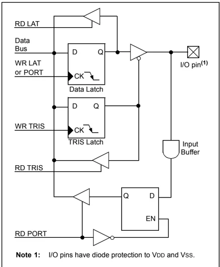
Note 1: I/O pins have diode protection to VDD and Vss.
10.1 PORTA, TRISA and LATA Registers
PORTA is an 8-bit wide, bidirectional port. The corresponding Data Direction register is TRISA. Setting a TRISA bit (= 1) will make the corresponding PORTA pin an input (i.e., put the corresponding output driver in a high-impedance mode). Clearing a TRISA bit (= 0) will make the corresponding PORTA pin an output (i.e., put the contents of the output latch on the selected pin).
Reading the PORTA register reads the status of the pins; writing to it will write to the port latch.
The Data Latch register (LATA) is also memory mapped. Read-modify-write operations on the LATA register read and write the latched output value for PORTA.
The RA4 pin is multiplexed with the Timer0 module clock input to become the RA4/T0CKI pin. The RA6 pin is multiplexed with the main oscillator pin; it is enabled as an oscillator or I/O pin by the selection of the main oscillator in Configuration Register 1H (see Section 25.1 “Configuration Bits” for details). When not used as a port pin, RA6 and its associated TRIS and LAT bits are read as ‘0’.
RA4 is also multiplexed with the USB module; it serves as a receiver input from an external USB transceiver. For details on configuration of the USB module, see Section 17.2 “USB Status and Control”.
Several PORTA pins are multiplexed with analog inputs, the analog VREF+ and VREF- inputs and the comparator voltage reference output. The operation of pins RA5 and RA3:RA0 as A/D converter inputs is selected by clearing/setting the control bits in the ADCON1 register (A/D Control Register 1).
Note: On a Power-on Reset, RA5 and RA3:RA0 are configured as analog inputs and read as ‘0’. RA4 is configured as a digital input.
All other PORTA pins have TTL input levels and full CMOS output drivers.
The TRISA register controls the direction of the RA pins, even when they are being used as analog inputs. The user must ensure the bits in the TRISA register are maintained set when using them as analog inputs.
EXAMPLE 10-1: INITIALIZING PORTA
| CLRF PORTA | ; Initialize PORTA by |
|---|---|
| ; clearing output | |
| ; data latches | |
| CLRF LATA | ; Alternate method |
| ; to clear output | |
| ; data latches | |
| MOVLW 0Fh | ; Configure A/D |
| MOVWF ADCON1 | ; for digital inputs |
| MOVLW 07h | ; Configure comparators |
| MOVWF CMCON | ; for digital input |
| MOVLW 0CFh | ; Value used to |
| ; initialize data | |
| ; direction | |
| MOVWF TRISA | ; Set RA<3:0> as inputs |
| ; RA<5:4> as outputs |
TABLE 10-1: PORTA I/O SUMMARY
| Pin | Function | TRIS Setting | I/O | I/O Type | Description |
|---|---|---|---|---|---|
| RA0/AN0 | RA0 | 0 | OUT | DIG | LATA<0> data output; not affected by analog input. |
| 1 | IN | TTL | PORTA<0> data input; disabled when analog input enabled. | ||
| AN0 | 1 | IN | ANA | A/D Input Channel 0 and Comparator C1- input. Default configuration on POR; does not affect digital output. | |
| RA1/AN1 | RA1 | 0 | OUT | DIG | LATA<1> data output; not affected by analog input. |
| 1 | IN | TTL | PORTA<1> data input; reads ‘0’ on POR. | ||
| AN1 | 1 | IN | ANA | A/D Input Channel 1 and Comparator C2- input. Default configuration on POR; does not affect digital output. | |
| RA2/AN2/VREF-/CVREF | RA2 | 0 | OUT | DIG | LATA<2> data output; not affected by analog input. Disabled when CVREF output enabled. |
| 1 | IN | TTL | PORTA<2> data input. Disabled when analog functions enabled; disabled when CVREF output enabled. | ||
| AN2 | 1 | IN | ANA | A/D Input Channel 2 and Comparator C2+ input. Default configuration on POR; not affected by analog output. | |
| VREF- | 1 | IN | ANA | A/D and comparator voltage reference low input. | |
| CVREF | x | OUT | ANA | Comparator voltage reference output. Enabling this feature disables digital I/O. | |
| RA3/AN3/VREF+ | RA3 | 0 | OUT | DIG | LATA<3> data output; not affected by analog input. |
| 1 | IN | TTL | PORTA<3> data input; disabled when analog input enabled. | ||
| AN3 | 1 | IN | ANA | A/D Input Channel 3 and Comparator C1+ input. Default configuration on POR. | |
| VREF+ | 1 | IN | ANA | A/D and comparator voltage reference high input. | |
| RA4/T0CKI/C1OUT/RCV | RA4 | 0 | OUT | DIG | LATA<4> data output; not affected by analog input. |
| 1 | IN | ST | PORTA<4> data input; disabled when analog input enabled. | ||
| T0CKI | 1 | IN | ST | Timer0 clock input. | |
| C1OUT | 0 | OUT | DIG | Comparator 1 output; takes priority over port data. | |
| RCV | x | IN | TTL | External USB transceiver RCV input. | |
| RA5/AN4/SS/HLVDIN/C2OUT | RA5 | 0 | OUT | DIG | LATA<5> data output; not affected by analog input. |
| 1 | IN | TTL | PORTA<5> data input; disabled when analog input enabled. | ||
| AN4 | 1 | IN | ANA | A/D Input Channel 4. Default configuration on POR. | |
| SS | 1 | IN | TTL | Slave select input for MSSP module. | |
| HLVDIN | 1 | IN | ANA | High/Low-Voltage Detect external trip point input. | |
| C2OUT | 0 | OUT | DIG | Comparator 2 output; takes priority over port data. | |
| OSC2/CLKO/RA6 | OSC2 | x | OUT | ANA | Main oscillator feedback output connection (all XT and HS modes). |
| CLKO | x | OUT | DIG | System cycle clock output (Fosc/4); available in EC, ECPLL and INTCKO modes. | |
| RA6 | 0 | OUT | DIG | LATA<6> data output. Available only in ECIO, ECPIO and INTIO modes; otherwise, reads as ‘0’. | |
| 1 | IN | TTL | PORTA<6> data input. Available only in ECIO, ECPIO and INTIO modes; otherwise, reads as ‘0’. |
Legend: OUT = Output, IN = Input, ANA = Analog Signal, DIG = Digital Output, ST = Schmitt Buffer Input, TTL = TTL Buffer Input, x = Don’t care (TRIS bit does not affect port direction or is overridden for this option)
TABLE 10-2: SUMMARY OF REGISTERS ASSOCIATED WITH PORTA
| Name | Bit 7 | Bit 6 | Bit 5 | Bit 4 | Bit 3 | Bit 2 | Bit 1 | Bit 0 | Reset Values on page |
|---|---|---|---|---|---|---|---|---|---|
| PORTA | — | RA6⁽¹⁾ | RA5 | RA4 | RA3 | RA2 | RA1 | RA0 | 56 |
| LATA | — | LATA6⁽¹⁾ | LATA5 | LATA4 | LATA3 | LATA2 | LATA1 | LATA0 | 56 |
| TRISA | — | TRISA6⁽¹⁾ | TRISA5 | TRISA4 | TRISA3 | TRISA2 | TRISA1 | TRISA0 | 56 |
| ADCON1 | — | — | VCFG1 | VCFG0 | PCFG3 | PCFG2 | PCFG1 | PCFG0 | 54 |
| CMCON | C2OUT | C1OUT | C2INV | C1INV | CIS | CM2 | CM1 | CM0 | 55 |
| CVRCON | CVREN | CVROE | CVRR | CVRSS | CVR3 | CVR2 | CVR1 | CVR0 | 55 |
| UCON | — | PPBRST | SE0 | PKTDIS | USBEN | RESUME | SUSPND | — | 57 |
Legend: — = unimplemented, read as ‘0’. Shaded cells are not used by PORTA.
Note 1: RA6 and its associated latch and data direction bits are enabled as I/O pins based on oscillator configuration; otherwise, they are read as ‘0’.
10.2 PORTB, TRISB and LATB Registers
PORTB is an 8-bit wide, bidirectional port. The corresponding Data Direction register is TRISB. Setting a TRISB bit (= 1) will make the corresponding PORTB pin an input (i.e., put the corresponding output driver in a high-impedance mode). Clearing a TRISB bit (= 0) will make the corresponding PORTB pin an output (i.e., put the contents of the output latch on the selected pin).
The Data Latch register (LATB) is also memory mapped. Read-modify-write operations on the LATB register read and write the latched output value for PORTB.
Each of the PORTB pins has a weak internal pull-up. A single control bit can turn on all the pull-ups. This is performed by clearing bit, \overlineRBPU (INTCON2<7>). The weak pull-up is automatically turned off when the port pin is configured as an output. The pull-ups are disabled on a Power-on Reset.
Note: On a Power-on Reset, RB4:RB0 are configured as analog inputs by default and read as '0'; RB7:RB5 are configured as digital inputs.
By programming the Configuration bit, PBADEN (CONFIG3H<1>), RB4:RB0 will alternatively be configured as digital inputs on POR.
Four of the PORTB pins (RB7:RB4) have an interrupt-on-change feature. Only pins configured as inputs can cause this interrupt to occur. Any RB7:RB4 pin configured as an output is excluded from the interrupt-on-change comparison. The pins are compared with the old value latched on the last read of PORTB. The "mismatch" outputs of RB7:RB4 are ORed together to generate the RB Port Change Interrupt with Flag bit, RBIF (INTCON<0>).
The interrupt-on-change can be used to wake the device from Sleep. The user, in the Interrupt Service Routine, can clear the interrupt in the following manner: a) Any read or write of PORTB (except with the MOVFF (ANY), PORTB instruction). This will end the mismatch condition. b) Wait one Tcy delay (for example, execute one NOP instruction). c) Clear flag bit, RBIF
A mismatch condition will continue to set flag bit, RBIF. Reading PORTB will end the mismatch condition and allow flag bit, RBIF, to be cleared after a one Tcy delay.
The interrupt-on-change feature is recommended for wake-up on key depression operation and operations where PORTB is only used for the interrupt-on-change feature. Polling of PORTB is not recommended while using the interrupt-on-change feature.
Pins, RB2 and RB3, are multiplexed with the USB peripheral and serve as the differential signal outputs for an external USB transceiver (TRIS configuration). Refer to Section 17.2.2.2 "External Transceiver" for additional information on configuring the USB module for operation with an external transceiver.
RB4 is multiplexed with CSSPP, the chip select function for the Streaming Parallel Port (SPP) – TRIS setting. Details of its operation are discussed in Section 18.0 "Streaming Parallel Port".
EXAMPLE 10-2: INITIALIZING PORTB
\begin{tabular}{lll} CLRF & PORTB & ; Initialize PORTB by \ & & ; clearing output \ & & ; data latches \ CLRF & LATB & ; Alternate method \ & & ; to clear output \ & & ; data latches \ MOVLW & 0Eh & ; Set RB<4:0> as \ MOVWF & ADCON1 & ; digital I/O pins \ & & ; (required if config bit \ & & ; PBADEN is set) \ MOVLW & 0CFh & ; Value used to \ & & ; initialize data \ & & ; direction \ MOVWF & TRISB & ; Set RB<3:0> as inputs \ & & ; RB<5:4> as outputs \ & & ; RB<7:6> as inputs \ \end{tabular}
DS39632E-page 116 © 2009 Microchip Technology Inc.
TABLE 10-3: PORTB I/O SUMMARY
| Pin | Function | TRIS Setting | I/O | I/O Type | Description |
|---|---|---|---|---|---|
| RB0/AN12/INT0/FLT0/SDI/SDA | RB0 | 0 | OUT | DIG | LATB<0> data output; not affected by analog input. |
| 1 | IN | TTL | PORTB<0> data input; weak pull-up when RBPU bit is cleared. Disabled when analog input enabled.(1) | ||
| AN12 | 1 | IN | ANA | A/D Input Channel 12.(1) | |
| INT0 | 1 | IN | ST | External Interrupt 0 input. | |
| FLT0 | 1 | IN | ST | Enhanced PWM Fault input (ECCP1 module); enabled in software. | |
| SDI | 1 | IN | ST | SPI data input (MSSP module). | |
| SDA | 1 | OUT | DIG | I²C™ data output (MSSP module); takes priority over port data. | |
| 1 | IN | I²C/SMB | I²C data input (MSSP module); input type depends on module setting. | ||
| RB1/AN10/INT1/SCK/SCL | RB1 | 0 | OUT | DIG | LATB<1> data output; not affected by analog input. |
| 1 | IN | TTL | PORTB<1> data input; weak pull-up when RBPU bit is cleared. Disabled when analog input enabled.(1) | ||
| AN10 | 1 | IN | ANA | A/D Input Channel 10.(1) | |
| INT1 | 1 | IN | ST | External Interrupt 1 input. | |
| SCK | 0 | OUT | DIG | SPI clock output (MSSP module); takes priority over port data. | |
| 1 | IN | ST | SPI clock input (MSSP module). | ||
| SCL | 0 | OUT | DIG | I²C clock output (MSSP module); takes priority over port data. | |
| 1 | IN | I²C/SMB | I²C clock input (MSSP module); input type depends on module setting. | ||
| RB2/AN8/INT2/VMO | RB2 | 0 | OUT | DIG | LATB<2> data output; not affected by analog input. |
| 1 | IN | TTL | PORTB<2> data input; weak pull-up when RBPU bit is cleared. Disabled when analog input enabled.(1) | ||
| AN8 | 1 | IN | ANA | A/D input channel 8.(1) | |
| INT2 | 1 | IN | ST | External Interrupt 2 input. | |
| VMO | 0 | OUT | DIG | External USB transceiver VMO data output. | |
| RB3/AN9/CCP2/VPO | RB3 | 0 | OUT | DIG | LATB<3> data output; not affected by analog input. |
| 1 | IN | TTL | PORTB<3> data input; weak pull-up when RBPU bit is cleared. Disabled when analog input enabled.(1) | ||
| AN9 | 1 | IN | ANA | A/D Input Channel 9.(1) | |
| CCP2(2) | 0 | OUT | DIG | CCP2 compare and PWM output. | |
| 1 | IN | ST | CCP2 capture input. | ||
| VPO | 0 | OUT | DIG | External USB transceiver VPO data output. | |
| RB4/AN11/KBIO/CSSPP | RB4 | 0 | OUT | DIG | LATB<4> data output; not affected by analog input. |
| 1 | IN | TTL | PORTB<4> data input; weak pull-up when RBPU bit is cleared. Disabled when analog input enabled.(1) | ||
| AN11 | 1 | IN | ANA | A/D Input Channel 11.(1) | |
| KBIO | 1 | IN | TTL | Interrupt-on-pin change. | |
| CSSPP(4) | 0 | OUT | DIG | SPP chip select control output. | |
| RB5/KBI1/PGM | RB5 | 0 | OUT | DIG | LATB<5> data output. |
| 1 | IN | TTL | PORTB<5> data input; weak pull-up when RBPU bit is cleared. | ||
| KBI1 | 1 | IN | TTL | Interrupt-on-pin change. | |
| PGM | x | IN | ST | Single-Supply Programming mode entry (ICSP™). Enabled by LVP Configuration bit; all other pin functions disabled. |
Legend: OUT = Output, IN = Input, ANA = Analog Signal, DIG = Digital Output, ST = Schmitt Buffer Input, I²C/SMB = I²C/SMBus input buffer, TTL = TTL Buffer Input, x = Don’t care (TRIS bit does not affect port direction or is overridden for this option)
Note 1: Configuration on POR is determined by PBADEN Configuration bit. Pins are configured as analog inputs when PBADEN is set and digital inputs when PBADEN is cleared.
2: Alternate pin assignment for CCP2 when CCP2MX = 0. Default assignment is RC1.
3: All other pin functions are disabled when ICSP™ or ICD operation is enabled.
4: 40/44-pin devices only.
TABLE 10-3: PORTB I/O SUMMARY (CONTINUED)
| Pin | Function | TRIS Setting | I/O | I/O Type | Description |
|---|---|---|---|---|---|
| RB6/KBI2/PGC | RB6 | 0 | OUT | DIG | LATB<6> data output. |
| 1 | IN | TTL | PORTB<6> data input; weak pull-up when RBPU bit is cleared. | ||
| KBI2 | 1 | IN | TTL | Interrupt-on-pin change. | |
| PGC | x | IN | ST | Serial execution (ICSP™) clock input for ICSP and ICD operation.(3) | |
| RB7/KBI3/PGD | RB7 | 0 | OUT | DIG | LATB<7> data output. |
| 1 | IN | TTL | PORTB<7> data input; weak pull-up when RBPU bit is cleared. | ||
| KBI3 | 1 | IN | TTL | Interrupt-on-pin change. | |
| PGD | x | OUT | DIG | Serial execution data output for ICSP and ICD operation.(3) | |
| x | IN | ST | Serial execution data input for ICSP and ICD operation.(3) |
Legend: OUT = Output, IN = Input, ANA = Analog Signal, DIG = Digital Output, ST = Schmitt Buffer Input, I²C/SMB = I²C/SMBus input buffer, TTL = TTL Buffer Input, x = Don’t care (TRIS bit does not affect port direction or is overridden for this option)
Note 1: Configuration on POR is determined by PBADEN Configuration bit. Pins are configured as analog inputs when PBADEN is set and digital inputs when PBADEN is cleared.
2: Alternate pin assignment for CCP2 when CCP2MX = 0. Default assignment is RC1.
3: All other pin functions are disabled when ICSP™ or ICD operation is enabled.
4: 40/44-pin devices only.
TABLE 10-4: SUMMARY OF REGISTERS ASSOCIATED WITH PORTB
| Name | Bit 7 | Bit 6 | Bit 5 | Bit 4 | Bit 3 | Bit 2 | Bit 1 | Bit 0 | Reset Values on page |
|---|---|---|---|---|---|---|---|---|---|
| PORTB | RB7 | RB6 | RB5 | RB4 | RB3 | RB2 | RB1 | RB0 | 56 |
| LATB | LATB7 | LATB6 | LATB5 | LATB4 | LATB3 | LATB2 | LATB1 | LATB0 | 56 |
| TRISB | TRISB7 | TRISB6 | TRISB5 | TRISB4 | TRISB3 | TRISB2 | TRISB1 | TRISB0 | 56 |
| INTCON | GIE/GIEH | PEIE/GIEL | TMR0IE | INT0IE | RBIE | TMR0IF | INT0IF | RBIF | 53 |
| INTCON2 | RBPU | INTEDG0 | INTEDG1 | INTEDG2 | — | TMR0IP | — | RBIP | 53 |
| INTCON3 | INT2IP | INT1IP | — | INT2IE | INT1IE | — | INT2IF | INT1IF | 53 |
| ADCON1 | — | — | VCFG1 | VCFG0 | PCFG3 | PCFG2 | PCFG1 | PCFG0 | 54 |
| SPPCON(1) | — | — | — | — | — | — | SPPOWN | SPPEN | 57 |
| SPPCFG(1) | CLKCFG1 | CLKCFG0 | CSEN | CLK1EN | WS3 | WS2 | WS1 | WS0 | 57 |
| UCON | — | PPBRST | SE0 | PKTDIS | USBEN | RESUME | SUSPND | — | 57 |
Legend: — = unimplemented, read as ‘0’. Shaded cells are not used by PORTB.
Note 1: These registers are unimplemented on 28-pin devices.
10.3 PORTC, TRISC and LATC Registers
PORTC is a 7-bit wide, bidirectional port. The corresponding Data Direction register is TRISC. Setting a TRISC bit (= 1) will make the corresponding PORTC pin an input (i.e., put the corresponding output driver in a high-impedance mode). Clearing a TRISC bit (= 0) will make the corresponding PORTC pin an output (i.e., put the contents of the output latch on the selected pin).
The RC3 pin is not implemented in these devices.
The Data Latch register (LATC) is also memory mapped. Read-modify-write operations on the LATC register read and write the latched output value for PORTC.
PORTC is primarily multiplexed with serial communication modules, including the EUSART, MSSP module and the USB module (Table 10-5). Except for RC4 and RC5, PORTC uses Schmitt Trigger input buffers.
Pins RC4 and RC5 are multiplexed with the USB module. Depending on the configuration of the module, they can serve as the differential data lines for the on-chip USB transceiver, or the data inputs from an external USB transceiver. Both RC4 and RC5 have TTL input buffers instead of the Schmitt Trigger buffers on the other pins.
Unlike other PORTC pins, RC4 and RC5 do not have TRISC bits associated with them. As digital ports, they can only function as digital inputs. When configured for USB operation, the data direction is determined by the configuration and status of the USB module at a given time. If an external transceiver is used, RC4 and RC5 always function as inputs from the transceiver. If the on-chip transceiver is used, the data direction is determined by the operation being performed by the module at that time.
When the external transceiver is enabled, RC2 also serves as the output enable control to the transceiver. Additional information on configuring USB options is provided in Section 17.2.2.2 "External Transceiver".
When enabling peripheral functions on PORTC pins other than RC4 and RC5, care should be taken in defining the TRIS bits. Some peripherals override the TRIS bit to make a pin an output, while other peripherals override the TRIS bit to make a pin an input. The user should refer to the corresponding peripheral section for the correct TRIS bit settings.
Note: On a Power-on Reset, these pins, except RC4 and RC5, are configured as digital inputs. To use pins RC4 and RC5 as digital inputs, the USB module must be disabled (UCON<3> = 0) and the on-chip USB transceiver must be disabled (UCFG<3> = 1).
The contents of the TRISC register are affected by peripheral overrides. Reading TRISC always returns the current contents, even though a peripheral device may be overriding one or more of the pins.
EXAMPLE 10-3: INITIALIZING PORTC CLRF PORTC ; Initialize PORTC by ; clearing output ; data latches CLRF LATC ; Alternate method ; to clear output ; data latches MOVLW 07h ; Value used to ; initialize data ; direction MOVWF TRISC ; RC<5:0> as outputs ; RC<7:6> as inputs
TABLE 10-5: PORTC I/O SUMMARY
| Pin | Function | TRIS Setting | I/O | I/O Type | Description |
|---|---|---|---|---|---|
| RC0/T1OSO/T13CKI | RC0 | 0 | OUT | DIG | LATC<0> data output. |
| 1 | IN | ST | PORTC<0> data input. | ||
| T1OSO | x | OUT | ANA | Timer1 oscillator output; enabled when Timer1 oscillator enabled. Disables digital I/O. | |
| T13CKI | 1 | IN | ST | Timer1/Timer3 counter input. | |
| RC1/T1OSI/CCP2/UOE | RC1 | 0 | OUT | DIG | LATC<1> data output. |
| 1 | IN | ST | PORTC<1> data input. | ||
| T1OSI | x | IN | ANA | Timer1 oscillator input; enabled when Timer1 oscillator enabled. Disables digital I/O. | |
| CCP2(1) | 0 | OUT | DIG | CCP2 compare and PWM output; takes priority over port data. | |
| 1 | IN | ST | CCP2 capture input. | ||
| UOE | 0 | OUT | DIG | External USB transceiver OE output. | |
| RC2/CCP1/P1A | RC2 | 0 | OUT | DIG | LATC<2> data output. |
| 1 | IN | ST | PORTC<2> data input. | ||
| CCP1 | 0 | OUT | DIG | ECCP1 compare and PWM output; takes priority over port data. | |
| 1 | IN | ST | ECCP1 capture input. | ||
| P1A(3) | 0 | OUT | DIG | ECCP1 Enhanced PWM output, Channel A; takes priority over port data. May be configured for tri-state during Enhanced PWM shutdown events. | |
| RC4/D-/VM | RC4 | __(2) | IN | TTL | PORTC<4> data input; disabled when USB module or on-chip transceiver are enabled. |
| D- | __(2) | OUT | XCVR | USB bus differential minus line output (internal transceiver). | |
| __(2) | IN | XCVR | USB bus differential minus line input (internal transceiver). | ||
| VM | __(2) | IN | TTL | External USB transceiver VM input. | |
| RC5/D+/VP | RC5 | __(2) | IN | TTL | PORTC<5> data input; disabled when USB module or on-chip transceiver are enabled. |
| D+ | __(2) | OUT | XCVR | USB bus differential plus line output (internal transceiver). | |
| __(2) | IN | XCVR | USB bus differential plus line input (internal transceiver). | ||
| VP | __(2) | IN | TTL | External USB transceiver VP input. | |
| RC6/TX/CK | RC6 | 0 | OUT | DIG | LATC<6> data output. |
| 1 | IN | ST | PORTC<6> data input. | ||
| TX | 0 | OUT | DIG | Asynchronous serial transmit data output (EUSART module); takes priority over port data. User must configure as output. | |
| CK | 0 | OUT | DIG | Synchronous serial clock output (EUSART module); takes priority over port data. | |
| 1 | IN | ST | Synchronous serial clock input (EUSART module). |
Legend: OUT = Output, IN = Input, ANA = Analog Signal, DIG = Digital Output, ST = Schmitt Buffer Input, TTL = TTL Buffer Input, XCVR = USB transceiver, x = Don’t care (TRIS bit does not affect port direction or is overridden for this option)
Note 1: Default pin assignment. Alternate pin assignment is RB3 (when CCP2MX = 0).
Note 2: RC4 and RC5 do not have corresponding TRISC bits. In Port mode, these pins are input only. USB data direction is determined by the USB configuration.
Note 3: 40/44-pin devices only.
TABLE 10-5: PORTC I/O SUMMARY (CONTINUED)
| Pin | Function | TRIS Setting | I/O | I/O Type | Description |
|---|---|---|---|---|---|
| RC7/RX/DT/SDO | RC7 | 0 | OUT | DIG | LATC<7> data output. |
| 1 | IN | ST | PORTC<7> data input. | ||
| RX | 1 | IN | ST | Asynchronous serial receive data input (EUSART module). | |
| DT | 1 | OUT | DIG | Synchronous serial data output (EUSART module); takes priority over SPI and port data. | |
| 1 | IN | ST | Synchronous serial data input (EUSART module). User must configure as an input. | ||
| SDO | 0 | OUT | DIG | SPI data output (MSSP module); takes priority over port data. |
Legend: OUT = Output, IN = Input, ANA = Analog Signal, DIG = Digital Output, ST = Schmitt Buffer Input, TTL = TTL Buffer Input, XCVR = USB transceiver, x = Don’t care (TRIS bit does not affect port direction or is overridden for this option)
Note 1: Default pin assignment. Alternate pin assignment is RB3 (when CCP2MX = 0).
Note 2: RC4 and RC5 do not have corresponding TRISC bits. In Port mode, these pins are input only. USB data direction is determined by the USB configuration.
Note 3: 40/44-pin devices only.
TABLE 10-6: SUMMARY OF REGISTERS ASSOCIATED WITH PORTC
| Name | Bit 7 | Bit 6 | Bit 5 | Bit 4 | Bit 3 | Bit 2 | Bit 1 | Bit 0 | Reset Values on page |
|---|---|---|---|---|---|---|---|---|---|
| PORTC | RC7 | RC6 | RC5(1) | RC4(1) | — | RC2 | RC1 | RC0 | 56 |
| LATC | LATC7 | LATC6 | — | — | — | LATC2 | LATC1 | LATC0 | 56 |
| TRISC | TRISC7 | TRISC6 | — | — | — | TRISC2 | TRISC1 | TRISC0 | 56 |
| UCON | — | PPBRST | SE0 | PKTDIS | USBEN | RESUME | SUSPND | — | 57 |
Legend: — = unimplemented, read as ‘0’. Shaded cells are not used by PORTC.
Note 1: RC5 and RC4 are only available as port pins when the USB module is disabled (UCON<3> = 0).
10.4 PORTD, TRISD and LATD Registers
Note: PORTD is only available on 40/44-pin devices.
PORTD is an 8-bit wide, bidirectional port. The corresponding Data Direction register is TRISD. Setting a TRISD bit (= 1) will make the corresponding PORTD pin an input (i.e., put the corresponding output driver in a high-impedance mode). Clearing a TRISD bit (= 0) will make the corresponding PORTD pin an output (i.e., put the contents of the output latch on the selected pin).
The Data Latch register (LATD) is also memory mapped. Read-modify-write operations on the LATD register read and write the latched output value for PORTD.
All pins on PORTD are implemented with Schmitt Trigger input buffers. Each pin is individually configurable as an input or output.
Each of the PORTD pins has a weak internal pull-up. A single control bit, RDPU (PORTE<7>), can turn on all the pull-ups. This is performed by setting RDPU. The weak pull-up is automatically turned off when the port pin is configured as a digital output or as one of the other multiplexed peripherals. The pull-ups are disabled on a Power-on Reset. The PORTE register is shown in Section 10.5 “PORTE, TRISE and LATE Registers”.
Three of the PORTD pins are multiplexed with outputs, P1B, P1C and P1D, of the Enhanced CCP module. The operation of these additional PWM output pins is covered in greater detail in Section 16.0 “Enhanced Capture/Compare/PWM (ECCP) Module”.
Note: On a Power-on Reset, these pins are configured as digital inputs.
PORTD can also be configured as an 8-bit wide Streaming Parallel Port (SPP). In this mode, the input buffers are TTL. For additional information on configuration and uses of the SPP, see Section 18.0 “Streaming Parallel Port”..
Note: When the Enhanced PWM mode is used with either dual or quad outputs, the MSSP functions of PORTD are automatically disabled.
EXAMPLE 10-4: INITIALIZING PORTD
TABLE 10-7: PORTD I/O SUMMARY
| Pin | Function | TRIS Setting | I/O | I/O Type | Description |
|---|---|---|---|---|---|
| RD0/SPP0 | RD0 | 0 | OUT | DIG | LATD<0> data output. |
| 1 | IN | ST | PORTD<0> data input. | ||
| SPP0 | 1 | OUT | DIG | SPP<0> output data; takes priority over port data. | |
| 1 | IN | TTL | SPP<0> input data. | ||
| RD1/SPP1 | RD1 | 0 | OUT | DIG | LATD<1> data output. |
| 1 | IN | ST | PORTD<1> data input. | ||
| SPP1 | 1 | OUT | DIG | SPP<1> output data; takes priority over port data. | |
| 1 | IN | TTL | SPP<1> input data. | ||
| RD2/SPP2 | RD2 | 0 | OUT | DIG | LATD<2> data output. |
| 1 | IN | ST | PORTD<2> data input. | ||
| SPP2 | 1 | OUT | DIG | SPP<2> output data; takes priority over port data. | |
| 1 | IN | TTL | SPP<2> input data. | ||
| RD3/SPP3 | RD3 | 0 | OUT | DIG | LATD<3> data output. |
| 1 | IN | ST | PORTD<3> data input. | ||
| SPP3 | 1 | OUT | DIG | SPP<3> output data; takes priority over port data. | |
| 1 | IN | TTL | SPP<3> input data. | ||
| RD4/SPP4 | RD4 | 0 | OUT | DIG | LATD<4> data output. |
| 1 | IN | ST | PORTD<4> data input. | ||
| SPP4 | 1 | OUT | DIG | SPP<4> output data; takes priority over port data. | |
| 1 | IN | TTL | SPP<4> input data. | ||
| RD5/SPP5/P1B | RD5 | 0 | OUT | DIG | LATD<5> data output |
| 1 | IN | ST | PORTD<5> data input | ||
| SPP5 | 1 | OUT | DIG | SPP<5> output data; takes priority over port data. | |
| 1 | IN | TTL | SPP<5> input data. | ||
| P1B | 0 | OUT | DIG | ECCP1 Enhanced PWM output, Channel B; takes priority over port and SPP data.(1) | |
| RD6/SPP6/P1C | RD6 | 0 | OUT | DIG | LATD<6> data output. |
| 1 | IN | ST | PORTD<6> data input. | ||
| SPP6 | 1 | OUT | DIG | SPP<6> output data; takes priority over port data. | |
| 1 | IN | TTL | SPP<6> input data. | ||
| P1C | 0 | OUT | DIG | ECCP1 Enhanced PWM output, Channel C; takes priority over port and SPP data.(1) | |
| RD7/SPP7/P1D | RD7 | 0 | OUT | DIG | LATD<7> data output. |
| 1 | IN | ST | PORTD<7> data input. | ||
| SPP7 | 1 | OUT | DIG | SPP<7> output data; takes priority over port data. | |
| 1 | IN | TTL | SPP<7> input data. | ||
| P1D | 0 | OUT | DIG | ECCP1 Enhanced PWM output, Channel D; takes priority over port and SPP data.(1) |
Legend: OUT = Output, IN = Input, DIG = Digital Output, ST = Schmitt Buffer Input, TTL = TTL Buffer Input
Note 1: May be configured for tri-state during Enhanced PWM shutdown events.
TABLE 10-8: SUMMARY OF REGISTERS ASSOCIATED WITH PORTD
| Name | Bit 7 | Bit 6 | Bit 5 | Bit 4 | Bit 3 | Bit 2 | Bit 1 | Bit 0 | Reset Values on page |
|---|---|---|---|---|---|---|---|---|---|
| PORTD(3) | RD7 | RD6 | RD5 | RD4 | RD3 | RD2 | RD1 | RD0 | 56 |
| LATD(3) | LATD7 | LATD6 | LATD5 | LATD4 | LATD3 | LATD2 | LATD1 | LATD0 | 56 |
| TRISD(3) | TRISD7 | TRISD6 | TRISD5 | TRISD4 | TRISD3 | TRISD2 | TRISD1 | TRISD0 | 56 |
| PORTE | RDPU(3) | — | — | — | RE3(1,2) | RE2(3) | RE1(3) | RE0(3) | 56 |
| CCP1CON | P1M1(3) | P1M0(3) | DC1B1 | DC1B0 | CCP1M3 | CCP1M2 | CCP1M1 | CCP1M0 | 55 |
| SPPCON(3) | — | — | — | — | — | — | SPPOWN | SPPEN | 57 |
Legend: — = unimplemented, read as ‘0’. Shaded cells are not used by PORTD.
Note 1: Implemented only when Master Clear functionality is disabled (MCLRE Configuration bit = 0).
2: RE3 is the only PORTE bit implemented on both 28-pin and 40/44-pin devices. All other bits are implemented only when PORTE is implemented (i.e., 40/44-pin devices).
3: These registers and/or bits are unimplemented on 28-pin devices.
10.5 PORTE, TRISE and LATE Registers
Depending on the particular PIC18F2455/2550/4455/4550 device selected, PORTE is implemented in two different ways.
For 40/44-pin devices, PORTE is a 4-bit wide port. Three pins (RE0/AN5/CK1SPP, RE1/AN6/CK2SPP and RE2/AN7/OESPP) are individually configurable as inputs or outputs. These pins have Schmitt Trigger input buffers. When selected as an analog input, these pins will read as ‘0’s.
The corresponding Data Direction register is TRISE. Setting a TRISE bit (= 1) will make the corresponding PORTE pin an input (i.e., put the corresponding output driver in a high-impedance mode). Clearing a TRISE bit (= 0) will make the corresponding PORTE pin an output (i.e., put the contents of the output latch on the selected pin).
In addition to port data, the PORTE register (Register 10-1) also contains the RDPU control bit (PORTE<7>); this enables or disables the weak pull-ups on PORTD.
TRISE controls the direction of the RE pins, even when they are being used as analog inputs. The user must make sure to keep the pins configured as inputs when using them as analog inputs.
Note: On a Power-on Reset, RE2:RE0 are configured as analog inputs.
The Data Latch register (LATE) is also memory mapped. Read-modify-write operations on the LATE register read and write the latched output value for PORTE.
The fourth pin of PORTE (MCLR/VPP/RE3) is an input only pin. Its operation is controlled by the MCLRE Configuration bit. When selected as a port pin (MCLRE = 0), it functions as a digital input only pin; as such, it does not have TRIS or LAT bits associated with its operation. Otherwise, it functions as the device’s Master Clear input. In either configuration, RE3 also functions as the programming voltage input during programming.
Note: On a Power-on Reset, RE3 is enabled as a digital input only if Master Clear functionality is disabled.
EXAMPLE 10-5: INITIALIZING PORTE
CLRF PORTE ; Initialize PORTE by ; clearing output ; data latches CLRF LATE ; Alternate method ; to clear output ; data latches MOVLW 0Ah ; Configure A/D MOVWF ADCON1 ; for digital inputs MOVLW 03h ; Value used to ; initialize data ; direction MOVLW 07h ; Turn off MOVWF CMCON ; comparators MOVWF TRISC ; Set RE<0> as inputs ; RE<1> as outputs ; RE<2> as inputs
10.5.1 PORTE IN 28-PIN DEVICES
For 28-pin devices, PORTE is only available when Master Clear functionality is disabled (MCLRE = 0). In these cases, PORTE is a single bit, input only port comprised of RE3 only. The pin operates as previously described.
REGISTER 10-1: PORTE REGISTER
| R/W-0 | U-0 | U-0 | U-0 | R/W-x | R/W-0 | R/W-0 | R/W-0 |
|---|---|---|---|---|---|---|---|
| RDPU(3) | — | — | — | RE3(1,2) | RE2(3) | RE1(3) | RE0(3) |
| bit 7 | bit 0 |
Legend:
R = Readable bit
W = Writable bit
U = Unimplemented bit, read as ‘0’
-n = Value at POR
‘1’ = Bit is set
‘0’ = Bit is cleared
x = Bit is unknown
bit 7
RDPU: PORTD Pull-up Enable bit
1 = PORTD pull-ups are enabled by individual port latch values
0 = All PORTD pull-ups are disabled
bit 6-4
Unimplemented: Read as ‘0’
bit 3-0
RE3:RE0: PORTE Data Input bits(1,2,3)
Note 1: implemented only when Master Clear functionality is disabled (MCLRE Configuration bit = 0); otherwise, read as ‘0’.
2: RE3 is the only PORTE bit implemented on both 28-pin and 40/44-pin devices. All other bits are implemented only when PORTE is implemented (i.e., 40/44-pin devices).
3: Unimplemented in 28-pin devices; read as ‘0’.
TABLE 10-9: PORTE I/O SUMMARY
| Pin | Function | TRIS Setting | I/O | I/O Type | Description |
|---|---|---|---|---|---|
| RE0/AN5/CK1SPP | RE0 | 0 | OUT | DIG | LATE<0> data output; not affected by analog input. |
| 1 | IN | ST | PORTE<0> data input; disabled when analog input enabled. | ||
| AN5 | 1 | IN | ANA | A/D Input Channel 5; default configuration on POR. | |
| CK1SPP | 0 | OUT | DIG | SPP clock 1 output (SPP enabled). | |
| RE1/AN6/CK2SPP | RE1 | 0 | OUT | DIG | LATE<1> data output; not affected by analog input. |
| 1 | IN | ST | PORTE<1> data input; disabled when analog input enabled. | ||
| AN6 | 1 | IN | ANA | A/D Input Channel 6; default configuration on POR. | |
| CK2SPP | 0 | OUT | DIG | SPP clock 2 output (SPP enabled). | |
| RE2/AN7/OESPP | RE2 | 0 | OUT | DIG | LATE<2> data output; not affected by analog input. |
| 1 | IN | ST | PORTE<2> data input; disabled when analog input enabled. | ||
| AN7 | 1 | IN | ANA | A/D Input Channel 7; default configuration on POR. | |
| OESPP | 0 | OUT | DIG | SPP enable output (SPP enabled). | |
| MCLR/VPP/RE3 | MCLR | —(1) | IN | ST | External Master Clear input; enabled when MCLRE Configuration bit is set. |
| VPP | —(1) | IN | ANA | High-voltage detection, used for ICSP™ mode entry detection. Always available regardless of pin mode. | |
| RE3 | —(1) | IN | ST | PORTE<3> data input; enabled when MCLRE Configuration bit is clear. |
Legend: OUT = Output, IN = Input, ANA = Analog Signal, DIG = Digital Output, ST = Schmitt Buffer Input
Note 1: RE3 does not have a corresponding TRISE<3> bit. This pin is always an input regardless of mode.
TABLE 10-10: SUMMARY OF REGISTERS ASSOCIATED WITH PORTE
| Name | Bit 7 | Bit 6 | Bit 5 | Bit 4 | Bit 3 | Bit 2 | Bit 1 | Bit 0 | Reset Values on page |
|---|---|---|---|---|---|---|---|---|---|
| PORTE | RDPU(3) | — | — | — | RE3(1,2) | RE2(3) | RE1(3) | RE0(3) | 56 |
| LATE(3) | — | — | — | — | — | LATE2 | LATE1 | LATE0 | 56 |
| TRISE(3) | — | — | — | — | — | TRISE2 | TRISE1 | TRISE0 | 56 |
| ADCON1 | — | — | VCFG1 | VCFG0 | PCFG3 | PCFG2 | PCFG1 | PCFG0 | 54 |
| CMCON | C2OUT | C1OUT | C2INV | C1INV | CIS | CM2 | CM1 | CM0 | 55 |
| SPPCON(3) | — | — | — | — | — | — | SPPOWN | SPPEN | 57 |
| SPPCFG(3) | CLKCFG1 | CLKCFG0 | CSEN | CLK1EN | WS3 | WS2 | WS1 | WS0 | 57 |
Legend: — = unimplemented, read as ‘0’. Shaded cells are not used by PORTE.
Note 1: Implemented only when Master Clear functionality is disabled (MCLRE Configuration bit = 0).
2: RE3 is the only PORTE bit implemented on both 28-pin and 40/44-pin devices. All other bits are implemented only when PORTE is implemented (i.e., 40/44-pin devices).
3: These registers or bits are unimplemented on 28-pin devices.