22.0 COMPARATOR MODULE
The analog comparator module contains two comparators that can be configured in a variety of ways. The inputs can be selected from the analog inputs multiplexed with pins RA0 through RA5, as well as the on-chip voltage reference (see Section 23.0 “Comparator Voltage Reference Module”). The digital outputs (normal or inverted) are available at the pin level and can also be read through the control register.
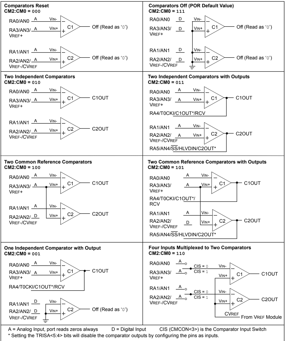
The CMCON register (Register 22-1) selects the comparator input and output configuration. Block diagrams of the various comparator configurations are shown in Figure 22-1.
REGISTER 22-1: CMCON: COMPARATOR CONTROL REGISTER
| R-0 | R-0 | R/W-0 | R/W-0 | R/W-0 | R/W-1 | R/W-1 | R/W-1 |
|---|---|---|---|---|---|---|---|
| C2OUT | C1OUT | C2INV | C1INV | CIS | CM2 | CM1 | CM0 |
| bit 7 | bit 0 |
Legend:
R = Readable bit
W = Writable bit
U = Unimplemented bit, read as ‘0’
-n = Value at POR
‘1’ = Bit is set
‘0’ = Bit is cleared
x = Bit is unknown
bit 7
C2OUT: Comparator 2 Output bit
When C2INV = 0:
1 = C2 VIN+ > C2 VIN-
0 = C2 VIN+ < C2 VIN-
When C2INV = 1:
1 = C2 VIN+ < C2 VIN-
0 = C2 VIN+ > C2 VIN-
bit 6
C1OUT: Comparator 1 Output bit
When C1INV = 0:
1 = C1 VIN+ > C1 VIN-
0 = C1 VIN+ < C1 VIN-
When C1INV = 1:
1 = C1 VIN+ < C1 VIN-
0 = C1 VIN+ > C1 VIN-
bit 5
C2INV: Comparator 2 Output Inversion bit
1 = C2 output inverted
0 = C2 output not inverted
bit 4
C1INV: Comparator 1 Output Inversion bit
1 = C1 output inverted
0 = C1 output not inverted
bit 3
CIS: Comparator Input Switch bit
When CM2:CM0 = 110:
1 = C1 VIN- connects to RA3/AN3/VREF+
C2 VIN- connects to RA2/AN2/VREF-/CVREF
0 = C1 VIN- connects to RA0/AN0
C2 VIN- connects to RA1/AN1
bit 2-0
CM2:CM0: Comparator Mode bits
Figure 22-1 shows the Comparator modes and the CM2:CM0 bit settings.
22.1 Comparator Configuration
There are eight modes of operation for the comparators, shown in Figure 22-1. Bits, CM2:CM0 of the CMCON register, are used to select these modes. The TRISA register controls the data direction of the comparator pins for each mode. If the Comparator mode is changed, the comparator output level may not be valid for the specified mode change delay shown in Section 28.0 “Electrical Characteristics”.
Note: Comparator interrupts should be disabled during a Comparator mode change. Otherwise, a false interrupt may occur.
FIGURE 22-1: COMPARATOR I/O OPERATING MODES
| Comparators Reset CM2:CM0 = 000 | Comparators Off (POR Default Value) CM2:CM0 = 111 |
|---|---|
| RA0/AN0 A VIN-RA3/AN3/ A VIN+VREF+RA1/AN1 A VIN-RA2/AN2/ A VIN+VREF-/CVREF | RA0/AN0 D VIN-RA3/AN3/ D VIN+VREF+RA1/AN1 D VIN-RA2/AN2/ D VIN+VREF-/CVREF |
| Off (Read as ‘0’) | Off (Read as ‘0’) |
| Off (Read as ‘0’) | Off (Read as ‘0’) |
| Two Independent Comparators CM2:CM0 = 010 | Two Independent Comparators with Outputs CM2:CM0 = 011 |
|---|---|
| RA0/AN0 A VIN-RA3/AN3/ A VIN+VREF+RA1/AN1 A VIN-RA2/AN2/ A VIN+VREF-/CVREF | RA0/AN0 A VIN-RA3/AN3/ A VIN+VREF+RA4/T0CKI/C1OUT*/RCVRA1/AN1 A VIN-RA2/AN2/ A VIN+VREF-/CVREFRA5/AN4/SS/HLVDIN/C2OUT* |
| C1OUT | C1OUT |
| C2OUT | C2OUT |
| Two Common Reference Comparators CM2:CM0 = 100 | Two Common Reference Comparators with Outputs CM2:CM0 = 101 |
|---|---|
| RA0/AN0 A VIN-RA3/AN3/ A VIN+VREF+RA1/AN1 A VIN-RA2/AN2/ D VIN+VREF-/CVREF | RA0/AN0 A VIN-RA3/AN3/ A VIN+VREF+RA4/T0CKI/C1OUT*/RCVRA1/AN1 A VIN-RA2/AN2/ D VIN+VREF-/CVREFRA5/AN4/SS/HLVDIN/C2OUT* |
| C1OUT | C1OUT |
| C2OUT | C2OUT |
| One Independent Comparator with Output CM2:CM0 = 001 | Four Inputs Multiplexed to Two Comparators CM2:CM0 = 110 |
|---|---|
| RA0/AN0 A VIN-RA3/AN3/ A VIN+VREF+RA4/T0CKI/C1OUT*/RCVRA1/AN1 D VIN-RA2/AN2/ D VIN+VREF-/CVREF | RA0/AN0 Ao CIS = 0 VIN-RA3/AN3/ Ao CIS = 1 VIN+VREF+RA1/AN1 Ao CIS = 0 VIN-RA2/AN2/ Ao CIS = 1 VIN+VREF-/CVREF |
| C1OUT | C1OUT |
| Off (Read as ‘0’) | C2OUT |
| CVREF From VREF Module |
A = Analog Input, port reads zeros always D = Digital Input CIS (CMCON<3>) is the Comparator Input Switch
- Setting the TRISA<5:4> bits will disable the comparator outputs by configuring the pins as inputs.
DS39632E-page 276 © 2009 Microchip Technology Inc.
22.2 Comparator Operation
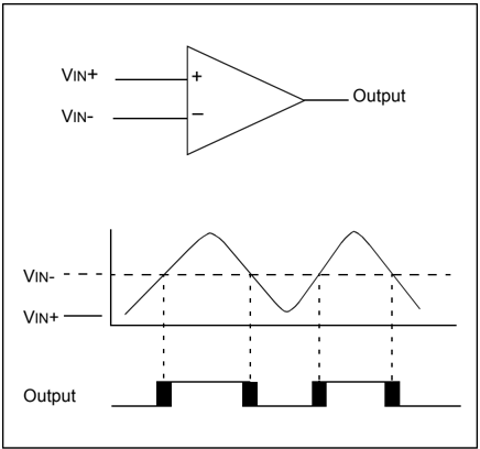
A single comparator is shown in Figure 22-2, along with the relationship between the analog input levels and the digital output. When the analog input at VIN+ is less than the analog input VIN-, the output of the comparator is a digital low level. When the analog input at VIN+ is greater than the analog input VIN-, the output of the comparator is a digital high level. The shaded areas of the output of the comparator in Figure 22-2 represent the uncertainty, due to input offsets and response time.
22.3 Comparator Reference
Depending on the comparator operating mode, either an external or internal voltage reference may be used. The analog signal present at VIN- is compared to the signal at VIN+ and the digital output of the comparator is adjusted accordingly (Figure 22-2).
FIGURE 22-2: SINGLE COMPARATOR
22.3.1 EXTERNAL REFERENCE SIGNAL
When external voltage references are used, the comparator module can be configured to have the comparators operate from the same or different reference sources. However, threshold detector applications may require the same reference. The reference signal must be between VSS and VDD and can be applied to either pin of the comparator(s).
22.3.2 INTERNAL REFERENCE SIGNAL
The comparator module also allows the selection of an internally generated voltage reference from the comparator voltage reference module. This module is described in more detail in Section 23.0 "Comparator Voltage Reference Module".
The internal reference is only available in the mode where four inputs are multiplexed to two comparators (CM2:CM0 = 110). In this mode, the internal voltage reference is applied to the VIN+ pin of both comparators.
22.4 Comparator Response Time
Response time is the minimum time, after selecting a new reference voltage or input source, before the comparator output has a valid level. If the internal reference is changed, the maximum delay of the internal voltage reference must be considered when using the comparator outputs. Otherwise, the maximum delay of the comparators should be used (see Section 28.0 "Electrical Characteristics").
22.5 Comparator Outputs
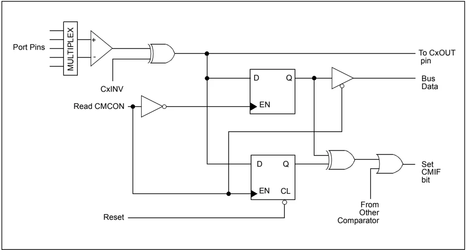
The comparator outputs are read through the CMCON register. These bits are read-only. The comparator outputs may also be directly output to the RA4 and RA5 I/O pins. When enabled, multiplexors in the output path of the RA4 and RA5 pins will switch and the output of each pin will be the unsynchronized output of the comparator. The uncertainty of each of the comparators is related to the input offset voltage and the response time given in the specifications. Figure 22-3 shows the comparator output block diagram.
The TRISA bits will still function as an output enable/disable for the RA4 and RA5 pins while in this mode.
The polarity of the comparator outputs can be changed using the C2INV and C1INV bits (CMCON<5:4>).
Note 1: When reading the PORT register, all pins configured as analog inputs will read as a '0'. Pins configured as digital inputs will convert an analog input according to the Schmitt Trigger input specification.
2: Analog levels on any pin defined as a digital input may cause the input buffer to consume more current than is specified.
FIGURE 22-3: COMPARATOR OUTPUT BLOCK DIAGRAM
22.6 Comparator Interrupts
The comparator interrupt flag is set whenever there is a change in the output value of either comparator. Software will need to maintain information about the status of the output bits, as read from CMCON<7:6>, to determine the actual change that occurred. The CMIF bit (PIR2<6>) is the Comparator Interrupt Flag. The CMIF bit must be reset by clearing it. Since it is also possible to write a '1' to this register, a simulated interrupt may be initiated.
Both the CMIE bit (PIE2<6>) and the PEIE bit (INTCON<6>) must be set to enable the interrupt. In addition, the GIE bit (INTCON<7>) must also be set. If any of these bits are clear, the interrupt is not enabled, though the CMIF bit will still be set if an interrupt condition occurs.
Note: If a change in the CMCON register (C1OUT or C2OUT) should occur when a read operation is being executed (start of the Q2 cycle), then the CMIF (PIR2<6>) interrupt flag may not get set.
The user, in the Interrupt Service Routine, can clear the interrupt in the following manner: a) Any read or write of CMCON will end the mismatch condition. b) Clear flag bit CMIF.
A mismatch condition will continue to set flag bit CMIF. Reading CMCON will end the mismatch condition and allow flag bit CMIF to be cleared.
22.7 Comparator Operation During Sleep
When a comparator is active and the device is placed in Sleep mode, the comparator remains active and the interrupt is functional if enabled. This interrupt will wake-up the device from Sleep mode, when enabled. Each operational comparator will consume additional current, as shown in the comparator specifications. To minimize power consumption while in Sleep mode, turn off the comparators (CM2:CM0 = 111) before entering Sleep. If the device wakes up from Sleep, the contents of the CMCON register are not affected.
22.8 Effects of a Reset
A device Reset forces the CMCON register to its Reset state, causing the comparator modules to be turned off (CM2:CM0 = 111). However, the input pins (RA0 through RA3) are configured as analog inputs by default on device Reset. The I/O configuration for these pins is determined by the setting of the PCFG3:PCFG0 bits (ADCON1<3:0>). Therefore, device current is minimized when analog inputs are present at Reset time.
DS39632E-page 278 © 2009 Microchip Technology Inc.
22.9 Analog Input Connection Considerations
A simplified circuit for an analog input is shown in Figure 22-4. Since the analog pins are connected to a digital output, they have reverse biased diodes to VDD and Vss. The analog input, therefore, must be between Vss and VDD. If the input voltage deviates from this range by more than 0.6V in either direction, one of the diodes is forward biased and a latch-up condition may occur. A maximum source impedance of 10 kΩ is recommended for the analog sources. Any external component connected to an analog input pin, such as a capacitor or a Zener diode, should have very little leakage current.
FIGURE 22-4: COMPARATOR ANALOG INPUT MODEL
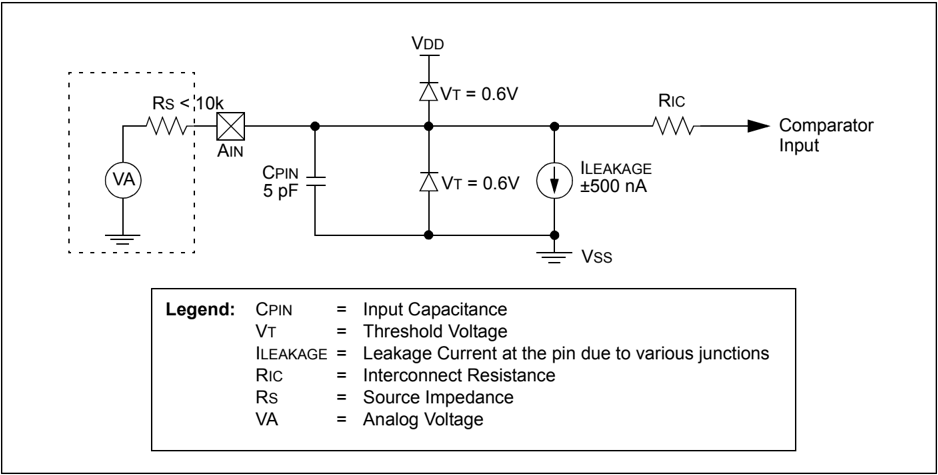
Legend: CPIN = Input Capacitance VT = Threshold Voltage ILEAKAGE = Leakage Current at the pin due to various junctions RIC = Interconnect Resistance Rs = Source Impedance VA = Analog Voltage
TABLE 22-1: REGISTERS ASSOCIATED WITH COMPARATOR MODULE
| Name | Bit 7 | Bit 6 | Bit 5 | Bit 4 | Bit 3 | Bit 2 | Bit 1 | Bit 0 | Reset Values on page |
|---|---|---|---|---|---|---|---|---|---|
| CMCON | C2OUT | C1OUT | C2INV | C1INV | CIS | CM2 | CM1 | CM0 | 55 |
| CVRCON | CVREN | CVROE | CVRR | CVRSS | CVR3 | CVR2 | CVR1 | CVR0 | 55 |
| INTCON | GIE/GIEH | PEIE/GIEL | TMR0IE | INT0IE | RBIE | TMR0IF | INT0IF | RBIF | 53 |
| PIR2 | OSCFIF | CMIF | USBIF | EEIF | BCLIF | HLVDIF | TMR3IF | CCP2IF | 56 |
| PIE2 | OSCFIE | CMIE | USBIE | EEIE | BCLIE | HLVDIE | TMR3IE | CCP2IE | 56 |
| IPR2 | OSCFIP | CMIP | USBIP | EEIP | BCLIP | HLVDIP | TMR3IP | CCP2IP | 56 |
| PORTA | — | RA6(1) | RA5 | RA4 | RA3 | RA2 | RA1 | RA0 | 56 |
| LATA | — | LATA6(1) | LATA5 | LATA4 | LATA3 | LATA2 | LATA1 | LATA0 | 56 |
| TRISA | — | TRISA6(1) | TRISA5 | TRISA4 | TRISA3 | TRISA2 | TRISA1 | TRISA0 | 56 |
Legend: — = unimplemented, read as ‘0’. Shaded cells are unused by the comparator module.
Note 1: PORTA<6> and its direction and latch bits are individually configured as port pins based on various oscillator modes. When disabled, these bits read as ‘0’.
NOTES:
23.0 COMPARATOR VOLTAGE REFERENCE MODULE
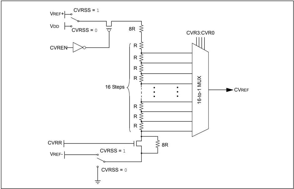
The comparator voltage reference is a 16-tap resistor ladder network that provides a selectable reference voltage. Although its primary purpose is to provide a reference for the analog comparators, it may also be used independently of them.
A block diagram of the module is shown in Figure 23-1. The resistor ladder is segmented to provide two ranges of CVREF values and has a power-down function to conserve power when the reference is not being used. The module’s supply reference can be provided from either device VDD/VSS or an external voltage reference.
23.1 Configuring the Comparator Voltage Reference
The voltage reference module is controlled through the CVRCON register (Register 23-1). The comparator voltage reference provides two ranges of output voltage, each with 16 distinct levels. The range to be used is selected by the CVRR bit (CVRCON<5>). The primary difference between the ranges is the size of the steps selected by the CVREF Selection bits (CVR3:CVR0), with one range offering finer resolution. The equations used to calculate the output of the comparator voltage reference are as follows:
If CVRR = 1:
CVREF = ((CVR3:CVR0)/24) x CVRSRC
If CVRR = 0:
CVREF = (CVRSRC/4) + (((CVR3:CVR0)/32) x CVRSRC)
The comparator reference supply voltage can come from either VDD and VSS, or the external VREF+ and VREF- that are multiplexed with RA2 and RA3. The voltage source is selected by the CVRSS bit (CVRCON<4>).
The settling time of the comparator voltage reference must be considered when changing the CVREF output (see Table 28-3 in Section 28.0 “Electrical Characteristics”).
REGISTER 23-1: CVRCON: COMPARATOR VOLTAGE REFERENCE CONTROL REGISTER
| R/W-0 | R/W-0 | R/W-0 | R/W-0 | R/W-0 | R/W-0 | R/W-0 | R/W-0 |
|---|---|---|---|---|---|---|---|
| CVREN | CVROE(1) | CVRR | CVRSS | CVR3 | CVR2 | CVR1 | CVR0 |
| bit 7 | bit 0 |
Legend:
R = Readable bit
W = Writable bit
U = Unimplemented bit, read as ‘0’
-n = Value at POR
‘1’ = Bit is set
‘0’ = Bit is cleared
x = Bit is unknown
bit 7
CVREN: Comparator Voltage Reference Enable bit
1 = CVREF circuit powered on
0 = CVREF circuit powered down
bit 6
CVROE: Comparator VREF Output Enable bit(1)
1 = CVREF voltage level is also output on the RA2/AN2/VREF-/CVREF pin
0 = CVREF voltage is disconnected from the RA2/AN2/VREF-/CVREF pin
bit 5
CVRR: Comparator VREF Range Selection bit
1 = 0 to 0.667 CVRSRC, with CVRSRC/24 step size (low range)
0 = 0.25 CVRSRC to 0.75 CVRSRC, with CVRSRC/32 step size (high range)
bit 4
CVRSS: Comparator VREF Source Selection bit
1 = Comparator reference source, CVRSRC = (VREF+) – (VREF-)
0 = Comparator reference source, CVRSRC = VDD – VSS
bit 3-0
CVR3:CVR0: Comparator VREF Value Selection bits (0 ≤ (CVR3:CVR0) ≤ 15)
When CVRR = 1:
CVREF = ((CVR3:CVR0)/24) • (CVRSRC)
When CVRR = 0:
CVREF = (CVRSRC/4) + ((CVR3:CVR0)/32) • (CVRSRC)
Note 1: CVROE overrides the TRISA<2> bit setting.
FIGURE 23-1: COMPARATOR VOLTAGE REFERENCE BLOCK DIAGRAM
23.2 Voltage Reference Accuracy/Error
The full range of voltage reference cannot be realized due to the construction of the module. The transistors on the top and bottom of the resistor ladder network (Figure 23-1) keep CVREF from approaching the reference source rails. The voltage reference is derived from the reference source; therefore, the CVREF output changes with fluctuations in that source. The tested absolute accuracy of the voltage reference can be found in Section 28.0 “Electrical Characteristics”.
23.3 Operation During Sleep
When the device wakes up from Sleep through an interrupt or a Watchdog Timer time-out, the contents of the CVRCON register are not affected. To minimize current consumption in Sleep mode, the voltage reference should be disabled.
23.4 Effects of a Reset
A device Reset disables the voltage reference by clearing bit, CVREN (CVRCON<7>). This Reset also disconnects the reference from the RA2 pin by clearing bit, CVROE (CVRCON<6>) and selects the high-voltage range by clearing bit, CVRR (CVRCON<5>). The CVR value select bits are also cleared.
23.5 Connection Considerations
The voltage reference module operates independently of the comparator module. The output of the reference generator may be connected to the RA2 pin if the TRISA<2> bit and the CVROE bit are both set. Enabling the voltage reference output onto RA2 when it is configured as a digital input will increase current consumption. Connecting RA2 as a digital output with CVRSS enabled will also increase current consumption.
The RA2 pin can be used as a simple D/A output with limited drive capability. Due to the limited current drive capability, a buffer must be used on the voltage reference output for external connections to VREF. Figure 23-2 shows an example buffering technique.
FIGURE 23-2: COMPARATOR VOLTAGE REFERENCE OUTPUT BUFFER EXAMPLE
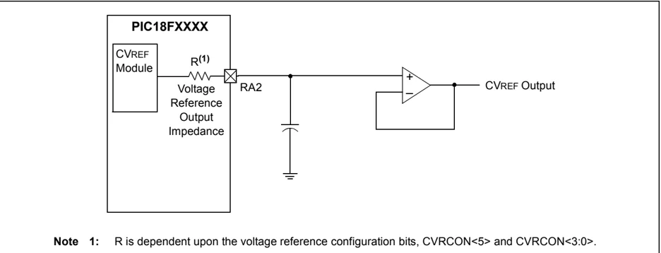
Note 1: R is dependent upon the voltage reference configuration bits, CVRCON<5> and CVRCON<3:0>.
TABLE 23-1: REGISTERS ASSOCIATED WITH COMPARATOR VOLTAGE REFERENCE
| Name | Bit 7 | Bit 6 | Bit 5 | Bit 4 | Bit 3 | Bit 2 | Bit 1 | Bit 0 | Reset Values on page |
|---|---|---|---|---|---|---|---|---|---|
| CVRCON | CVREN | CVROE | CVRR | CVRSS | CVR3 | CVR2 | CVR1 | CVR0 | 55 |
| CMCON | C2OUT | C1OUT | C2INV | C1INV | CIS | CM2 | CM1 | CM0 | 55 |
| TRISA | — | TRISA6(1) | TRISA5 | TRISA4 | TRISA3 | TRISA2 | TRISA1 | TRISA0 | 56 |
Legend: Shaded cells are not used with the comparator voltage reference.
Note 1: PORTA<6> and its direction and latch bits are individually configured as port pins based on various oscillator modes. When disabled, these bits read as ‘0’.
NOTES:
24.0 HIGH/LOW-VOLTAGE DETECT (HLVD)
PIC18F2455/2550/4455/4550 devices have a High/Low-Voltage Detect module (HLVD). This is a programmable circuit that allows the user to specify both a device voltage trip point and the direction of change from that point. If the device experiences an excursion past the trip point in that direction, an interrupt flag is set. If the interrupt is enabled, the program execution will branch to the interrupt vector address and the software can then respond to the interrupt.
The High/Low-Voltage Detect Control register (Register 24-1) completely controls the operation of the HLVD module. This allows the circuitry to be “turned off” by the user under software control which minimizes the current consumption for the device.
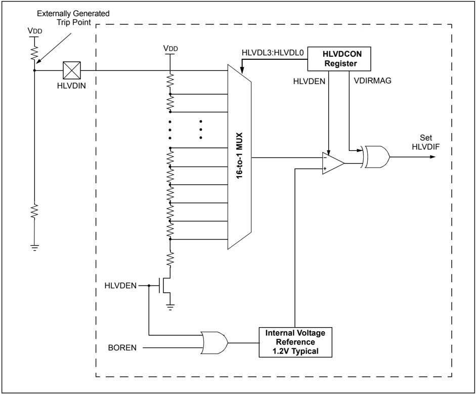
The block diagram for the HLVD module is shown in Figure 24-1.
REGISTER 24-1: HLVDCON: HIGH/LOW-VOLTAGE DETECT CONTROL REGISTER
| R/W-0 | U-0 | R-0 | R/W-0 | R/W-0 | R/W-1 | R/W-0 | R/W-1 |
|---|---|---|---|---|---|---|---|
| VDIRMAG | — | IRVST | HLVDEN | HLVDL3(1) | HLVDL2(1) | HLVDL1(1) | HLVDL0(1) |
| bit 7 | bit 0 |
Legend:
| R = Readable bit | W = Writable bit | U = Unimplemented bit, read as ‘0’ |
|---|---|---|
| -n = Value at POR | ‘1’ = Bit is set | ‘0’ = Bit is cleared |
| x = Bit is unknown |
bit 7 VDIRMAG: Voltage Direction Magnitude Select bit
1 = Event occurs when voltage equals or exceeds trip point (HLVDL3:HLVDL0)
0 = Event occurs when voltage equals or falls below trip point (HLVDL3:HLVDL0)
bit 6 Unimplemented: Read as ‘0’
bit 5 IRVST: Internal Reference Voltage Stable Flag bit
1 = Indicates that the voltage detect logic will generate the interrupt flag at the specified voltage range
0 = Indicates that the voltage detect logic will not generate the interrupt flag at the specified voltage range and the HLVD interrupt should not be enabled
bit 4 HLVDEN: High/Low-Voltage Detect Power Enable bit
1 = HLVD enabled
0 = HLVD disabled
bit 3-0 HLVDL3:HLVDL0: Voltage Detection Limit bits(1)
1111 = External analog input is used (input comes from the HLVDIN pin)
1110 = Maximum setting
.
.
.
0000 = Minimum setting
Note 1: See Table 28-6 in Section 28.0 “Electrical Characteristics” for specifications.
The module is enabled by setting the HLVDEN bit. Each time that the HLVD module is enabled, the circuitry requires some time to stabilize. The IRVST bit is a read-only bit and is used to indicate when the circuit is stable. The module can only generate an interrupt after the circuit is stable and IRVST is set.
The VDIRMAG bit determines the overall operation of the module. When VDIRMAG is cleared, the module monitors for drops in $V_{DD}$ below a predetermined set point. When the bit is set, the module monitors for rises in $V_{DD}$ above the set point.
24.1 Operation
When the HLVD module is enabled, a comparator uses an internally generated reference voltage as the set point. The set point is compared with the trip point, where each node in the resistor divider represents a trip point voltage. The "trip point" voltage is the voltage level at which the device detects a high or low-voltage event, depending on the configuration of the module. When the supply voltage is equal to the trip point, the voltage tapped off of the resistor array is equal to the internal reference voltage generated by the voltage reference module. The comparator then generates an interrupt signal by setting the HLVDF bit.
The trip point voltage is software programmable to any one of 16 values. The trip point is selected by programming the HLVDL3:HLVDL0 bits (HLVDCON<3:0>).
The HLVD module has an additional feature that allows the user to supply the trip voltage to the module from an external source. This mode is enabled when bits, HLVDL3:HLVDL0, are set to '1111'. In this state, the comparator input is multiplexed from the external input pin, HLV DIN. This gives users flexibility because it allows them to configure the High/Low-Voltage Detect interrupt to occur at any voltage in the valid operating range.
FIGURE 24-1: HLV D MODULE BLOCK DIAGRAM (WITH EXTERNAL INPUT)
24.2 HLVD Setup
The following steps are needed to set up the HLVD module:
- Disable the module by clearing the HLVDEN bit (HLVDCON<4>).
- Write the value to the HLVDL3:HLVDL0 bits that selects the desired HLVD trip point.
- Set the VDIRMAG bit to detect high voltage (VDIRMAG = 1) or low voltage (VDIRMAG = 0).
- Enable the HLVD module by setting the HLVDEN bit.
- Clear the HLVD Interrupt Flag, HLVDIF (PIR2<2>), which may have been set from a previous interrupt.
- Enable the HLVD interrupt, if interrupts are desired, by setting the HLVDIE and GIE/GIEH bits (PIE2<2> and INTCON<7>). An interrupt will not be generated until the IRVST bit is set.
24.3 Current Consumption
When the module is enabled, the HLVD comparator and voltage divider are enabled and will consume static current. The total current consumption, when enabled, is specified in electrical specification parameter D022 (Section 28.2 “DC Characteristics”).
Depending on the application, the HLVD module does not need to be operating constantly. To decrease the current requirements, the HLVD circuitry may only need to be enabled for short periods where the voltage is checked. After doing the check, the HLVD module may be disabled.
24.4 HLVD Start-up Time
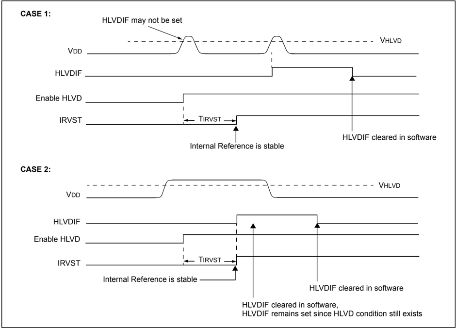
The internal reference voltage of the HLVD module, specified in electrical specification parameter D420 (see Table 28-6 in Section 28.0 “Electrical Characteristics”), may be used by other internal circuitry, such as the Programmable Brown-out Reset. If the HLVD or other circuits using the voltage reference are disabled to lower the device’s current consumption, the reference voltage circuit will require time to become stable before a low or high-voltage condition can be reliably detected. This start-up time, TIRVST, is an interval that is independent of device clock speed. It is specified in electrical specification parameter 36 (Table 28-12).
The HLVD interrupt flag is not enabled until TIRVST has expired and a stable reference voltage is reached. For this reason, brief excursions beyond the set point may not be detected during this interval. Refer to Figure 24-2 or Figure 24-3.
FIGURE 24-2: LOW-VOLTAGE DETECT OPERATION (VDIRMAG = 0)
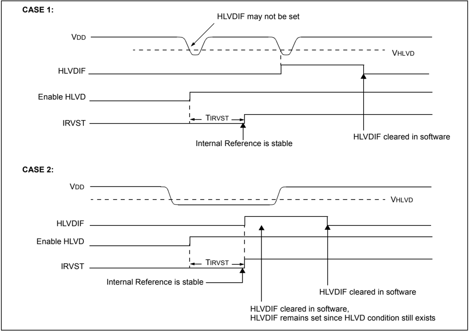
FIGURE 24-3: HIGH-VOLTAGE DETECT OPERATION (VDIRMAG = 1)
© 2009 Microchip Technology Inc.
24.5 Applications
In many applications, the ability to detect a drop below or rise above a particular threshold is desirable. For example, the HLVD module could be periodically enabled to detect Universal Serial Bus (USB) attach or detach. This assumes the device is powered by a lower voltage source than the USB when detached. An attach would indicate a high-voltage detect from, for example, 3.3V to 5V (the voltage on USB) and vice versa for a detach. This feature could save a design a few extra components and an attach signal (input pin).
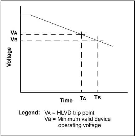
For general battery applications, Figure 24-4 shows a possible voltage curve. Over time, the device voltage decreases. When the device voltage reaches voltage, VA, the HLVD logic generates an interrupt at time, TA. The interrupt could cause the execution of an ISR, which would allow the application to perform "house-keeping tasks" and perform a controlled shutdown before the device voltage exits the valid operating range at TB. The HLVD, thus, would give the application a time window, represented by the difference between TA and TB, to safely exit.
FIGURE 24-4: TYPICAL HIGH/LOW-VOLTAGE DETECT APPLICATION
24.6 Operation During Sleep
When enabled, the HLVD circuitry continues to operate during Sleep. If the device voltage crosses the trip point, the HLVDIF bit will be set and the device will wake-up from Sleep. Device execution will continue from the interrupt vector address if interrupts have been globally enabled.
24.7 Effects of a Reset
A device Reset forces all registers to their Reset state. This forces the HLVD module to be turned off.
TABLE 24-1: REGISTERS ASSOCIATED WITH HIGH/LOW-VOLTAGE DETECT MODULE
| Name | Bit 7 | Bit 6 | Bit 5 | Bit 4 | Bit 3 | Bit 2 | Bit 1 | Bit 0 | Reset Values on page |
|---|---|---|---|---|---|---|---|---|---|
| HLVDCON | VDIRMAG | — | IRVST | HLVDEN | HLVDL3 | HLVDL2 | HLVDL1 | HLVDL0 | 54 |
| INTCON | GIE/GIEH | PEIE/GIEL | TMR0IE | INT0IE | RBIE | TMR0IF | INT0IF | RBIF | 53 |
| PIR2 | OSCFIF | CMIF | USBIF | EEIF | BCLIF | HLVDIF | TMR3IF | CCP2IF | 56 |
| PIE2 | OSCFIE | CMIE | USBIE | EEIE | BCLIE | HLVDIE | TMR3IE | CCP2IE | 56 |
| IPR2 | OSCFIP | CMIP | USBIP | EEIP | BCLIP | HLVDIP | TMR3IP | CCP2IP | 56 |
Legend: — = unimplemented, read as ‘0’. Shaded cells are unused by the HLVD module.
© 2009 Microchip Technology Inc. DS39632E-page 289