12.0 TIMER2/3 AND TIMER4/5
Note: This data sheet summarizes the features of this group of PIC24F devices. It is not intended to be a comprehensive reference source. For more information, refer to the “PIC24F Family Reference Manual”, “Timers” (DS39704).
The Timer2/3 and Timer4/5 modules are 32-bit timers, which can also be configured as four independent, 16-bit timers with selectable operating modes.
As a 32-bit timer, Timer2/3 and Timer4/5 operate in three modes:
- Two independent, 16-bit timers (Timer2 and Timer3) with all 16-bit operating modes (except Asynchronous Counter mode)
- Single 32-bit timer
- Single 32-bit synchronous counter
They also support these features:
- Timer gate operation
- Selectable prescaler settings
- Timer operation during Idle and Sleep modes
- Interrupt on a 32-Bit Period register match
- A/D Event Trigger (Timer2/3 only)
Individually, all four of the 16-bit timers can function as synchronous timers or counters. They also offer the features listed above, except for the A/D Event Trigger; this is implemented only with Timer3. The operating modes and enabled features are determined by setting the appropriate bit(s) in the T2CON, T3CON, T4CON and T5CON registers. T2CON and T4CON are shown in generic form in Register 12-1; T3CON and T5CON are shown in generic form in Register 12-2.
For 32-bit timer/counter operation, Timer2 and Timer4 are the least significant word; Timer3 and Timer4 are the most significant word of the 32-bit timers.
Note: For 32-bit operation, T3CON and T5CON control bits are ignored. Only T2CON and T4CON control bits are used for setup and control. Timer2 and Timer4 clock and gate inputs are utilized for the 32-bit timer modules, but an interrupt is generated with the Timer3 or Timer5 interrupt flags.
To configure Timer2/3 or Timer4/5 for 32-bit operation:
- Set the T32 bit (T2CON<3> or T4CON<3> = 1).
- Select the prescaler ratio for Timer2 or Timer4 using the TCKPS<1:0> bits.
- Set the Clock and Gating modes using the TCS and TGATE bits. If TCS is set to the external clock, RPINRx (TxCK) must be configured to an available RPn pin. See Section 10.4 “Peripheral Pin Select (PPS)” for more information.
- Load the timer period value. PR3 (or PR5) will contain the most significant word of the value while PR2 (or PR4) contains the least significant word.
- If interrupts are required, set the Timer3/5 Interrupt Enable bit, T3IE or T5IE; use the priority bits, T3IP<2:0> or T5IP<2:0>, to set the interrupt priority. Note that while Timer2 or Timer4 controls the timer, the interrupt appears as a Timer3 or Timer5 interrupt.
- Set the TON bit (= 1).
The timer value, at any point, is stored in the register pair, TMR3:TMR2 (or TMR5:TMR4). TMR3 (TMR5) always contains the most significant word of the count, while TMR2 (TMR4) contains the least significant word.
To configure any of the timers for individual 16-bit operation:
- Clear the T32 bit corresponding to that timer (T2CON<3> for Timer2 and Timer3 or T4CON<3> for Timer4 and Timer5).
- Select the timer prescaler ratio using the TCKPS<1:0> bits.
- Set the Clock and Gating modes using the TCS and TGATE bits. See Section 10.4 “Peripheral Pin Select (PPS)” for more information.
- Load the timer period value into the PRx register.
- If interrupts are required, set the Timerx Interrupt Enable bit, TxIE; use the priority bits, TxIP<2:0>, to set the interrupt priority.
- Set the TON bit (TxCON<15> = 1).
FIGURE 12-1: TIMER2/3 AND TIMER4/5 (32-BIT) BLOCK DIAGRAM
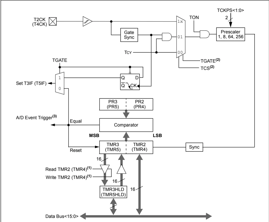
Note 1: The 32-Bit Timer Configuration bit, T32, must be set for 32-bit timer/counter operation. All control bits are respective to the T2CON and T4CON registers. 2: This peripheral’s inputs must be assigned to an available RPn pin before use. Please see Section 10.4 “Peripheral Pin Select (PPS)” for more information. 3: The A/D Event Trigger is available only on Timer2/3.
DS39881E-page 128 © 2010-2013 Microchip Technology Inc.
FIGURE 12-2: TIMER2 AND TIMER4 (16-BIT SYNCHRONOUS) BLOCK DIAGRAM
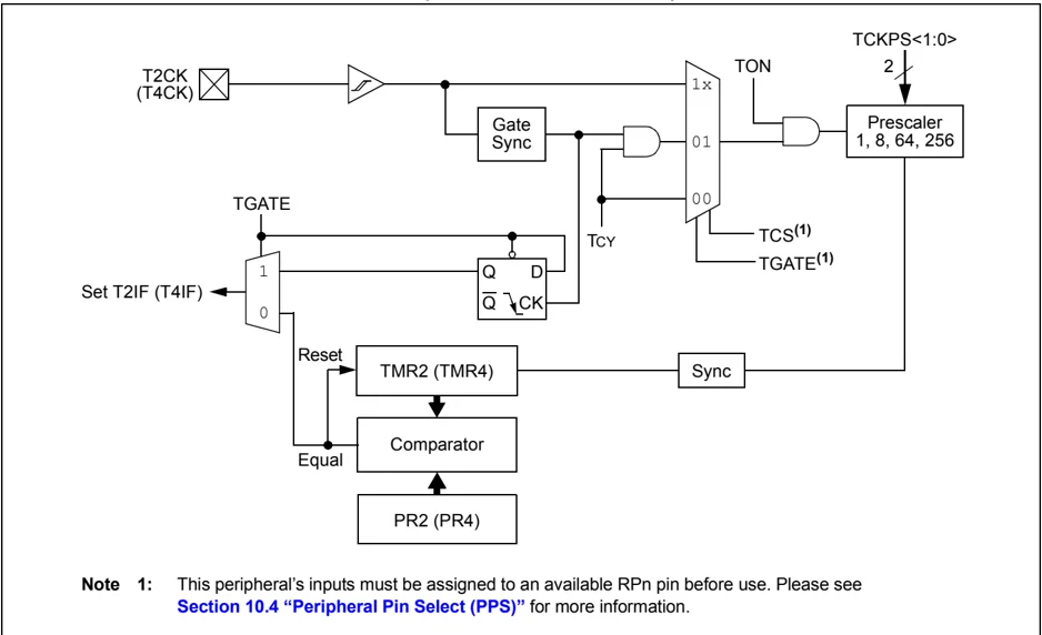
Note 1: This peripheral’s inputs must be assigned to an available RPn pin before use. Please see Section 10.4 “Peripheral Pin Select (PPS)” for more information.
FIGURE 12-3: TIMER3 AND TIMER5 (16-BIT SYNCHRONOUS) BLOCK DIAGRAM
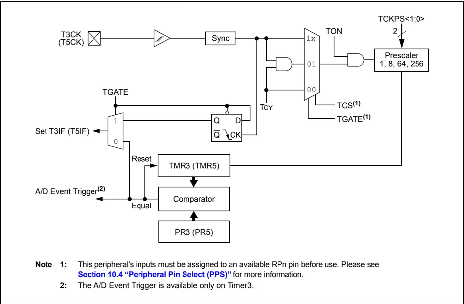
Note 1: This peripheral’s inputs must be assigned to an available RPn pin before use. Please see Section 10.4 “Peripheral Pin Select (PPS)” for more information. 2: The A/D Event Trigger is available only on Timer3.
REGISTER 12-1: TxCON: TIMER2 AND TIMER4 CONTROL REGISTER
| R/W-0 | U-0 | R/W-0 | U-0 | U-0 | U-0 | U-0 | U-0 |
|---|---|---|---|---|---|---|---|
| TON | — | TSIDL | — | — | — | — | — |
| bit 15 | bit 8 |
| U-0 | R/W-0 | R/W-0 | R/W-0 | R/W-0 | U-0 | R/W-0 | U-0 |
|---|---|---|---|---|---|---|---|
| — | TGATE | TCKPS1 | TCKPS0 | T32(1) | — | TCS(2) | — |
| bit 7 | bit 0 |
Legend:
R = Readable bit
W = Writable bit
U = Unimplemented bit, read as ‘0’
-n = Value at POR
‘1’ = Bit is set
‘0’ = Bit is cleared
x = Bit is unknown
bit 15
TON: Timerx On bit
When TxCON<3> = 1:
1 = Starts 32-bit Timerx/y
0 = Stops 32-bit Timerx/y
When TxCON<3> = 0:
1 = Starts 16-bit Timerx
0 = Stops 16-bit Timerx
bit 14
Unimplemented: Read as ‘0’
bit 13
TSIDL: Timerx Stop in Idle Mode bit
1 = Discontinues module operation when device enters Idle mode
0 = Continues module operation in Idle mode
bit 12-7
Unimplemented: Read as ‘0’
bit 6
TGATE: Timerx Gated Time Accumulation Enable bit
When TCS = 1:
This bit is ignored.
When TCS = 0:
1 = Gated time accumulation is enabled
0 = Gated time accumulation is disabled
bit 5-4
TCKPS<1:0>: Timerx Input Clock Prescale Select bits
11 = 1:256
10 = 1:64
01 = 1:8
00 = 1:1
bit 3
T32: 32-Bit Timer Mode Select bit(1)
1 = Timerx and Timery form a single 32-bit timer
0 = Timerx and Timery act as two 16-bit timers
In 32-bit mode, T3CON control bits do not affect 32-bit timer operation.
bit 2
Unimplemented: Read as ‘0’
bit 1
TCS: Timerx Clock Source Select bit(2)
1 = External clock from pin, TxCK (on the rising edge)
0 = Internal clock (Fosc/2)
bit 0
Unimplemented: Read as ‘0’
Note 1: In 32-bit mode, the T3CON or T5CON control bits do not affect 32-bit timer operation.
2: If TCS = 1, RPINRx (TxCK) must be configured to an available RPn pin. For more information, see Section 10.4 “Peripheral Pin Select (PPS)”.
REGISTER 12-2: TyCON: TIMER3 AND TIMER5 CONTROL REGISTER
| R/W-0 | U-0 | R/W-0 | U-0 | U-0 | U-0 | U-0 | U-0 |
|---|---|---|---|---|---|---|---|
| TON⁽¹⁾ | — | TSIDL⁽¹⁾ | — | — | — | — | — |
| bit 15 | bit 8 |
| U-0 | R/W-0 | R/W-0 | R/W-0 | U-0 | U-0 | R/W-0 | U-0 |
|---|---|---|---|---|---|---|---|
| — | TGATE⁽¹⁾ | TCKPS1⁽¹⁾ | TCKPS0⁽¹⁾ | — | — | TCS⁽¹,²⁾ | — |
| bit 7 | bit 0 |
Legend:
R = Readable bit
W = Writable bit
U = Unimplemented bit, read as ‘0’
-n = Value at POR
‘1’ = Bit is set
‘0’ = Bit is cleared
x = Bit is unknown
bit 15
TON: Timery On bit⁽¹⁾
1 = Starts 16-bit Timery
0 = Stops 16-bit Timery
bit 14
Unimplemented: Read as ‘0’
bit 13
TSIDL: Timery Stop in Idle Mode bit⁽¹⁾
1 = Discontinues module operation when device enters Idle mode
0 = Continues module operation in Idle mode
bit 12-7
Unimplemented: Read as ‘0’
bit 6
TGATE: Timery Gated Time Accumulation Enable bit⁽¹⁾
When TCS = 1:
This bit is ignored.
When TCS = 0:
1 = Gated time accumulation is enabled
0 = Gated time accumulation is disabled
bit 5-4
TCKPS<1:0>: Timery Input Clock Prescale Select bits⁽¹⁾
11 = 1:256
10 = 1:64
01 = 1:8
00 = 1:1
bit 3-2
Unimplemented: Read as ‘0’
bit 1
TCS: Timery Clock Source Select bit⁽¹,²⁾
1 = External clock from pin, TyCK (on the rising edge)
0 = Internal clock (Fosc/2)
bit 0
Unimplemented: Read as ‘0’
Note 1: When 32-bit operation is enabled (T2CON<3> or T4CON<3> = 1), these bits have no effect on Timery operation; all timer functions are set through T2CON and T4CON.
2: If TCS = 1, RPINRx (TxCK) must be configured to an available RPn pin. See Section 10.4 “Peripheral Pin Select (PPS)” for more information.
NOTES:
13.0 INPUT CAPTURE
Note: This data sheet summarizes the features of this group of PIC24F devices. It is not intended to be a comprehensive reference source. For more information, refer to the “PIC24F Family Reference Manual”, “Input Capture” (DS39701).
FIGURE 13-1: INPUT CAPTURE x BLOCK DIAGRAM
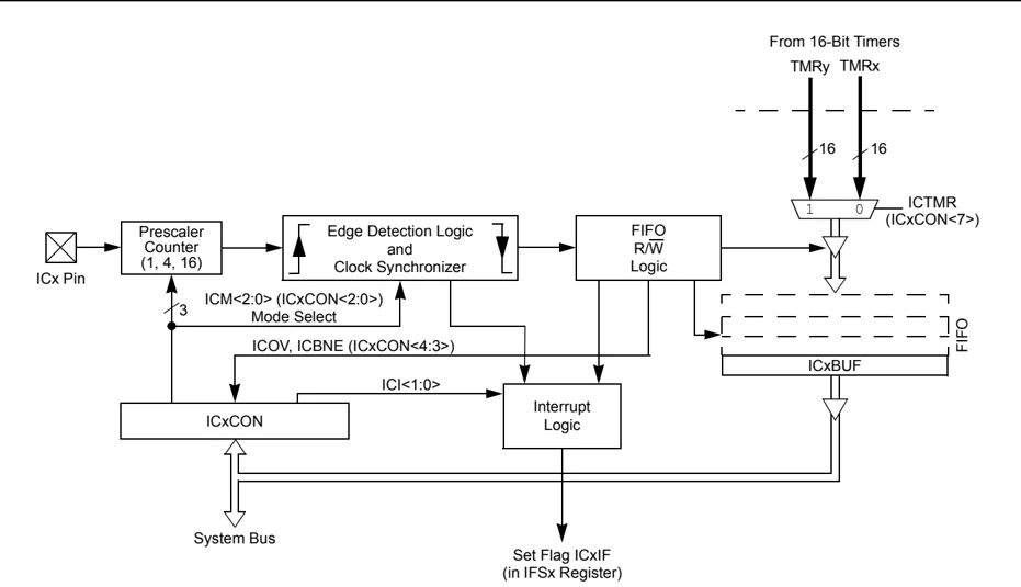
Note 1: An ‘x’ in a signal, register or bit name denotes the number of the capture channel. 2: This peripheral’s inputs must be assigned to an available RPn pin before use. Please see Section 10.4 “Peripheral Pin Select (PPS)” for more information.
13.1 Input Capture Registers
REGISTER 13-1: ICxCON: INPUT CAPTURE x CONTROL REGISTER
| U-0 | U-0 | R/W-0 | U-0 | U-0 | U-0 | U-0 | U-0 |
|---|---|---|---|---|---|---|---|
| — | — | ICSIDL | — | — | — | — | — |
| bit 15 | bit 8 |
| R/W-0 | R/W-0 | R/W-0 | R-0, HC | R-0, HC | R/W-0 | R/W-0 | R/W-0 |
|---|---|---|---|---|---|---|---|
| ICTMR | ICI1 | ICI0 | ICOV | ICBNE | ICM2⁽¹⁾ | ICM1⁽¹⁾ | ICM0⁽¹⁾ |
| bit 7 | bit 0 |
Legend:
- R = Readable bit
- W = Writable bit
- U = Unimplemented bit, read as ‘0’
- -n = Value at POR
- ‘1’ = Bit is set
- ‘0’ = Bit is cleared
- x = Bit is unknown
- HC = Hardware Clearable bit
bit 15-14 Unimplemented: Read as ‘0’
bit 13 ICSIDL: Input Capture x Stop in Idle Control bit
- 1 = Input capture module will halt in CPU Idle mode
- 0 = Input capture module will continue to operate in CPU Idle mode
bit 12-8 Unimplemented: Read as ‘0’
bit 7 ICTMR: Input Capture x Timer Select bit
- 1 = TMR2 contents are captured on capture event
- 0 = TMR3 contents are captured on capture event
bit 6-5 ICI<1:0>: Select Number of Captures per Interrupt bits
- 11 = Interrupt on every fourth capture event
- 10 = Interrupt on every third capture event
- 01 = Interrupt on every second capture event
- 00 = Interrupt on every capture event
bit 4 ICOV: Input Capture x Overflow Status Flag bit (read-only)
- 1 = Input capture overflow occurred
- 0 = No input capture overflow occurred
bit 3 ICBNE: Input Capture x Buffer Empty Status bit (read-only)
- 1 = Input capture buffer is not empty, at least one more capture value can be read
- 0 = Input capture buffer is empty
bit 2-0 ICM<2:0>: Input Capture x Mode Select bits⁽¹⁾
- 111 = Input capture functions as interrupt pin only when device is in Sleep or Idle mode (rising edge detect only, all other control bits are not applicable)
- 110 = Unused (module is disabled)
- 101 = Capture mode, every 16th rising edge
- 100 = Capture mode, every 4th rising edge
- 011 = Capture mode, every rising edge
- 010 = Capture mode, every falling edge
- 001 = Capture mode, every edge (rising and falling) – ICI<1:0> bits do not control interrupt generation for this mode
- 000 = Input capture module is turned off
Note 1: RPINRx (ICxRx) must be configured to an available RPn pin. For more information, see Section 10.4 “Peripheral Pin Select (PPS)”.
14.0 OUTPUT COMPARE
Note: This data sheet summarizes the features of this group of PIC24F devices. It is not intended to be a comprehensive reference source. For more information, refer to the "PIC24F Family Reference Manual", "Output Compare" (DS39706).
14.1 Setup for Single Output Pulse Generation
When the OCM<2:0> control bits (OCxCON<2:0>) are set to '100', the selected output compare channel initializes the OCx pin to the low state and generates a single output pulse.
To generate a single output pulse, the following steps are required (these steps assume the timer source is initially turned off, but this is not a requirement for the module operation):
- Determine the instruction clock cycle time. Take into account the frequency of the external clock to the timer source (if one is used) and the timer prescaler settings.
- Calculate the time to the rising edge of the output pulse relative to the TMRy start value (0000h).
- Calculate the time to the falling edge of the pulse based on the desired pulse width and the time to the rising edge of the pulse.
- Write the values computed in Steps 2 and 3 above into the Output Compare x register, OCxR, and the Output Compare x Secondary register, OCxRS, respectively.
- Set the Timery Period register, PRy, to a value equal to or greater than the value in OCxRS, the Output Compare x Secondary register.
- Set the OCMx bits to '100' and the OCTSEL (OCxCON<3>) bit to the desired timer source. The OCx pin state will now be driven low.
- Set the TON (TyCON<15>) bit to '1', which enables the compare time base to count.
- Upon the first match between TMRy and OCxR, the OCx pin will be driven high.
- When the incrementing timer, TMRy, matches the Output Compare x Secondary register, OCxRS, the second and trailing edge (high-to-low) of the pulse is driven onto the OCx pin. No additional pulses are driven onto the OCx pin and it remains at low. As a result of the second compare match event, the OCxIF interrupt flag bit is set, which will result in an interrupt if it is enabled, by setting the OCxIE bit. For further information on peripheral interrupts, refer to Section 7.0 "Interrupt Controller".
- To initiate another single pulse output, change the Timer and Compare register settings, if needed, and then issue a write to set the OCMx bits to '100'. Disabling and re-enabling the timer and clearing the TMRy register are not required, but may be advantageous for defining a pulse from a known event time boundary.
The output compare module does not have to be disabled after the falling edge of the output pulse. Another pulse can be initiated by rewriting the value of the OCxCON register.
14.2 Setup for Continuous Output Pulse Generation
When the OCM<2:0> control bits (OCxCON<2:0>) are set to '101', the selected output compare channel initializes the OCx pin to the low state and generates output pulses on each and every compare match event.
For the user to configure the module for the generation of a continuous stream of output pulses, the following steps are required (these steps assume the timer source is initially turned off, but this is not a requirement for the module operation):
- Determine the instruction clock cycle time. Take into account the frequency of the external clock to the timer source (if one is used) and the timer prescaler settings.
- Calculate the time to the rising edge of the output pulse relative to the TMRy start value (0000h).
- Calculate the time to the falling edge of the pulse based on the desired pulse width and the time to the rising edge of the pulse.
- Write the values computed in Steps 2 and 3 above into the Output Compare x register, OCxR, and the Output Compare x Secondary register, OCxRS, respectively.
- Set the Timery Period register, PRy, to a value equal to or greater than the value in OCxRS.
- Set the OCMx bits to '101' and the OCTSEL bit to the desired timer source. The OCx pin state will now be driven low.
- Enable the compare time base by setting the TON (TyCON<15>) bit to '1'.
- Upon the first match between TMRy and OCxR, the OCx pin will be driven high.
- When the compare time base, TMRy, matches the OCxRS, the second and trailing edge (high-to-low) of the pulse is driven onto the OCx pin.
- As a result of the second compare match event, the OCxIF interrupt flag bit set.
- When the compare time base and the value in its respective Timery Period register match, the TMRy register resets to 0x0000 and resumes counting.
- Steps 8 through 11 are repeated and a continuous stream of pulses is generated indefinitely. The OCxIF flag is set on each OCxRS/TMRy compare match event.
14.3 Pulse-Width Modulation Mode
Note: This peripheral contains input and output functions that may need to be configured by the Peripheral Pin Select. See Section 10.4 “Peripheral Pin Select (PPS)” for more information.
The following steps should be taken when configuring the output compare module for PWM operation:
- Set the PWM period by writing to the selected Timery Period register (PRy).
- Set the PWM duty cycle by writing to the OCxRS register.
- Write the OCxR register with the initial duty cycle.
- Enable interrupts, if required, for the timer and output compare modules. The output compare interrupt is required for PWM Fault pin utilization.
- Configure the output compare module for one of two PWM Operation modes by writing to the Output Compare Mode bits, OCM<2:0> (OCxCON<2:0>).
- Set the TMRy prescale value and enable the time base by setting TON (TyCON<15>) = 1.
Note: The OCxR register should be initialized before the output compare module is first enabled. The OCxR register becomes a read-only Duty Cycle register when the module is operated in the PWM modes. The value held in OCxR will become the PWM duty cycle for the first PWM period. The contents of the Output Compare x Secondary register, OCxRS, will not be transferred into OCxR until a time base period match occurs.
14.3.1 PWM PERIOD
The PWM period is specified by writing to PRy, the Timery Period register. The PWM period can be calculated using Equation 14-1.
EQUATION 14-1: CALCULATING THE PWM PERIOD(1)
PWM Period = [(PRy) + 1] • TCY • (Timer Prescale Value)
Where: PWM Frequency = 1/[PWM Period]
Note 1: Based on TCY = 2 * TOSC; Doze mode and PLL are disabled.
Note: A PRy value of N will produce a PWM period of N + 1 time base count cycles. For example, a value of 7 written into the PRy register will yield a period consisting of 8 time base cycles.
14.3.2 PWM DUTY CYCLE
The PWM duty cycle is specified by writing to the OCxRS register. The OCxRS register can be written to at any time, but the duty cycle value is not latched into OCxR until a match between PRy and TMRy occurs (i.e., the period is complete). This provides a double buffer for the PWM duty cycle and is essential for glitchless PWM operation. In the PWM mode, OCxR is a read-only register.
Some important boundary parameters of the PWM duty cycle include:
- If the Output Compare x register, OCxR, is loaded with 0000h, the OCx pin will remain low (0% duty cycle).
- If OCxR is greater than PRy (Timery Period register), the pin will remain high (100% duty cycle).
- If OCxR is equal to PRy, the OCx pin will be low for one time base count value and high for all other count values.
See Example 14-1 for PWM mode timing details. Table 14-1 and Table 14-2 show example PWM frequencies and resolutions for a device operating at 4 and 16 MIPS.
EQUATION 14-2: CALCULATION FOR MAXIMUM PWM RESOLUTION(1)
$ Maximum PWM Resolution (bits) = \frac\log_10\left(\fracFCYF_PWM \cdot (Timer Prescale Value)\right)\log_10(2) bits $
Note 1: Based on FCY = FOSC/2; Doze mode and PLL are disabled.
DS39881E-page 136 © 2010-2013 Microchip Technology Inc.
EXAMPLE 14-1: PWM PERIOD AND DUTY CYCLE CALCULATIONS(1)
-
Find the Timer Period register value for a desired PWM frequency of 52.08 kHz, where FOSC = 8 MHz with PLL (32 MHz device clock rate) and a Timer2 prescaler setting of 1:1. TCY = 2 • TOSC = 62.5 ns PWM Period = 1/PWM Frequency = 1/52.08 kHz = 19.2 µs PWM Period = (PR2 + 1) • TCY • (Timer2 Prescale Value) 19.2 µs = (PR2 + 1) • 62.5 ns • 1 PR2 = 306
-
Find the maximum resolution of the duty cycle that can be used with a 52.08 kHz frequency and a 32 MHz device clock rate: PWM Resolution = log₁₀(FCY/FPWM)/log₁₀2) bits = (log₁₀(16 MHz/52.08 kHz)/log₁₀2) bits = 8.3 bits
Note 1: Based on TCY = 2 * TOSC; Doze mode and PLL are disabled.
TABLE 14-1: EXAMPLE PWM FREQUENCIES AND RESOLUTIONS AT 4 MIPS (FCY = 4 MHz)(1)
| PWM Frequency | 7.6 Hz | 61 Hz | 122 Hz | 977 Hz | 3.9 kHz | 31.3 kHz | 125 kHz |
|---|---|---|---|---|---|---|---|
| Timer Prescaler Ratio | 8 | 1 | 1 | 1 | 1 | 1 | 1 |
| Period Register Value | FFFFh | FFFFh | 7FFFh | 0FFFh | 03FFh | 007Fh | 001Fh |
| Resolution (bits) | 16 | 16 | 15 | 12 | 10 | 7 | 5 |
Note 1: Based on FCY = FOSC/2; Doze mode and PLL are disabled.
TABLE 14-2: EXAMPLE PWM FREQUENCIES AND RESOLUTIONS AT 16 MIPS (FCY = 16 MHz)(1)
| PWM Frequency | 30.5 Hz | 244 Hz | 488 Hz | 3.9 kHz | 15.6 kHz | 125 kHz | 500 kHz |
|---|---|---|---|---|---|---|---|
| Timer Prescaler Ratio | 8 | 1 | 1 | 1 | 1 | 1 | 1 |
| Period Register Value | FFFFh | FFFFh | 7FFFh | 0FFFh | 03FFh | 007Fh | 001Fh |
| Resolution (bits) | 16 | 16 | 15 | 12 | 10 | 7 | 5 |
Note 1: Based on FCY = FOSC/2; Doze mode and PLL are disabled.
FIGURE 14-1: OUTPUT COMPARE x MODULE BLOCK DIAGRAM
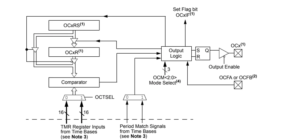
Note 1: Where 'x' is shown, reference is made to the registers associated with the respective Output Compare Channels 1 through 5. 2: The OCFA pin controls the OC1-OC4 channels. The OCFB pin controls the OC5 channel. 3: Each output compare channel can use one of two selectable time bases. Refer to the device data sheet for the time bases associated with the module. 4: This peripheral's inputs and outputs must be assigned to an available RPn pin before use. Please see Section 10.4 “Peripheral Pin Select (PPS)” for more information.
DS39881E-page 138 © 2010-2013 Microchip Technology Inc.
14.4 Output Compare Register
REGISTER 14-1: OCxCON: OUTPUT COMPARE x CONTROL REGISTER
| U-0 | U-0 | R/W-0 | U-0 | U-0 | U-0 | U-0 | U-0 |
|---|---|---|---|---|---|---|---|
| — | — | OCSIDL | — | — | — | — | — |
| bit 15 bit 8 |
| U-0 | U-0 | U-0 | R-0, HC | R/W-0 | R/W-0 | R/W-0 | R/W-0 |
|---|---|---|---|---|---|---|---|
| — | — | — | OCFLT | OCTSEL | OCM2(1) | OCM1(1) | OCM0(1) |
| bit 7 bit 0 |
Legend:
- R = Readable bit
- W = Writable bit
- U = Unimplemented bit, read as ‘0’
- -n = Value at POR
- ‘1’ = Bit is set
- ‘0’ = Bit is cleared
- x = Bit is unknown
- HC = Hardware Clearable bit
bit 15-14 Unimplemented: Read as ‘0’
bit 13 OCSIDL: Output Compare x Stop in Idle Mode Control bit
- 1 = Output Compare x halts in CPU Idle mode
- 0 = Output Compare x continues to operate in CPU Idle mode
bit 12-5 Unimplemented: Read as ‘0’
bit 4 OCFLT: PWM Fault Condition Status bit
- 1 = PWM Fault condition has occurred (cleared in HW only)
- 0 = No PWM Fault condition has occurred (this bit is only used when OCM<2:0> = 111)
bit 3 OCTSEL: Output Compare x Timer Select bit
- 1 = Timer3 is the clock source for Output Compare x
- 0 = Timer2 is the clock source for Output Compare x Refer to the device data sheet for specific time bases available to the output compare module.
bit 2-0 OCM<2:0>: Output Compare x Mode Select bits(1)
- 111 = PWM mode on OCx; Fault pin, OCFA, is enabled(2)
- 110 = PWM mode on OCx; Fault pin, OCFA, is disabled(2)
- 101 = Initializes OCx pin low, generates continuous output pulses on OCx pin
- 100 = Initializes OCx pin low, generates single output pulse on OCx pin
- 011 = Compare event toggles OCx pin
- 010 = Initializes OCx pin high, compare event forces OCx pin low
- 001 = Initializes OCx pin low, compare event forces OCx pin high
- 000 = Output compare channel is disabled
Note 1: RPORx (OCx) must be configured to an available RPn pin. For more information, see Section 10.4 “Peripheral Pin Select (PPS)”.
2: The OCFA pin controls the OC1-OC4 channels. The OCFB pin controls the OC5 channel.
NOTES:
15.0 SERIAL PERIPHERAL INTERFACE (SPI)
Note: This data sheet summarizes the features of this group of PIC24F devices. It is not intended to be a comprehensive reference source. For more information, refer to the “PIC24F Family Reference Manual”, “Serial Peripheral Interface (SPI)” (DS39699)
The Serial Peripheral Interface (SPI) module is a synchronous serial interface useful for communicating with other peripheral or microcontroller devices. These peripheral devices may be serial EEPROMs, shift registers, display drivers, A/D Converters, etc. The SPI module is compatible with the SPI and SIOP Motorola® interfaces.
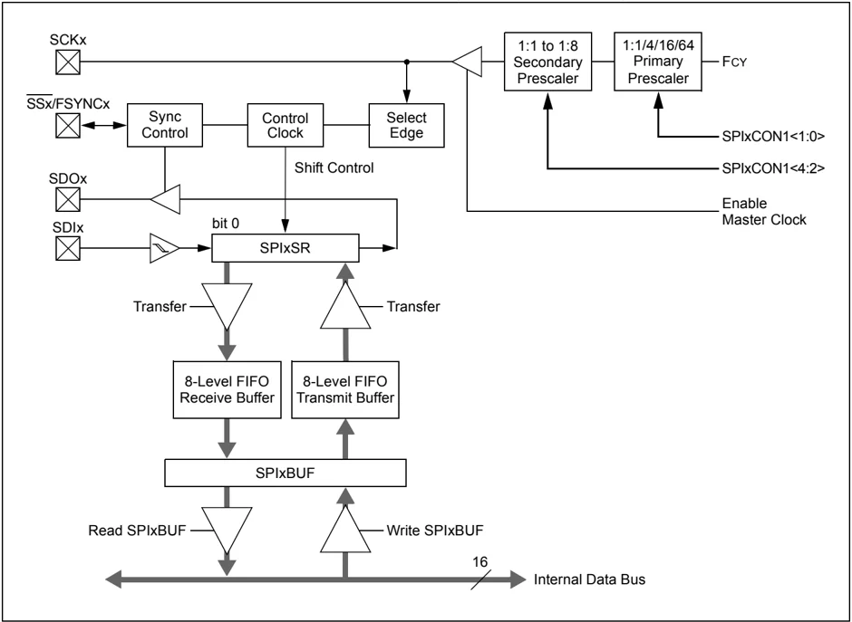
The module supports operation in two buffer modes. In Standard mode, data is shifted through a single serial buffer. In Enhanced Buffer mode, data is shifted through an 8-level FIFO buffer.
Note: Do not perform read-modify-write operations (such as bit-oriented instructions) on the SPIxBUF register in either Standard or Enhanced Buffer mode.
The module also supports a basic framed SPI protocol while operating in either Master or Slave mode. A total of four framed SPI configurations are supported.
The SPI serial interface consists of four pins:
- SDIx: Serial Data Input
- SDOx: Serial Data Output
- SCKx: Shift Clock Input or Output
- SSx: Active-Low Slave Select or Frame Synchronization I/O Pulse
The SPI module can be configured to operate using 2, 3 or 4 pins. In the 3-pin mode, SSx is not used. In the 2-pin mode, both SDOx and SSx are not used.
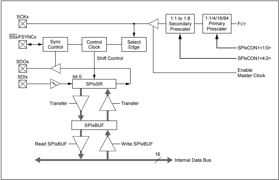
Block diagrams of the module in Standard and Enhanced modes are shown in Figure 15-1 and Figure 15-2.
Depending on the pin count, PIC24FJ64GA004 family devices offer one or two SPI modules on a single device.
Note: In this section, the SPI modules are referred to together as SPIx or separately as SPI1 and SPI2. Special Function Registers will follow a similar notation. For example, SPIxCON1 or SPIxCON2 refers to the control register for the SPI1 or SPI2 module.
To set up the SPIx module for the Standard Master mode of operation:
- If using interrupts: a) Clear the SPIxIF bit in the respective IFSx register. b) Set the SPIxIE bit in the respective IECx register. c) Write the SPIxIP bits in the respective IPCx register to set the interrupt priority.
- Write the desired settings to the SPIxCON1 and SPIxCON2 registers with the MSTEN bit (SPIxCON1<5>) = 1.
- Clear the SPIROV bit (SPIxSTAT<6>).
- Enable SPIx operation by setting the SPIEN bit (SPIxSTAT<15>).
- Write the data to be transmitted to the SPIxBUF register. Transmission (and reception) will start as soon as data is written to the SPIxBUF register.
To set up the SPIx module for the Standard Slave mode of operation:
- Clear the SPIxBUF register.
- If using interrupts: a) Clear the SPIxIF bit in the respective IFSx register. b) Set the SPIxIE bit in the respective IECx register. c) Write the SPIxIP bits in the respective IPCx register to set the interrupt priority.
- Write the desired settings to the SPIxCON1 and SPIxCON2 registers with the MSTEN bit (SPIxCON1<5>) = 0.
- Clear the SMP bit (SPIxCON1<9>).
- If the CKE bit is set, then the SSEN bit (SPIxCON1<7>) must be set to enable the SSx pin.
- Clear the SPIROV bit (SPIxSTAT<6>).
- Enable SPIx operation by setting the SPIEN bit (SPIxSTAT<15>).
FIGURE 15-1: SPIx MODULE BLOCK DIAGRAM (STANDARD MODE)
To set up the SPIx module for the Enhanced Buffer Master mode of operation:
- If using interrupts: a) Clear the SPIxIF bit in the respective IFSx register. b) Set the SPIxIE bit in the respective IECx register. c) Write the SPIxIP bits in the respective IPCx register.
- Write the desired settings to the SPIxCON1 and SPIxCON2 registers with the MSTEN bit (SPIxCON1<5>) = 1.
- Clear the SPIROV bit (SPIxSTAT<6>).
- Select Enhanced Buffer mode by setting the SPIBEN bit (SPIxCON2<0>).
- Enable SPIx operation by setting the SPIEN bit (SPIxSTAT<15>).
- Write the data to be transmitted to the SPIxBUF register. Transmission (and reception) will start as soon as data is written to the SPIxBUF register.
To set up the SPIx module for the Enhanced Buffer Slave mode of operation:
- Clear the SPIxBUF register.
- If using interrupts:
- Clear the SPIxIF bit in the respective IFSx register.
- Set the SPIxIE bit in the respective IECx register.
- Write the SPIxIP bits in the respective IPCx register to set the interrupt priority.
- Write the desired settings to the SPIxCON1 and SPIxCON2 registers with the MSTEN bit (SPIxCON1<5>) = 0.
- Clear the SMP bit.
- If the CKE bit is set, then the SSEN bit must be set, thus enabling the \overlineSSx pin.
- Clear the SPIROV bit (SPIxSTAT<6>).
- Select Enhanced Buffer mode by setting the SPIBEN bit (SPIxCON2<0>).
- Enable SPIx operation by setting the SPIEN bit (SPIxSTAT<15>).
FIGURE 15-2: SPIx MODULE BLOCK DIAGRAM (ENHANCED MODE)
REGISTER 15-1: SPIxSTAT: SPIx STATUS AND CONTROL REGISTER
| R/W-0 | U-0 | R/W-0 | U-0 | U-0 | R-0 | R-0 | R-0 |
|---|---|---|---|---|---|---|---|
| SPIEN⁽¹⁾ | — | SPISIDL | — | — | SPIBEC2 | SPIBEC1 | SPIBEC0 |
| bit 15 | bit 8 |
| R-0 | R/C-0 | R/W-0 | R/W-0 | R/W-0 | R/W-0 | R-0 | R-0 |
|---|---|---|---|---|---|---|---|
| SRMPT | SPIROV | SRXMPT | SISEL2 | SISEL1 | SISEL0 | SPITBF | SPIRBF |
| bit 7 | bit 0 |
Legend:
- R = Readable bit
- W = Writable bit
- U = Unimplemented bit, read as ‘0’
- C = Clearable bit
- ‘1’ = Bit is set
- ‘0’ = Bit is cleared
- x = Bit is unknown
- -n = Value at POR
bit 15
SPIEN: SPIx Enable bit⁽¹⁾
1 = Enables module and configures SCKx, SDOx, SDIx and SSx as serial port pins
0 = Disables module
bit 14
Unimplemented: Read as ‘0’
bit 13
SPISIDL: SPIx Stop in Idle Mode bit
1 = Discontinues module operation when device enters Idle mode
0 = Continues module operation in Idle mode
bit 12-11
Unimplemented: Read as ‘0’
bit 10-8
SPIBEC<2:0>: SPIx Buffer Element Count bits (valid in Enhanced Buffer mode)
Master mode:
Number of SPI transfers pending.
Slave mode:
Number of SPI transfers unread.
bit 7
SRMPT: SPIx Shift Register (SPIxSR) Empty bit (valid in Enhanced Buffer mode)
1 = SPIx Shift register is empty and ready to send or receive
0 = SPIx Shift register is not empty
bit 6
SPIROV: SPIx Receive Overflow Flag bit
1 = A new byte/word is completely received and discarded; the user software has not read the previous data in the SPIxBUF register
0 = No overflow has occurred
bit 5
SRXMPT: SPIx Receive FIFO Empty bit (valid in Enhanced Buffer mode)
1 = Receive FIFO is empty
0 = Receive FIFO is not empty
bit 4-2
SISEL<2:0>: SPIx Buffer Interrupt Mode bits (valid in Enhanced Buffer mode)
111 = Interrupt when the SPIx transmit buffer is full (SPITBF bit is set)
110 = Interrupt when the last bit is shifted into SPIxSR; as a result, the TX FIFO is empty
101 = Interrupt when the last bit is shifted out of SPIxSR; now the transmit is complete
100 = Interrupt when one data is shifted into the SPIxSR; as a result, the TX FIFO has one open spot
011 = Interrupt when the SPIx receive buffer is full (SPIRBF bit set)
010 = Interrupt when the SPIx receive buffer is 3/4 or more full
001 = Interrupt when data is available in the receive buffer (SRMPT bit is set)
000 = Interrupt when the last data in the receive buffer is read; as a result, the buffer is empty (SRXMPT bit is set)
Note 1: If SPIEN = 1, these functions must be assigned to available RPN pins before use. See Section 10.4 “Peripheral Pin Select (PPS)” for more information.
REGISTER 15-1: SPIxSTAT: SPIx STATUS AND CONTROL REGISTER (CONTINUED)
bit 1 SPITBF: SPIx Transmit Buffer Full Status bit 1 = Transmit has not yet started, SPIxTXB is full 0 = Transmit has started, SPIxTXB is empty
In Standard Buffer mode: Automatically set in hardware when CPU writes the SPIxBUF location, loading SPIxTXB. Automatically cleared in hardware when the SPIx module transfers data from SPIxTXB to SPIxSR.
In Enhanced Buffer mode: Automatically set in hardware when CPU writes the SPIxBUF location, loading the last available buffer location. Automatically cleared in hardware when a buffer location is available for a CPU write.
bit 0 SPIRBF: SPIx Receive Buffer Full Status bit 1 = Receive is complete, SPIxRXB is full 0 = Receive is not complete, SPIxRXB is empty
In Standard Buffer mode: Automatically set in hardware when SPIx transfers data from SPIxSR to SPIxRXB. Automatically cleared in hardware when the core reads the SPIxBUF location, reading SPIxRXB.
In Enhanced Buffer mode: Automatically set in hardware when SPIx transfers data from SPIxSR to the buffer, filling the last unread buffer location. Automatically cleared in hardware when a buffer location is available for a transfer from SPIxSR.
Note 1: If SPIEN = 1, these functions must be assigned to available RPn pins before use. See Section 10.4 "Peripheral Pin Select (PPS)" for more information.
REGISTER 15-2: SPIxCON1: SPIx CONTROL REGISTER 1
| U-0 | U-0 | U-0 | R/W-0 | R/W-0 | R/W-0 | R/W-0 | R/W-0 |
|---|---|---|---|---|---|---|---|
| — | — | — | DISSCK⁽¹⁾ | DISSDO⁽²⁾ | MODE16 | SMP | CKE⁽³⁾ |
| bit 15 | bit 8 |
| R/W-0 | R/W-0 | R/W-0 | R/W-0 | R/W-0 | R/W-0 | R/W-0 | R/W-0 |
|---|---|---|---|---|---|---|---|
| SSEN⁽⁴⁾ | CKP | MSTEN | SPRE2 | SPRE1 | SPRE0 | PPRE1 | PPRE0 |
| bit 7 | bit 0 |
Legend:
R = Readable bit
W = Writable bit
U = Unimplemented bit, read as ‘0’
-n = Value at POR
‘1’ = Bit is set
‘0’ = Bit is cleared
x = Bit is unknown
bit 15-13 Unimplemented: Read as ‘0’
bit 12 DISSCK: Disables SCKx Pin bit (SPI Master modes only)⁽¹⁾
1 = Internal SPI clock is disabled; pin functions as I/O
0 = Internal SPI clock is enabled
bit 11 DISSDO: Disables SDOx Pin bit⁽²⁾
1 = SDOx pin is not used by the module; pin functions as I/O
0 = SDOx pin is controlled by the module
bit 10 MODE16: Word/Byte Communication Select bit
1 = Communication is word-wide (16 bits)
0 = Communication is byte-wide (8 bits)
bit 9 SMP: SPIx Data Input Sample Phase bit
Master mode:
1 = Input data is sampled at end of data output time
0 = Input data is sampled at middle of data output time
Slave mode:
SMP must be cleared when SPIx is used in Slave mode.
bit 8 CKE: SPIx Clock Edge Select bit⁽³⁾
1 = Serial output data changes on transition from active clock state to Idle clock state (see bit 6)
0 = Serial output data changes on transition from Idle clock state to active clock state (see bit 6)
bit 7 SSEN: Slave Select Enable bit (Slave mode)⁽⁴⁾
1 = SSx pin is used for Slave mode
0 = SSx pin is not used by the module; pin is controlled by port function
bit 6 CKP: Clock Polarity Select bit
1 = Idle state for the clock is a high level; active state is a low level
0 = Idle state for the clock is a low level; active state is a high level
bit 5 MSTEN: Master Mode Enable bit
1 = Master mode
0 = Slave mode
Note 1: If DISSCK = 0, SCKx must be configured to an available RPn pin. See Section 10.4 “Peripheral Pin Select (PPS)” for more information.
2: If DISSDO = 0, SDOx must be configured to an available RPn pin. See Section 10.4 “Peripheral Pin Select (PPS)” for more information.
3: The CKE bit is not used in the Framed SPI modes. The user should program this bit to ‘0’ for the Framed SPI modes (FRMEN = 1).
4: If SSEN = 1, SSx must be configured to an available RPn pin. See Section 10.4 “Peripheral Pin Select (PPS)” for more information.
REGISTER 15-2: SPIxCON1: SPIx CONTROL REGISTER 1 (CONTINUED)
bit 4-2
SPRE<2:0>: Secondary Prescale bits (Master mode)
111 = Secondary prescale 1:1
110 = Secondary prescale 2:1
...
000 = Secondary prescale 8:1
bit 1-0
PPRE<1:0>: Primary Prescale bits (Master mode)
11 = Primary prescale 1:1
10 = Primary prescale 4:1
01 = Primary prescale 16:1
00 = Primary prescale 64:1
Note 1: If DISSCK = 0, SCKx must be configured to an available RPn pin. See Section 10.4 “Peripheral Pin Select (PPS)” for more information.
2: If DISSDO = 0, SDOx must be configured to an available RPn pin. See Section 10.4 “Peripheral Pin Select (PPS)” for more information.
3: The CKE bit is not used in the Framed SPI modes. The user should program this bit to ‘0’ for the Framed SPI modes (FRMEN = 1).
4: If SSEN = 1, SSx must be configured to an available RPn pin. See Section 10.4 “Peripheral Pin Select (PPS)” for more information.
REGISTER 15-3: SPIxCON2: SPIx CONTROL REGISTER 2
| R/W-0 | R/W-0 | R/W-0 | U-0 | U-0 | U-0 | U-0 | U-0 |
|---|---|---|---|---|---|---|---|
| FRMEN | SPIFSD | SPIFPOL | — | — | — | — | — |
| bit 15 | bit 8 |
| U-0 | U-0 | U-0 | U-0 | U-0 | U-0 | R/W-0 | R/W-0 |
|---|---|---|---|---|---|---|---|
| — | — | — | — | — | — | SPIFE | SPIBEN |
| bit 7 | bit 0 |
Legend:
R = Readable bit
W = Writable bit
U = Unimplemented bit, read as ‘0’
-n = Value at POR
‘1’ = Bit is set
‘0’ = Bit is cleared
x = Bit is unknown
bit 15
FRMEN: Framed SPIx Support bit
1 = Framed SPIx support is enabled
0 = Framed SPIx support is disabled
bit 14
SPIFSD: SPIx Frame Sync Pulse Direction Control on SSx Pin bit
1 = Frame sync pulse input (slave)
0 = Frame sync pulse output (master)
bit 13
SPIFPOL: SPIx Frame Sync Pulse Polarity bit (Frame mode only)
1 = Frame sync pulse is active-high
0 = Frame sync pulse is active-low
bit 12-2
Unimplemented: Read as ‘0’
bit 1
SPIFE: SPIx Frame Sync Pulse Edge Select bit
1 = Frame sync pulse coincides with first bit clock
0 = Frame sync pulse precedes first bit clock
bit 0
SPIBEN: SPIx Enhanced Buffer Enable bit
1 = Enhanced Buffer is enabled
0 = Enhanced Buffer is disabled (Legacy mode)
FIGURE 15-3: SPIx MASTER/SLAVE CONNECTION (STANDARD MODE)
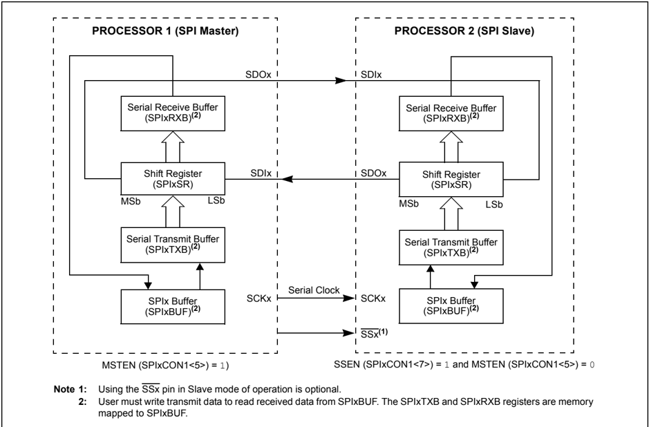
MSTEN (SPIxCON1<5>) = 1 SSEN (SPIxCON1<7>) = 1 and MSTEN (SPIxCON1<5>) = 0
Note 1: Using the \overlineSSx pin in Slave mode of operation is optional. 2: User must write transmit data to read received data from SPIxBUF. The SPIxTXB and SPIxRXB registers are memory mapped to SPIxBUF.
FIGURE 15-4: SPIx MASTER/SLAVE CONNECTION (ENHANCED BUFFER MODES)
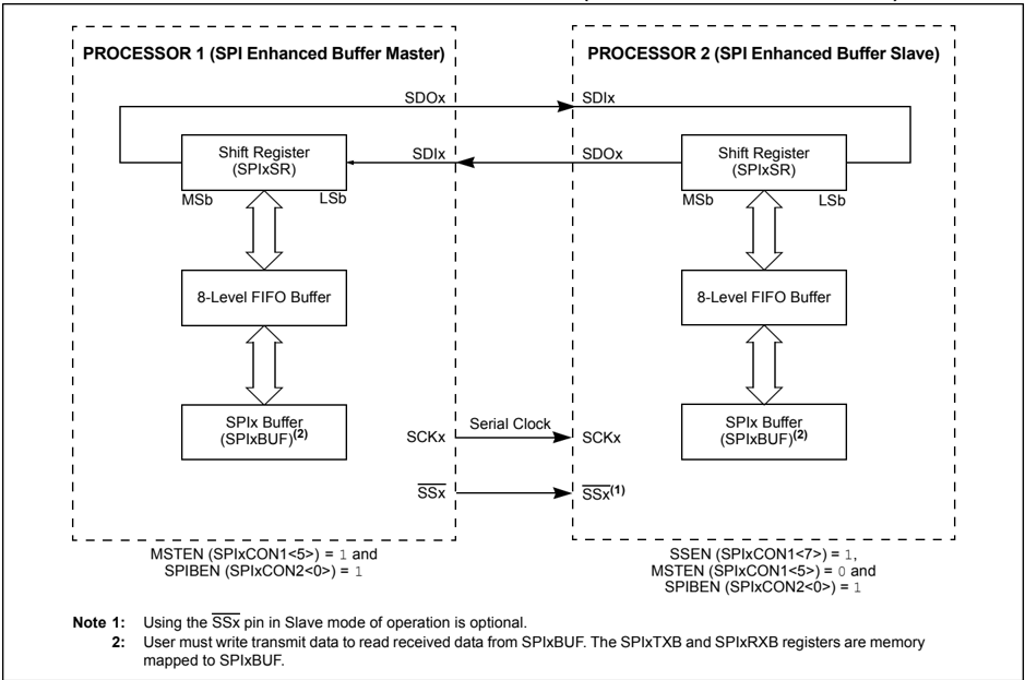
MSTEN (SPIxCON1<5>) = 1 and SPIBEN (SPIxCON2<0>) = 1 SSEN (SPIxCON1<7>) = 1, MSTEN (SPIxCON1<5>) = 0 and SPIBEN (SPIxCON2<0>) = 1
Note 1: Using the \overlineSSx pin in Slave mode of operation is optional. 2: User must write transmit data to read received data from SPIxBUF. The SPIxTXB and SPIxRXB registers are memory mapped to SPIxBUF.
FIGURE 15-5: SPIx MASTER, FRAME MASTER CONNECTION DIAGRAM
 FIGURE 15-6: SPIx MASTER, FRAME SLAVE CONNECTION DIAGRAM
FIGURE 15-7: SPIx SLAVE, FRAME MASTER CONNECTION DIAGRAM
FIGURE 15-8: SPIx SLAVE, FRAME SLAVE CONNECTION DIAGRAM
EQUATION 15-1: RELATIONSHIP BETWEEN DEVICE AND SPIx CLOCK SPEED(1)
FSCK = FCY / (Primary Prescaler * Secondary Prescaler)
Note 1: Based on FCY = FOSC/2; Doze mode and PLL are disabled.
TABLE 15-1: SAMPLE SCKx FREQUENCIES(1,2)
| FCY = 16 MHz | Secondary Prescaler Settings | |||||
|---|---|---|---|---|---|---|
| 1:1 | 2:1 | 4:1 | 6:1 | 8:1 | ||
| Primary Prescaler Settings | 1:1 | Invalid | 8000 | 4000 | 2667 | 2000 |
| 4:1 | 4000 | 2000 | 1000 | 667 | 500 | |
| 16:1 | 1000 | 500 | 250 | 167 | 125 | |
| 64:1 | 250 | 125 | 63 | 42 | 31 |
| FCY = 5 MHz | ||||||
|---|---|---|---|---|---|---|
| Primary Prescaler Settings | 1:1 | 5000 | 2500 | 1250 | 833 | 625 |
| 4:1 | 1250 | 625 | 313 | 208 | 156 | |
| 16:1 | 313 | 156 | 78 | 52 | 39 | |
| 64:1 | 78 | 39 | 20 | 13 | 10 |
Note 1: Based on FCY = FOSC/2; Doze mode and PLL are disabled.
Note 2: SCKx frequencies are shown in kHz.