8.0 OSCILLATOR CONFIGURATION
Note: This data sheet summarizes the features of this group of PIC24F devices. It is not intended to be a comprehensive reference source. For more information, refer to the “PIC24F Family Reference Manual”, “Oscillator” (DS39700).
The oscillator system for PIC24FJ64GA004 family devices has the following features:
- A total of four external and internal oscillator options as clock sources, providing 11 different clock modes
- On-chip 4x PLL to boost internal operating frequency on select internal and external oscillator sources
- Software-controllable switching between various clock sources
- Software-controllable postscaler for selective clocking of CPU for system power savings
- A Fail-Safe Clock Monitor (FSCM) that detects clock failure and permits safe application recovery or shutdown
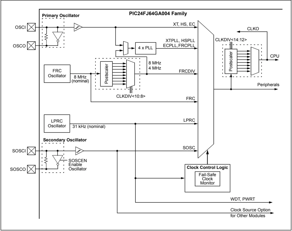
A simplified diagram of the oscillator system is shown in Figure 8-1.
FIGURE 8-1: PIC24FJ64GA004 FAMILY CLOCK DIAGRAM
8.1 CPU Clocking Scheme
The system clock source can be provided by one of four sources:
- Primary Oscillator (POSC) on the OSCI and OSCO pins
- Secondary Oscillator (SOSC) on the SOSC1 and SOSC0 pins
- Fast Internal RC (FRC) Oscillator
- Low-Power Internal RC (LPRC) Oscillator
The primary oscillator and FRC sources have the option of using the internal 4x PLL. The frequency of the FRC clock source can optionally be reduced by the programmable clock divider. The selected clock source generates the processor and peripheral clock sources.
The processor clock source is divided by two to produce the internal instruction cycle clock, FCY. In this document, the instruction cycle clock is also denoted by Fosc/2. The internal instruction cycle clock, Fosc/2, can be provided on the OSCO I/O pin for some operating modes of the primary oscillator.
8.2 Initial Configuration on POR
The oscillator source (and operating mode) that is used at a device Power-on Reset event is selected using Configuration bit settings. The Oscillator Configuration bit settings are located in the Configuration registers in the program memory (refer to Section 24.1 “Configuration Bits” for further details). The Primary Oscillator Configuration bits, POSCMD<1:0> (Configuration Word 2<1:0>), and the Initial Oscillator Select Configuration bits, FNOSC<2:0> (Configuration Word 2<10:8>), select the oscillator source that is used at a Power-on Reset. The FRC Primary Oscillator with Postscaler (FRCDIV) is the default (unprogrammed) selection. The Secondary Oscillator, or one of the internal oscillators, may be chosen by programming these bit locations.
The Configuration bits allow users to choose between the various clock modes, shown in Table 8-1.
8.2.1 CLOCK SWITCHING MODE CONFIGURATION BITS
The FCKSM<1:0> Configuration bits (Configuration Word 2<7:6>) are used to jointly configure device clock switching and the Fail-Safe Clock Monitor (FSCM). Clock switching is enabled only when FCKSM1 is programmed (‘0’). The FSCM is enabled only when FCKSM<1:0> are both programmed (‘00’).
TABLE 8-1: CONFIGURATION BIT VALUES FOR CLOCK SELECTION
| Oscillator Mode | Oscillator Source | POSCMD<1:0> | FNOSC<2:0> | Notes |
|---|---|---|---|---|
| Fast RC Oscillator with Postscaler (FRCDIV) | Internal | 11 | 111 | 1, 2 |
| (Reserved) | Internal | xx | 110 | 1 |
| Low-Power RC Oscillator (LPRC) | Internal | 11 | 101 | 1 |
| Secondary (Timer1) Oscillator (SOSC) | Secondary | 00 | 100 | 1 |
| Primary Oscillator (XT) with PLL Module (XTPLL) | Primary | 01 | 011 | |
| Primary Oscillator (EC) with PLL Module (ECPLL) | Primary | 00 | 011 | |
| Primary Oscillator (HS) | Primary | 10 | 010 | |
| Primary Oscillator (XT) | Primary | 01 | 010 | |
| Primary Oscillator (EC) | Primary | 00 | 010 | |
| Fast RC Oscillator with PLL Module (FRCPLL) | Internal | 11 | 001 | 1 |
| Fast RC Oscillator (FRC) | Internal | 11 | 000 | 1 |
Note 1: OSCO pin function is determined by the OSCIOFCN Configuration bit.
2: This is the default oscillator mode for an unprogrammed (erased) device.
8.3 Control Registers
The operation of the oscillator is controlled by three Special Function Registers:
- OSCCON
- CLKDIV
- OSCTUN
The OSCCON register (Register 8-1) is the main control register for the oscillator. It controls clock source switching and allows the monitoring of clock sources.
The Clock Divider register (Register 8-2) controls the features associated with Doze mode, as well as the postscaler for the FRC oscillator.
The FRC Oscillator Tune register (Register 8-3) allows the user to fine-tune the FRC oscillator over a range of approximately ±12%.
REGISTER 8-1: OSCCON: OSCILLATOR CONTROL REGISTER
| U-0 | R-0 | R-0 | R-0 | U-0 | R/W-x⁽¹⁾ | R/W-x⁽¹⁾ | R/W-x⁽¹⁾ |
|---|---|---|---|---|---|---|---|
| — | COSC2 | COSC1 | COSC0 | — | NOSC2 | NOSC1 | NOSC0 |
| bit 15 | bit 8 |
| R/SO-0 | R/W-0 | R-0⁽³⁾ | U-0 | R/CO-0 | U-0 | R/W-0 | R/W-0 |
|---|---|---|---|---|---|---|---|
| CLKLOCK | IOLOCK⁽²⁾ | LOCK | — | CF | — | SOSCEN | OSWEN |
| bit 7 | bit 0 |
Legend:
| R = Readable bit | CO = Clearable Only bit | SO = Settable Only bit |
|---|---|---|
| -n = Value at POR | W = Writable bit | U = Unimplemented bit, read as ‘0’ |
| ‘1’ = Bit is set | ‘0’ = Bit is cleared | x = Bit is unknown |
bit 15 Unimplemented: Read as ‘0’
bit 14-12 COSC<2:0>: Current Oscillator Selection bits
- 111 = Fast RC Oscillator with Postscaler (FRCDIV)
- 110 = Reserved
- 101 = Low-Power RC Oscillator (LPRC)
- 100 = Secondary Oscillator (SOSC)
- 011 = Primary Oscillator with PLL module (XTPLL, HSPLL, ECPLL)
- 010 = Primary Oscillator (XT, HS, EC)
- 001 = Fast RC Oscillator with Postscaler and PLL module (FRCPLL)
- 000 = Fast RC Oscillator (FRC)
bit 11 Unimplemented: Read as ‘0’
bit 10-8 NOSC<2:0>: New Oscillator Selection bits⁽¹⁾
- 111 = Fast RC Oscillator with Postscaler (FRCDIV)
- 110 = Reserved
- 101 = Low-Power RC Oscillator (LPRC)
- 100 = Secondary Oscillator (SOSC)
- 011 = Primary Oscillator with PLL module (XTPLL, HSPLL, ECPLL)
- 010 = Primary Oscillator (XT, HS, EC)
- 001 = Fast RC Oscillator with Postscaler and PLL module (FRCPLL)
- 000 = Fast RC Oscillator (FRC)
Note 1: Reset values for these bits are determined by the FNOSCx Configuration bits.
2: The state of the IOLOCK bit can only be changed once an unlocking sequence has been executed. In addition, if the IOL1WAY Configuration bit is ‘1’ once the IOLOCK bit is set, it cannot be cleared.
3: Also resets to ‘0’ during any valid clock switch or whenever a non-PLL Clock mode is selected.
REGISTER 8-1: OSCCON: OSCILLATOR CONTROL REGISTER (CONTINUED)
bit 7 CLKLOCK: Clock Selection Lock Enable bit If FSCM is enabled (FCKSM1 = 1): 1 = Clock and PLL selections are locked 0 = Clock and PLL selections are not locked and may be modified by setting the OSWEN bit If FSCM is disabled (FCKSM1 = 0): Clock and PLL selections are never locked and may be modified by setting the OSWEN bit.
bit 6 IOLOCK: I/O Lock Enable bit(2) 1 = I/O lock is active 0 = I/O lock is not active
bit 5 LOCK: PLL Lock Status bit(3) 1 = PLL module is in lock or PLL module start-up timer is satisfied 0 = PLL module is out of lock, PLL start-up timer is running or PLL is disabled
bit 4 Unimplemented: Read as '0'
bit 3 CF: Clock Fail Detect bit 1 = FSCM has detected a clock failure 0 = No clock failure has been detected
bit 2 Unimplemented: Read as '0'
bit 1 SOSCEN: 32 kHz Secondary Oscillator (SOSC) Enable bit 1 = Enables Secondary Oscillator 0 = Disables Secondary Oscillator
bit 0 OSWEN: Oscillator Switch Enable bit 1 = Initiates an oscillator switch to a clock source specified by the NOSC<2:0> bits 0 = Oscillator switch is complete
Note 1: Reset values for these bits are determined by the FNOSCx Configuration bits. 2: The state of the IOLOCK bit can only be changed once an unlocking sequence has been executed. In addition, if the IOL1WAY Configuration bit is '1' once the IOLOCK bit is set, it cannot be cleared. 3: Also resets to '0' during any valid clock switch or whenever a non-PLL Clock mode is selected.
DS39881E-page 98 © 2010-2013 Microchip Technology Inc.
REGISTER 8-2: CLKDIV: CLOCK DIVIDER REGISTER
| R/W-0 | R/W-0 | R/W-1 | R/W-1 | R/W-0 | R/W-0 | R/W-0 | R/W-1 |
|---|---|---|---|---|---|---|---|
| ROI | DOZE2 | DOZE1 | DOZE0 | DOZEN(1) | RCDIV2 | RCDIV1 | RCDIV0 |
| bit 15 | bit 8 |
| U-0 | U-1 | U-0 | U-0 | U-0 | U-0 | U-0 | U-0 |
|---|---|---|---|---|---|---|---|
| — | — | — | — | — | — | — | — |
| bit 7 | bit 0 |
Legend:
R = Readable bit
W = Writable bit
U = Unimplemented bit, read as ‘0’
-n = Value at POR
‘1’ = Bit is set
‘0’ = Bit is cleared
x = Bit is unknown
bit 15
ROI: Recover on Interrupt bit
1 = Interrupts clear the DOZEN bit and reset the CPU peripheral clock ratio to 1:1
0 = Interrupts have no effect on the DOZEN bit
bit 14-12
DOZE<2:0>: CPU Peripheral Clock Ratio Select bits
111 = 1:128
110 = 1:64
101 = 1:32
100 = 1:16
011 = 1:8
010 = 1:4
001 = 1:2
000 = 1:1
bit 11
DOZEN: DOZE Enable bit(1)
1 = DOZE<2:0> bits specify the CPU peripheral clock ratio
0 = CPU peripheral clock ratio is set to 1:1
bit 10-8
RCDIV<2:0>: FRC Postscaler Select bits
111 = 31.25 kHz (divide-by-256)
110 = 125 kHz (divide-by-64)
101 = 250 kHz (divide-by-32)
100 = 500 kHz (divide-by-16)
011 = 1 MHz (divide-by-8)
010 = 2 MHz (divide-by-4)
001 = 4 MHz (divide-by-2)
000 = 8 MHz (divide-by-1)
bit 7
Unimplemented: Read as ‘0’
bit 6
Unimplemented: Read as ‘1’
bit 5-0
Unimplemented: Read as ‘0’
Note 1: This bit is automatically cleared when the ROI bit is set and an interrupt occurs.
REGISTER 8-3: OSCTUN: FRC OSCILLATOR TUNE REGISTER
| U-0 | U-0 | U-0 | U-0 | U-0 | U-0 | U-0 | U-0 |
|---|---|---|---|---|---|---|---|
| — | — | — | — | — | — | — | — |
| bit 15 | bit 8 |
| U-0 | U-0 | R/W-0 | R/W-0 | R/W-0 | R/W-0 | R/W-0 | R/W-0 |
|---|---|---|---|---|---|---|---|
| — | — | TUN5⁽¹⁾ | TUN4⁽¹⁾ | TUN3⁽¹⁾ | TUN2⁽¹⁾ | TUN1⁽¹⁾ | TUN0⁽¹⁾ |
| bit 7 | bit 0 |
Legend:
R = Readable bit
W = Writable bit
U = Unimplemented bit, read as ‘0’
-n = Value at POR
‘1’ = Bit is set
‘0’ = Bit is cleared
x = Bit is unknown
bit 15-6 Unimplemented: Read as ‘0’
bit 5-0 TUN<5:0>: FRC Oscillator Tuning bits⁽¹⁾
011111 = Maximum frequency deviation
011110 =
•
•
•
000001 =
000000 = Center frequency, oscillator is running at factory calibrated frequency
111111 =
•
•
•
100001 =
100000 = Minimum frequency deviation
Note 1: Increments or decrements of TUN<5:0> may not change the FRC frequency in equal steps over the FRC tuning range and may not be monotonic.
8.4 Clock Switching Operation
With few limitations, applications are free to switch between any of the four clock sources (POSC, SOSC, FRC and LPRC) under software control and at any time. To limit the possible side effects that could result from this flexibility, PIC24F devices have a safeguard lock built into the switching process.
Note: The Primary Oscillator mode has three different submodes (XT, HS and EC) which are determined by the POSCMDx Configuration bits. While an application can switch to and from Primary Oscillator mode in software, it cannot switch between the different primary submodes without reprogramming the device.
8.4.1 ENABLING CLOCK SWITCHING
To enable clock switching, the FCKSM1 Configuration bit in Flash Configuration Word 2 must be programmed to ‘0’. (Refer to Section 24.1 “Configuration Bits” for further details.) If the FCKSM1 Configuration bit is unprogrammed (‘1’), the clock switching function and Fail-Safe Clock Monitor function are disabled. This is the default setting.
The NOSCx control bits (OSCCON<10:8>) do not control the clock selection when clock switching is disabled. However, the COSCx bits (OSCCON<14:12>) will reflect the clock source selected by the FNOSCx Configuration bits.
The OSWEN control bit (OSCCON<0>) has no effect when clock switching is disabled; it is held at ‘0’ at all times.
8.4.2 OSCILLATOR SWITCHING SEQUENCE
At a minimum, performing a clock switch requires this basic sequence:
- If desired, read the COSCx bits (OSCCON<14:12>) to determine the current oscillator source.
- Perform the unlock sequence to allow a write to the OSCCON register high byte.
- Write the appropriate value to the NOSCx bits (OSCCON<10:8>) for the new oscillator source.
- Perform the unlock sequence to allow a write to the OSCCON register low byte.
- Set the OSWEN bit to initiate the oscillator switch.
Once the basic sequence is completed, the system clock hardware responds automatically as follows:
- The clock switching hardware compares the COSCx bits with the new value of the NOSCx bits. If they are the same, then the clock switch is a redundant operation. In this case, the OSWEN bit is cleared automatically and the clock switch is aborted.
- If a valid clock switch has been initiated, the LOCK (OSCCON<5>) and CF (OSCCON<3>) bits are cleared.
- The new oscillator is turned on by the hardware if it is not currently running. If a crystal oscillator must be turned on, the hardware will wait until the OST expires. If the new source is using the PLL, then the hardware waits until a PLL lock is detected (LOCK = 1).
- The hardware waits for 10 clock cycles from the new clock source and then performs the clock switch.
- The hardware clears the OSWEN bit to indicate a successful clock transition. In addition, the NOSCx bit values are transferred to the COSCx bits.
- The old clock source is turned off at this time, with the exception of LPRC (if WDT or FSCM are enabled) or SOSC (if SOSCEN remains set).
Note 1: The processor will continue to execute code throughout the clock switching sequence. Timing-sensitive code should not be executed during this time.
2: Direct clock switches between any Primary Oscillator mode with PLL and FRCPLL mode are not permitted. This applies to clock switches in either direction. In these instances, the application must switch to FRC mode as a transitional clock source between the two PLL modes.
A recommended code sequence for a clock switch includes the following:
- Disable interrupts during the OSCCON register unlock and write sequence.
- Execute the unlock sequence for the OSCCON high byte by writing 78h and 9Ah to OSCCON<15:8> in two back-to-back instructions.
- Write the new oscillator source to the NOSCx bits in the instruction immediately following the unlock sequence.
- Execute the unlock sequence for the OSCCON low byte by writing 46h and 57h to OSCCON<7:0> in two back-to-back instructions.
- Set the OSWEN bit in the instruction immediately following the unlock sequence.
- Continue to execute code that is not clock-sensitive (optional).
- Invoke an appropriate amount of software delay (cycle counting) to allow the selected oscillator and/or PLL to start and stabilize.
- Check to see if OSWEN is '0'. If it is, the switch was successful. If OSWEN is still set, then check the LOCK bit to determine the cause of failure.
The core sequence for unlocking the OSCCON register and initiating a clock switch is shown in Example 8-1.
EXAMPLE 8-1: BASIC CODE SEQUENCE FOR CLOCK SWITCHING
.global __reset .include "p24fxxxx.inc" .text __reset: ;Place the new oscillator selection in W0 ;OSCCONH (high byte) Unlock Sequence DISI #18 PUSH w1 PUSH w2 PUSH w3 MOV #OSCCONH, w1 MOV #0x78, w2 MOV #0x9A, w3 MOV.b w2, [w1] MOV.b w3, [w1] ;Set new oscillator selection MOV.b WREG, OSCCONH ;OSCCONL (low byte) unlock sequence MOV #OSCCONL, w1 MOV #0x46, w2 MOV #0x57, w3 MOV.b w2, [w1] MOV.b w3, [w1] ;Start oscillator switch operation BSET OSCCON, #0 POP w3 POP w2 POP w1 .end
8.4.3 SECONDARY OSCILLATOR LOW-POWER OPERATION
Note: This feature is implemented only on PIC24FJ64GA004 family devices with a major silicon revision level of B or later (DEVREV register value is 3042h or greater).
The Secondary Oscillator (SOSC) can operate in two distinct levels of power consumption based on device configuration. In Low-Power mode, the oscillator operates in a low gain, low-power state. By default, the oscillator uses a higher gain setting, and therefore, requires more power. The Secondary Oscillator Mode Selection bits, SOSCSEL<1:0> (CW2<12:11>), determine the oscillator’s power mode.
When Low-Power mode is used, care must be taken in the design and layout of the SOSC circuit to ensure that the oscillator will start up and oscillate properly. The lower gain of this mode makes the SOSC more sensitive to noise and requires a longer start-up time.
8.4.4 OSCILLATOR LAYOUT
On low pin count devices, such as those in the PIC24FJ64GA004 family, due to pinout limitations, the SOSC is more susceptible to noise than other PIC24F devices. Unless proper care is taken in the design and layout of the SOSC circuit, it is possible for inaccuracies to be introduced into the oscillator’s period.
In general, the crystal circuit connections should be as short as possible. It is also good practice to surround the crystal circuit with a ground loop or ground plane. For more detailed information on crystal circuit design, please refer to the “PIC24F Family Reference Manual”, “Oscillator” (DS39700) and Microchip Application Notes: AN826, “Crystal Oscillator Basics and Crystal Selection for rfPIC® and PICmicro® Devices” (DS00826) and AN849, “Basic PICmicro® Oscillator Design” (DS00849).
9.0 POWER-SAVING FEATURES
Note: This data sheet summarizes the features of this group of PIC24F devices. It is not intended to be a comprehensive reference source. For more information, refer to the “PIC24F Family Reference Manual”, “Power-Saving Features” (DS39698). Additional power-saving tips can also be found in Appendix B: “Additional Guidance for PIC24FJ64GA004 Family Applications” of this document.
The PIC24FJ64GA004 family of devices provides the ability to manage power consumption by selectively managing clocking to the CPU and the peripherals. In general, a lower clock frequency and a reduction in the number of circuits being clocked constitutes lower consumed power. All PIC24F devices manage power consumption in four different ways:
- Clock Frequency
- Instruction-Based Sleep and Idle modes
- Software Controlled Doze mode
- Selective Peripheral Control in Software
Combinations of these methods can be used to selectively tailor an application’s power consumption, while still maintaining critical application features, such as timing-sensitive communications.
9.1 Clock Frequency and Clock Switching
PIC24F devices allow for a wide range of clock frequencies to be selected under application control. If the system clock configuration is not locked, users can choose low-power or high-precision oscillators by simply changing the NOSCx bits. The process of changing a system clock during operation, as well as limitations to the process, are discussed in more detail in Section 8.0 “Oscillator Configuration”.
9.2 Instruction-Based Power-Saving Modes
PIC24F devices have two special power-saving modes that are entered through the execution of a special PWRSAV instruction. Sleep mode stops clock operation and halts all code execution; Idle mode halts the CPU and code execution, but allows peripheral modules to continue operation. The assembly syntax of the PWRSAV instruction is shown in Example 9-1.
Sleep and Idle modes can be exited as a result of an enabled interrupt, WDT time-out or a device Reset. When the device exits these modes, it is said to “wake-up”.
Note: SLEEP_MODE and IDLE_MODE are constants defined in the assembler include file for the selected device.
9.2.1 SLEEP MODE
Sleep mode includes these features:
- The system clock source is shut down. If an on-chip oscillator is used, it is turned off.
- The device current consumption will be reduced to a minimum provided that no I/O pin is sourcing current.
- The Fail-Safe Clock Monitor does not operate during Sleep mode since the system clock source is disabled.
- The LPRC clock will continue to run in Sleep mode if the WDT is enabled.
- The WDT, if enabled, is automatically cleared prior to entering Sleep mode.
- Some device features or peripherals may continue to operate in Sleep mode. This includes items such as the Input Change Notification on the I/O ports, or peripherals that use an external clock input. Any peripheral that requires the system clock source for its operation will be disabled in Sleep mode.
Additional power reductions can be achieved by disabling the on-chip voltage regulator whenever Sleep mode is invoked. This is done by clearing the PMSLP bit (RCON<8>). Disabling the regulator adds an additional delay of about 190 µs to the device wake-up time. It is recommended that applications not using the voltage regulator leave the PMSLP bit set. For additional details on the regulator and Sleep mode, see Section 24.2.5 “Voltage Regulator Standby Mode”.
The device will wake-up from Sleep mode on any of these events:
- On any interrupt source that is individually enabled.
- On any form of device Reset.
- On a WDT time-out.
On wake-up from Sleep, the processor will restart with the same clock source that was active when Sleep mode was entered.
EXAMPLE 9-1: PWRSAV INSTRUCTION SYNTAX
9.2.2 IDLE MODE
Idle mode includes these features:
- The CPU will stop executing instructions.
- The WDT is automatically cleared.
- The system clock source remains active. By default, all peripheral modules continue to operate normally from the system clock source, but can also be selectively disabled (see Section 9.4 “Selective Peripheral Module Control”).
- If the WDT or FSCM is enabled, the LPRC will also remain active.
The device will wake from Idle mode on any of these events:
- Any interrupt that is individually enabled.
- Any device Reset.
- A WDT time-out.
On wake-up from Idle, the clock is reapplied to the CPU and instruction execution begins immediately, starting with the instruction following the PWRSAV instruction or the first instruction in the ISR.
9.2.3 INTERRUPTS COINCIDENT WITH POWER SAVE INSTRUCTIONS
Any interrupt that coincides with the execution of a PWRSAV instruction will be held off until entry into Sleep or Idle mode has completed. The device will then wake-up from Sleep or Idle mode.
9.3 Doze Mode
Generally, changing clock speed and invoking one of the power-saving modes are the preferred strategies for reducing power consumption. There may be circumstances, however, where this is not practical. For example, it may be necessary for an application to maintain uninterrupted synchronous communication, even while it is doing nothing else. Reducing system clock speed may introduce communication errors, while using a power-saving mode may stop communications completely.
Doze mode is a simple and effective alternative method to reduce power consumption while the device is still executing code. In this mode, the system clock continues to operate from the same source and at the same speed. Peripheral modules continue to be clocked at the same speed while the CPU clock speed is reduced. Synchronization between the two clock domains is maintained, allowing the peripherals to access the SFRs while the CPU executes code at a slower rate.
Doze mode is enabled by setting the DOZEN bit (CLKDIV<11>). The ratio between peripheral and core clock speed is determined by the DOZE<2:0> bits (CLKDIV<14:12>). There are eight possible configurations, from 1:1 to 1:256, with 1:1 being the default.
It is also possible to use Doze mode to selectively reduce power consumption in event driven applications. This allows clock-sensitive functions, such as synchronous communications, to continue without interruption while the CPU Idles, waiting for something to invoke an interrupt routine. Enabling the automatic return to full-speed CPU operation on interrupts is enabled by setting the ROI bit (CLKDIV<15>). By default, interrupt events have no effect on Doze mode operation.
9.4 Selective Peripheral Module Control
Idle and Doze modes allow users to substantially reduce power consumption by slowing or stopping the CPU clock. Even so, peripheral modules still remain clocked and thus, consume power. There may be cases where the application needs what these modes do not provide: the allocation of power resources to CPU processing with minimal power consumption from the peripherals.
PIC24F devices address this requirement by allowing peripheral modules to be selectively disabled, reducing or eliminating their power consumption. This can be done with two control bits:
- The Peripheral Enable bit, generically named, “XXXEN”, located in the module’s main control SFR.
- The Peripheral Module Disable (PMD) bit, generically named, “XXXMD”, located in one of the PMD control registers.
Both bits have similar functions in enabling or disabling its associated module. Setting the PMD bit for a module disables all clock sources to that module, reducing its power consumption to an absolute minimum. In this state, the control and status registers associated with the peripheral will also be disabled, so writes to those registers will have no effect and read values will be invalid. Many peripheral modules have a corresponding PMD bit.
In contrast, disabling a module by clearing its XXXEN bit disables its functionality, but leaves its registers available to be read and written to. Power consumption is reduced, but not by as much as the PMD bit does. Most peripheral modules have an enable bit; exceptions include capture, compare and RTCC.
To achieve more selective power savings, peripheral modules can also be selectively disabled when the device enters Idle mode. This is done through the control bit of the generic name format, “XXXIDL”. By default, all modules that can operate during Idle mode will do so. Using the disable on Idle feature allows further reduction of power consumption during Idle mode, enhancing power savings for extremely critical power applications.
DS39881E-page 104 © 2010-2013 Microchip Technology Inc.
10.0 I/O PORTS
Note: This data sheet summarizes the features of this group of PIC24F devices. It is not intended to be a comprehensive reference source. For more information, refer to the "PIC24F Family Reference Manual", "I/O Ports with Peripheral Pin Select (PPS)" (DS39711).
All of the device pins (except VDD, VSS, \overlineMCLR and OSCI/CLKI) are shared between the peripherals and the Parallel I/O (PIO) ports. All I/O input ports feature Schmitt Trigger inputs for improved noise immunity.
10.1 Parallel I/O (PIO) Ports
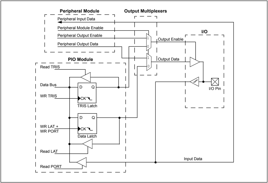
A Parallel I/O port that shares a pin with a peripheral is, in general, subservient to the peripheral. The peripheral's output buffer data and control signals are provided to a pair of multiplexers. The multiplexers select whether the peripheral or the associated port has ownership of the output data and control signals of the I/O pin. The logic also prevents "loop through", in which a port's digital output can drive the input of a peripheral that shares the same pin. Figure 10-1 shows how ports are shared with other peripherals and the associated I/O pin to which they are connected.
When a peripheral is enabled and the peripheral is actively driving an associated pin, the use of the pin as a general purpose output pin is disabled. The I/O pin may be read, but the output driver for the parallel port bit will be disabled. If a peripheral is enabled, but the peripheral is not actively driving a pin, that pin may be driven by a port.
All port pins have three registers directly associated with their operation as digital I/O. The Data Direction register (TRISx) determines whether the pin is an input or an output. If the data direction bit is a '1', then the pin is an input. All port pins are defined as inputs after a Reset. Reads from the Output Latch register (LATx), read the latch. Writes to the latch, write the latch. Reads from the port (PORTx), read the port pins, while writes to the port pins, write the latch.
Any bit and its associated data and control registers that are not valid for a particular device will be disabled. That means the corresponding LATx and TRISx registers and the port pin will read as zeros.
When a pin is shared with another peripheral or function that is defined as an input only, it is nevertheless, regarded as a dedicated port because there is no other competing source of outputs.
FIGURE 10-1: BLOCK DIAGRAM OF A TYPICAL SHARED PORT STRUCTURE
10.1.1 OPEN-DRAIN CONFIGURATION
In addition to the PORT, LAT and TRIS registers for data control, each port pin can also be individually configured for either digital or open-drain output. This is controlled by the Open-Drain Control register, ODCx, associated with each port. Setting any of the bits configures the corresponding pin to act as an open-drain output.
The open-drain feature allows the generation of outputs higher than VDD (e.g., 5V) on any desired digital only pins by using external pull-up resistors. The maximum open-drain voltage allowed is the same as the maximum VIH specification.
10.2 Configuring Analog Port Pins
The use of the AD1PCFG and TRIS registers control the operation of the A/D port pins. The port pins that are desired as analog inputs must have their corresponding TRIS bit set (input). If the TRIS bit is cleared (output), the digital output level (VOH or VOL) will be converted.
When reading the PORT register, all pins configured as analog input channels will read as cleared (a low level). Pins configured as digital inputs will not convert an analog input. Analog levels on any pin that is defined as a digital input (including the ANx pins) may cause the input buffer to consume current that exceeds the device specifications.
10.2.1 I/O PORT WRITE/READ TIMING
One instruction cycle is required between a port direction change or port write operation and a read operation of the same port. Typically, this instruction would be a NOP.
10.2.2 ANALOG INPUT PINS AND VOLTAGE CONSIDERATIONS
The voltage tolerance of pins used as device inputs is dependent on the pin’s input function. Pins that are used as digital only inputs are able to handle DC voltages up to 5.5V, a level typical for digital logic circuits. In contrast, pins that also have analog input functions of any kind can only tolerate voltages up to VDD. Voltage excursions beyond VDD on these pins are always to be avoided. Table 10-1 summarizes the input capabilities. Refer to Section 27.1 “DC Characteristics” for more details.
TABLE 10-1: INPUT VOLTAGE LEVELS
| Port or Pin | Tolerated Input | Description |
|---|---|---|
| PORTA<4:0> | VDD | Only VDD input levels are tolerated. |
| PORTB<15:12> | ||
| PORTB<4:0> | ||
| PORTC<2:0>(1) | ||
| PORTA<10:7>(1) | 5.5V | Tolerates input levels above VDD, useful for |
| PORTB<11:5> | most standard logic. | |
| PORTC<9:3>(1) |
Note 1: Unavailable on 28-pin devices.
10.3 Input Change Notification
The Input Change Notification function of the I/O ports allows the PIC24FJ64GA004 family of devices to generate interrupt requests to the processor in response to a Change-of-State (COS) on selected input pins. This feature is capable of detecting input Change-of-States even in Sleep mode, when the clocks are disabled. Depending on the device pin count, there are up to 22 external signals that may be selected (enabled) for generating an interrupt request on a Change-of-State.
There are four control registers associated with the CN module. The CNEN1 and CNEN2 registers contain the interrupt enable control bits for each of the CN input pins. Setting any of these bits enables a CN interrupt for the corresponding pins.
Each CN pin also has a weak pull-up connected to it. The pull-ups act as a current source that is connected to the pin, and eliminate the need for external resistors when push button or keypad devices are connected. The pull-ups are enabled separately using the CNPU1 and CNPU2 registers, which contain the control bits for each of the CN pins. Setting any of the control bits enables the weak pull-ups for the corresponding pins.
When the internal pull-up is selected, the pin pulls up to VDD – 0.7V (typical). Make sure that there is no external pull-up source when the internal pull-ups are enabled, as the voltage difference can cause a current path.
Note: Pull-ups on Change Notification pins should always be disabled whenever the port pin is configured as a digital output.
EXAMPLE 10-1: PORT WRITE/READ EXAMPLE
MOV 0xFF00, W0 ; Configure PORTB<15:8> as inputs MOV W0, TRISBB ; and PORTB<7:0> as outputs NOP ; Delay 1 cycle BTSS PORTB, #13 ; Next Instruction
10.4 Peripheral Pin Select (PPS)
A major challenge in general purpose devices is providing the largest possible set of peripheral features while minimizing the conflict of features on I/O pins. The challenge is even greater on low pin count devices similar to the PIC24FJ64GA family. In an application that needs to use more than one peripheral multiplexed on a single pin, inconvenient work arounds in application code or a complete redesign may be the only option.
The Peripheral Pin Select feature provides an alternative to these choices by enabling the user's peripheral set selection and their placement on a wide range of I/O pins. By increasing the pinout options available on a particular device, users can better tailor the microcontroller to their entire application, rather than trimming the application to fit the device.
The Peripheral Pin Select feature operates over a fixed subset of digital I/O pins. Users may independently map the input and/or output of any one of many digital peripherals to any one of these I/O pins. Peripheral Pin Select is performed in software and generally does not require the device to be reprogrammed. Hardware safeguards are included that prevent accidental or spurious changes to the peripheral mapping once it has been established.
10.4.1 AVAILABLE PINS
The Peripheral Pin Select feature is used with a range of up to 26 pins; the number of available pins is dependent on the particular device and its pin count. Pins that support the Peripheral Pin Select feature include the designation, "RPn", in their full pin designation, where "RP" designates a remappable peripheral and "n" is the remappable pin number. See Table 1-2 for pinout options in each package offering.
10.4.2 AVAILABLE PERIPHERALS
The peripherals managed by the Peripheral Pin Select are all digital only peripherals. These include general serial communications (UART and SPI), general purpose timer clock inputs, timer-related peripherals (input capture and output compare) and external interrupt inputs. Also included are the outputs of the comparator module, since these are discrete digital signals.
The Peripheral Pin Select module is not applied to I²C™, Change Notification inputs, RTCC alarm outputs or peripherals with analog inputs.
A key difference between pin select and non-pin select peripherals is that pin select peripherals are not associated with a default I/O pin. The peripheral must always be assigned to a specific I/O pin before it can be used. In contrast, non-pin select peripherals are always available on a default pin, assuming that the peripheral is active and not conflicting with another peripheral.
10.4.2.1 Peripheral Pin Select Function Priority
Pin-selectable peripheral outputs (for example, OC and UART transmit) take priority over any general purpose digital functions permanently tied to that pin, such as PMP and port I/O. Specialized digital outputs, such as USB functionality, take priority over PPS outputs on the same pin. The pin diagrams at the beginning of this data sheet list peripheral outputs in order of priority. Refer to them for priority concerns on a particular pin.
Unlike devices with fixed peripherals, pin-selectable peripheral inputs never take ownership of a pin. The pin's output buffer is controlled by the pin's TRIS bit setting or by a fixed peripheral on the pin. If the pin is configured in Digital mode, then the PPS input will operate correctly, reading the input. If an analog function is enabled on the same pin, the pin-selectable input will be disabled.
10.4.3 CONTROLLING PERIPHERAL PIN SELECT
Peripheral Pin Select features are controlled through two sets of Special Function Registers: one to map peripheral inputs and one to map outputs. Because they are separately controlled, a particular peripheral's input and output (if the peripheral has both) can be placed on any selectable function pin without constraint.
The association of a peripheral to a peripheral-selectable pin is handled in two different ways, depending on if an input or an output is being mapped.
10.4.3.1 Input Mapping
The inputs of the Peripheral Pin Select options are mapped on the basis of the peripheral; that is, a control register associated with a peripheral dictates the pin it will be mapped to. The RPINRx registers are used to configure peripheral input mapping (see Register 10-1 through Register 10-14). Each register contains two sets of 5-bit fields, with each set associated with one of the pin-selectable peripherals. Programming a given peripheral's bit field with an appropriate 5-bit value maps the RPn pin with that value to that peripheral. For any given device, the valid range of values for any of the bit fields corresponds to the maximum number of Peripheral Pin Selections supported by the device.
TABLE 10-2: SELECTABLE INPUT SOURCES (MAPS INPUT TO FUNCTION)(1)
| Input Name | Function Name | Register | Configuration Bits |
|---|---|---|---|
| External Interrupt 1 | INT1 | RPINR0 | INTR1<4:0> |
| External Interrupt 2 | INT2 | RPINR1 | INTR2R<4:0> |
| Timer2 External Clock | T2CK | RPINR3 | T2CKR<4:0> |
| Timer3 External Clock | T3CK | RPINR3 | T3CKR<4:0> |
| Timer4 External Clock | T4CK | RPINR4 | T4CKR<4:0> |
| Timer5 External Clock | T5CK | RPINR4 | T5CKR<4:0> |
| Input Capture 1 | IC1 | RPINR7 | IC1R<4:0> |
| Input Capture 2 | IC2 | RPINR7 | IC2R<4:0> |
| Input Capture 3 | IC3 | RPINR8 | IC3R<4:0> |
| Input Capture 4 | IC4 | RPINR8 | IC4R<4:0> |
| Input Capture 5 | IC5 | RPINR9 | IC5R<4:0> |
| Output Compare Fault A | OCFA | RPINR11 | OCFAR<4:0> |
| Output Compare Fault B | OCFB | RPINR11 | OCFBR<4:0> |
| UART1 Receive | U1RX | RPINR18 | U1RXR<4:0> |
| UART1 Clear-to-Send | U1CTS | RPINR18 | U1CTSR<4:0> |
| UART2 Receive | U2RX | RPINR19 | U2RXR<4:0> |
| UART2 Clear-to-Send | U2CTS | RPINR19 | U2CTSR<4:0> |
| SPI1 Data Input | SDI1 | RPINR20 | SDI1R<4:0> |
| SPI1 Clock Input | SCK1IN | RPINR20 | SCK1R<4:0> |
| SPI1 Slave Select Input | SS1IN | RPINR21 | SS1R<4:0> |
| SPI2 Data Input | SDI2 | RPINR22 | SDI2R<4:0> |
| SPI2 Clock Input | SCK2IN | RPINR22 | SCK2R<4:0> |
| SPI2 Slave Select Input | SS2IN | RPINR23 | SS2R<4:0> |
Note 1: Unless otherwise noted, all inputs use the Schmitt Trigger input buffers.
10.4.3.2 Output Mapping
In contrast to inputs, the outputs of the Peripheral Pin Select options are mapped on the basis of the pin. In this case, a control register associated with a particular pin dictates the peripheral output to be mapped. The RPORx registers are used to control output mapping. Like the RPINRx registers, each register contains two 5-bit fields; each field being associated with one RPn pin (see Register 10-15 through Register 10-27). The value of the bit field corresponds to one of the peripherals and that peripheral’s output is mapped to the pin (see Table 10-3).
Because of the mapping technique, the list of peripherals for output mapping also includes a null value of ‘00000’. This permits any given pin to remain disconnected from the output of any of the pin-selectable peripherals.
TABLE 10-3: SELECTABLE OUTPUT SOURCES (MAPS FUNCTION TO OUTPUT)
| Function | Output Function Number(1) | Output Name |
|---|---|---|
| NULL(2) | 0 | NULL |
| C1OUT | 1 | Comparator 1 Output |
| C2OUT | 2 | Comparator 2 Output |
| U1TX | 3 | UART1 Transmit |
| U1RTS(3) | 4 | UART1 Request-to-Send |
| U2TX | 5 | UART2 Transmit |
| U2RTS(3) | 6 | UART2 Request-to-Send |
| SDO1 | 7 | SPI1 Data Output |
| SCK1OUT | 8 | SPI1 Clock Output |
| SS1OUT | 9 | SPI1 Slave Select Output |
| SDO2 | 10 | SPI2 Data Output |
| SCK2OUT | 11 | SPI2 Clock Output |
| SS2OUT | 12 | SPI2 Slave Select Output |
| OC1 | 18 | Output Compare 1 |
| OC2 | 19 | Output Compare 2 |
| OC3 | 20 | Output Compare 3 |
| OC4 | 21 | Output Compare 4 |
| OC5 | 22 | Output Compare 5 |
Note 1: Value assigned to the RPn<4:0> pins corresponds to the peripheral output function number.
2: The NULL function is assigned to all RPn outputs at device Reset and disables the RPn output function.
3: IrDA® BCLK functionality uses this output.
10.4.3.3 Mapping Limitations
The control schema of the Peripheral Pin Select is extremely flexible. Other than systematic blocks that prevent signal contention, caused by two physical pins being configured as the same functional input or two functional outputs configured as the same pin, there are no hardware enforced lockouts. The flexibility extends to the point of allowing a single input to drive multiple peripherals or a single functional output to drive multiple output pins.
10.4.4 CONTROLLING CONFIGURATION CHANGES
Because peripheral remapping can be changed during run time, some restrictions on peripheral remapping are needed to prevent accidental configuration changes. PIC24F devices include three features to prevent alterations to the peripheral map:
- Control register lock sequence
- Continuous state monitoring
- Configuration bit remapping lock
10.4.4.1 Control Register Lock
Under normal operation, writes to the RPINRx and RPORx registers are not allowed. Attempted writes will appear to execute normally, but the contents of the registers will remain unchanged. To change these registers, they must be unlocked in hardware. The register lock is controlled by the IOLOCK bit (OSCCON<6>). Setting IOLOCK prevents writes to the control registers; clearing IOLOCK allows writes.
To set or clear IOLOCK, a specific command sequence must be executed:
- Write 46h to OSCCON<7:0>.
- Write 57h to OSCCON<7:0>.
- Clear (or set) IOLOCK as a single operation.
Unlike the similar sequence with the oscillator’s LOCK bit, IOLOCK remains in one state until changed. This allows all of the Peripheral Pin Selects to be configured with a single unlock sequence, followed by an update to all control registers, then locked with a second lock sequence.
10.4.4.2 Continuous State Monitoring
In addition to being protected from direct writes, the contents of the RPINRx and RPORx registers are constantly monitored in hardware by shadow registers. If an unexpected change in any of the registers occurs (such as cell disturbances caused by ESD or other external events), a Configuration Mismatch Reset will be triggered.
10.4.4.3 Configuration Bit Pin Select Lock
As an additional level of safety, the device can be configured to prevent more than one write session to the RPINRx and RPORx registers. The IOL1WAY (CW2<4>) Configuration bit blocks the IOLOCK bit from being cleared after it has been set once. If IOLOCK remains set, the register unlock procedure will not execute and the Peripheral Pin Select Control registers cannot be written to. The only way to clear the bit and re-enable peripheral remapping is to perform a device Reset.
In the default (unprogrammed) state, IOL1WAY is set, restricting users to one write session. Programming IOL1WAY allows users unlimited access (with the proper use of the unlock sequence) to the Peripheral Pin Select registers.
10.4.5 CONSIDERATIONS FOR PERIPHERAL PIN SELECTION
The ability to control Peripheral Pin Selection introduces several considerations into application design that could be overlooked. This is particularly true for several common peripherals that are available only as remappable peripherals.
The main consideration is that the Peripheral Pin Selects are not available on default pins in the device’s default (Reset) state. Since all RPINRx registers reset to ‘11111’ and all RPORx registers reset to ‘00000’, all Peripheral Pin Select inputs are tied to RP31 and all Peripheral Pin Select outputs are disconnected.
Note: In tying Peripheral Pin Select inputs to RP31, RP31 does not have to exist on a device for the registers to be reset to it.
This situation requires the user to initialize the device with the proper peripheral configuration before any other application code is executed. Since the IOLOCK bit resets in the unlocked state, it is not necessary to execute the unlock sequence after the device has come out of Reset. For application safety, however, it is best to set IOLOCK and lock the configuration after writing to the control registers.
Because the unlock sequence is timing critical, it must be executed as an assembly language routine in the same manner as changes to the oscillator configuration. If the bulk of the application is written in C or another high-level language, the unlock sequence should be performed by writing in-line assembly.
Choosing the configuration requires the review of all Peripheral Pin Selects and their pin assignments, especially those that will not be used in the application. In all cases, unused pin-selectable peripherals should be disabled completely. Unused peripherals should have their inputs assigned to an unused RPn pin function. I/O pins with unused RPn functions should be configured with the null peripheral output.
The assignment of a peripheral to a particular pin does not automatically perform any other configuration of the pin’s I/O circuitry. In theory, this means adding a pin-selectable output to a pin may mean inadvertently driving an existing peripheral input when the output is driven. Users must be familiar with the behavior of other fixed peripherals that share a remappable pin and know when to enable or disable them. To be safe, fixed digital peripherals that share the same pin should be disabled when not in use.
Along these lines, configuring a remappable pin for a specific peripheral does not automatically turn that feature on. The peripheral must be specifically configured for operation and enabled, as if it were tied to a fixed pin. Where this happens in the application code (immediately following device Reset and peripheral configuration or inside the main application routine) depends on the peripheral and its use in the application.
A final consideration is that Peripheral Pin Select functions neither override analog inputs, nor reconfigure pins with analog functions for digital I/O. If a pin is configured as an analog input on device Reset, it must be explicitly reconfigured as a digital I/O when used with a Peripheral Pin Select.
Example 10-2 shows a configuration for bidirectional communication with flow control using UART1. The following input and output functions are used:
- Input Functions: U1RX, U1CTS
- Output Functions: U1TX, U1RTS
EXAMPLE 10-2: CONFIGURING UART1 INPUT AND OUTPUT FUNCTIONS
// Unlock Registers __builtin_write_OSCCONL(OSCCON & 0xBF);
// Configure Input Functions (Table 10-2) // Assign U1RX To Pin RP0 RPINR18bits.U1RXR = 0; // Assign U1CTS To Pin RP1 RPINR18bits.U1CTSR = 1; // Configure Output Functions (Table 10-3) // Assign U1TX To Pin RP2 RPOR1bits.RP2R = 3; // Assign U1RTS To Pin RP3 RPOR1bits.RP3R = 4;
// Lock Registers __builtin_write_OSCCONL(OSCCON | 0x40);
10.5 Peripheral Pin Select Registers
The PIC24FJ64GA004 family of devices implements a total of 27 registers for remappable peripheral configuration:
- Input Remappable Peripheral Registers (14)
- Output Remappable Peripheral Registers (13)
Note: Input and output register values can only be changed if IOLock (OSCCON<6>) = 0. See Section 10.4.4.1 “Control Register Lock” for a specific command sequence.
REGISTER 10-1: RPINR0: PERIPHERAL PIN SELECT INPUT REGISTER 0
| U-0 | U-0 | U-0 | R/W-1 | R/W-1 | R/W-1 | R/W-1 | R/W-1 |
|---|---|---|---|---|---|---|---|
| — | — | — | INT1R4 | INT1R3 | INT1R2 | INT1R1 | INT1R0 |
| bit 15 | bit 8 |
| U-0 | U-0 | U-0 | U-0 | U-0 | U-0 | U-0 | U-0 |
|---|---|---|---|---|---|---|---|
| — | — | — | — | — | — | — | — |
| bit 7 | bit 0 |
Legend: R = Readable bit W = Writable bit U = Unimplemented bit, read as ‘0’ -n = Value at POR ‘1’ = Bit is set ‘0’ = Bit is cleared x = Bit is unknown
bit 15-13 Unimplemented: Read as ‘0’ bit 12-8 INT1R<4:0>: Assign External Interrupt 1 (INT1) to the Corresponding RPn Pin bits bit 7-0 Unimplemented: Read as ‘0’
REGISTER 10-2: RPINR1: PERIPHERAL PIN SELECT INPUT REGISTER 1
| U-0 | U-0 | U-0 | U-0 | U-0 | U-0 | U-0 | U-0 |
|---|---|---|---|---|---|---|---|
| — | — | — | — | — | — | — | — |
| bit 15 | bit 8 |
| U-0 | U-0 | U-0 | R/W-1 | R/W-1 | R/W-1 | R/W-1 | R/W-1 |
|---|---|---|---|---|---|---|---|
| — | — | — | INT2R4 | INT2R3 | INT2R2 | INT2R1 | INT2R0 |
| bit 7 | bit 0 |
Legend: R = Readable bit W = Writable bit U = Unimplemented bit, read as ‘0’ -n = Value at POR ‘1’ = Bit is set ‘0’ = Bit is cleared x = Bit is unknown
bit 15-5 Unimplemented: Read as ‘0’ bit 4-0 INT2R<4:0>: Assign External Interrupt 2 (INT2) to the Corresponding RPn Pin bits
REGISTER 10-3: RPINR3: PERIPHERAL PIN SELECT INPUT REGISTER 3
| U-0 | U-0 | U-0 | R/W-1 | R/W-1 | R/W-1 | R/W-1 | R/W-1 |
|---|---|---|---|---|---|---|---|
| — | — | — | T3CKR4 | T3CKR3 | T3CKR2 | T3CKR1 | T3CKR0 |
| bit 15 | bit 8 |
| U-0 | U-0 | U-0 | R/W-1 | R/W-1 | R/W-1 | R/W-1 | R/W-1 |
|---|---|---|---|---|---|---|---|
| — | — | — | T2CKR4 | T2CKR3 | T2CKR2 | T2CKR1 | T2CKR0 |
| bit 7 | bit 0 |
Legend:
R = Readable bit
W = Writable bit
U = Unimplemented bit, read as ‘0’
-n = Value at POR
‘1’ = Bit is set
‘0’ = Bit is cleared
x = Bit is unknown
bit 15-13 Unimplemented: Read as ‘0’
bit 12-8 T3CKR<4:0>: Assign Timer3 External Clock (T3CK) to the Corresponding RPn Pin bits
bit 7-5 Unimplemented: Read as ‘0’
bit 4-0 T2CKR<4:0>: Assign Timer2 External Clock (T2CK) to the Corresponding RPn Pin bits
REGISTER 10-4: RPINR4: PERIPHERAL PIN SELECT INPUT REGISTER 4
| U-0 | U-0 | U-0 | R/W-1 | R/W-1 | R/W-1 | R/W-1 | R/W-1 |
|---|---|---|---|---|---|---|---|
| — | — | — | T5CKR4 | T5CKR3 | T5CKR2 | T5CKR1 | T5CKR0 |
| bit 15 | bit 8 |
| U-0 | U-0 | U-0 | R/W-1 | R/W-1 | R/W-1 | R/W-1 | R/W-1 |
|---|---|---|---|---|---|---|---|
| — | — | — | T4CKR4 | T4CKR3 | T4CKR2 | T4CKR1 | T4CKR0 |
| bit 7 | bit 0 |
Legend:
R = Readable bit
W = Writable bit
U = Unimplemented bit, read as ‘0’
-n = Value at POR
‘1’ = Bit is set
‘0’ = Bit is cleared
x = Bit is unknown
bit 15-13 Unimplemented: Read as ‘0’
bit 12-8 T5CKR<4:0>: Assign Timer5 External Clock (T5CK) to the Corresponding RPn Pin bits
bit 7-5 Unimplemented: Read as ‘0’
bit 4-0 T4CKR<4:0>: Assign Timer4 External Clock (T4CK) to the Corresponding RPn Pin bits
REGISTER 10-5: RPINR7: PERIPHERAL PIN SELECT INPUT REGISTER 7
| U-0 | U-0 | U-0 | R/W-1 | R/W-1 | R/W-1 | R/W-1 | R/W-1 |
|---|---|---|---|---|---|---|---|
| — | — | — | IC2R4 | IC2R3 | IC2R2 | IC2R1 | IC2R0 |
| bit 15 | bit 8 |
| U-0 | U-0 | U-0 | R/W-1 | R/W-1 | R/W-1 | R/W-1 | R/W-1 |
|---|---|---|---|---|---|---|---|
| — | — | — | IC1R4 | IC1R3 | IC1R2 | IC1R1 | IC1R0 |
| bit 7 | bit 0 |
Legend:
R = Readable bit W = Writable bit U = Unimplemented bit, read as ‘0’ -n = Value at POR ‘1’ = Bit is set ‘0’ = Bit is cleared x = Bit is unknown
bit 15-13 Unimplemented: Read as ‘0’ bit 12-8 IC2R<4:0>: Assign Input Capture 2 (IC2) to the Corresponding RPn Pin bits bit 7-5 Unimplemented: Read as ‘0’ bit 4-0 IC1R<4:0>: Assign Input Capture 1 (IC1) to the Corresponding RPn Pin bits
REGISTER 10-6: RPINR8: PERIPHERAL PIN SELECT INPUT REGISTER 8
| U-0 | U-0 | U-0 | R/W-1 | R/W-1 | R/W-1 | R/W-1 | R/W-1 |
|---|---|---|---|---|---|---|---|
| — | — | — | IC4R4 | IC4R3 | IC4R2 | IC4R1 | IC4R0 |
| bit 15 | bit 8 |
| U-0 | U-0 | U-0 | R/W-1 | R/W-1 | R/W-1 | R/W-1 | R/W-1 |
|---|---|---|---|---|---|---|---|
| — | — | — | IC3R4 | IC3R3 | IC3R2 | IC3R1 | IC3R0 |
| bit 7 | bit 0 |
Legend:
R = Readable bit W = Writable bit U = Unimplemented bit, read as ‘0’ -n = Value at POR ‘1’ = Bit is set ‘0’ = Bit is cleared x = Bit is unknown
bit 15-13 Unimplemented: Read as ‘0’ bit 12-8 IC4R<4:0>: Assign Input Capture 4 (IC4) to the Corresponding RPn Pin bits bit 7-5 Unimplemented: Read as ‘0’ bit 4-0 IC3R<4:0>: Assign Input Capture 3 (IC3) to the Corresponding RPn Pin bits
REGISTER 10-7: RPINR9: PERIPHERAL PIN SELECT INPUT REGISTER 9
| U-0 | U-0 | U-0 | U-0 | U-0 | U-0 | U-0 | U-0 |
|---|---|---|---|---|---|---|---|
| — | — | — | — | — | — | — | — |
| bit 15 | bit 8 |
| U-0 | U-0 | U-0 | R/W-1 | R/W-1 | R/W-1 | R/W-1 | R/W-1 |
|---|---|---|---|---|---|---|---|
| — | — | — | IC5R4 | IC5R3 | IC5R2 | IC5R1 | IC5R0 |
| bit 7 | bit 0 |
Legend:
R = Readable bit W = Writable bit U = Unimplemented bit, read as ‘0’ -n = Value at POR ‘1’ = Bit is set ‘0’ = Bit is cleared x = Bit is unknown
bit 15-5 Unimplemented: Read as ‘0’ bit 4-0 IC5R<4:0>: Assign Input Capture 5 (IC5) to the Corresponding RPn Pin bits
REGISTER 10-8: RPINR11: PERIPHERAL PIN SELECT INPUT REGISTER 11
| U-0 | U-0 | U-0 | R/W-1 | R/W-1 | R/W-1 | R/W-1 | R/W-1 |
|---|---|---|---|---|---|---|---|
| — | — | — | OCFBR4 | OCFBR3 | OCFBR2 | OCFBR1 | OCFBR0 |
| bit 15 | bit 8 |
| U-0 | U-0 | U-0 | R/W-1 | R/W-1 | R/W-1 | R/W-1 | R/W-1 |
|---|---|---|---|---|---|---|---|
| — | — | — | OCFAR4 | OCFAR3 | OCFAR2 | OCFAR1 | OCFAR0 |
| bit 7 | bit 0 |
Legend:
R = Readable bit W = Writable bit U = Unimplemented bit, read as ‘0’ -n = Value at POR ‘1’ = Bit is set ‘0’ = Bit is cleared x = Bit is unknown
bit 15-13 Unimplemented: Read as ‘0’ bit 12-8 OCFBR<4:0>: Assign Output Compare Fault B (OCFB) to the Corresponding RPn Pin bits bit 7-5 Unimplemented: Read as ‘0’ bit 4-0 OCFAR<4:0>: Assign Output Compare Fault A (OCFA) to the Corresponding RPn Pin bits
REGISTER 10-9: RPINR18: PERIPHERAL PIN SELECT INPUT REGISTER 18
| U-0 | U-0 | U-0 | R/W-1 | R/W-1 | R/W-1 | R/W-1 | R/W-1 |
|---|---|---|---|---|---|---|---|
| — | — | — | U1CTSR4 | U1CTSR3 | U1CTSR2 | U1CTSR1 | U1CTSR0 |
| bit 15 | bit 8 |
| U-0 | U-0 | U-0 | R/W-1 | R/W-1 | R/W-1 | R/W-1 | R/W-1 |
|---|---|---|---|---|---|---|---|
| — | — | — | U1RXR4 | U1RXR3 | U1RXR2 | U1RXR1 | U1RXR0 |
| bit 7 | bit 0 |
Legend:
R = Readable bit W = Writable bit U = Unimplemented bit, read as ‘0’ -n = Value at POR ‘1’ = Bit is set ‘0’ = Bit is cleared x = Bit is unknown
bit 15-13 Unimplemented: Read as ‘0’ bit 12-8 U1CTSR<4:0>: Assign UART1 Clear-to-Send (U1CTS) to the Corresponding RPn Pin bits bit 7-5 Unimplemented: Read as ‘0’ bit 4-0 U1RXR<4:0>: Assign UART1 Receive (U1RX) to the Corresponding RPn Pin bits
REGISTER 10-10: RPINR19: PERIPHERAL PIN SELECT INPUT REGISTER 19
| U-0 | U-0 | U-0 | R/W-1 | R/W-1 | R/W-1 | R/W-1 | R/W-1 |
|---|---|---|---|---|---|---|---|
| — | — | — | U2CTSR4 | U2CTSR3 | U2CTSR2 | U2CTSR1 | U2CTSR0 |
| bit 15 | bit 8 |
| U-0 | U-0 | U-0 | R/W-1 | R/W-1 | R/W-1 | R/W-1 | R/W-1 |
|---|---|---|---|---|---|---|---|
| — | — | — | U2RXR4 | U2RXR3 | U2RXR2 | U2RXR1 | U2RXR0 |
| bit 7 | bit 0 |
Legend:
R = Readable bit W = Writable bit U = Unimplemented bit, read as ‘0’ -n = Value at POR ‘1’ = Bit is set ‘0’ = Bit is cleared x = Bit is unknown
bit 15-13 Unimplemented: Read as ‘0’ bit 12-8 U2CTSR<4:0>: Assign UART2 Clear-to-Send (U2CTS) to the Corresponding RPn Pin bits bit 7-5 Unimplemented: Read as ‘0’ bit 4-0 U2RXR<4:0>: Assign UART2 Receive (U2RX) to the Corresponding RPn Pin bits
REGISTER 10-11: RPINR20: PERIPHERAL PIN SELECT INPUT REGISTER 20
| U-0 | U-0 | U-0 | R/W-1 | R/W-1 | R/W-1 | R/W-1 | R/W-1 |
|---|---|---|---|---|---|---|---|
| — | — | — | SCK1R4 | SCK1R3 | SCK1R2 | SCK1R1 | SCK1R0 |
| bit 15 | bit 8 |
| U-0 | U-0 | U-0 | R/W-1 | R/W-1 | R/W-1 | R/W-1 | R/W-1 |
|---|---|---|---|---|---|---|---|
| — | — | — | SDI1R4 | SDI1R3 | SDI1R2 | SDI1R1 | SDI1R0 |
| bit 7 | bit 0 |
Legend:
R = Readable bit W = Writable bit U = Unimplemented bit, read as ‘0’ -n = Value at POR ‘1’ = Bit is set ‘0’ = Bit is cleared x = Bit is unknown
bit 15-13 Unimplemented: Read as ‘0’ bit 12-8 SCK1R<4:0>: Assign SPI1 Clock Input (SCK1IN) to the Corresponding RPn Pin bits bit 7-5 Unimplemented: Read as ‘0’ bit 4-0 SDI1R<4:0>: Assign SPI1 Data Input (SDI1) to the Corresponding RPn Pin bits
REGISTER 10-12: RPINR21: PERIPHERAL PIN SELECT INPUT REGISTER 21
| U-0 | U-0 | U-0 | U-0 | U-0 | U-0 | U-0 | U-0 |
|---|---|---|---|---|---|---|---|
| — | — | — | — | — | — | — | — |
| bit 15 | bit 8 |
| U-0 | U-0 | U-0 | R/W-1 | R/W-1 | R/W-1 | R/W-1 | R/W-1 |
|---|---|---|---|---|---|---|---|
| — | — | — | SS1R4 | SS1R3 | SS1R2 | SS1R1 | SS1R0 |
| bit 7 | bit 0 |
Legend:
R = Readable bit W = Writable bit U = Unimplemented bit, read as ‘0’ -n = Value at POR ‘1’ = Bit is set ‘0’ = Bit is cleared x = Bit is unknown
bit 15-5 Unimplemented: Read as ‘0’ bit 4-0 SS1R<4:0>: Assign SPI1 Slave Select Input (SS1IN) to the Corresponding RPn Pin bits
REGISTER 10-13: RPINR22: PERIPHERAL PIN SELECT INPUT REGISTER 22
| U-0 | U-0 | U-0 | R/W-1 | R/W-1 | R/W-1 | R/W-1 | R/W-1 |
|---|---|---|---|---|---|---|---|
| — | — | — | SCK2R4 | SCK2R3 | SCK2R2 | SCK2R1 | SCK2R0 |
| bit 15 | bit 8 |
| U-0 | U-0 | U-0 | R/W-1 | R/W-1 | R/W-1 | R/W-1 | R/W-1 |
|---|---|---|---|---|---|---|---|
| — | — | — | SDI2R4 | SDI2R3 | SDI2R2 | SDI2R1 | SDI2R0 |
| bit 7 | bit 0 |
Legend:
R = Readable bit
W = Writable bit
U = Unimplemented bit, read as ‘0’
-n = Value at POR
‘1’ = Bit is set
‘0’ = Bit is cleared
x = Bit is unknown
bit 15-13 Unimplemented: Read as ‘0’
bit 12-8 SCK2R<4:0>: Assign SPI2 Clock Input (SCK2IN) to the Corresponding RPn Pin bits
bit 7-5 Unimplemented: Read as ‘0’
bit 4-0 SDI2R<4:0>: Assign SPI2 Data Input (SDI2) to the Corresponding RPn Pin bits
REGISTER 10-14: RPINR23: PERIPHERAL PIN SELECT INPUT REGISTER 23
| U-0 | U-0 | U-0 | U-0 | U-0 | U-0 | U-0 | U-0 |
|---|---|---|---|---|---|---|---|
| — | — | — | — | — | — | — | — |
| bit 15 | bit 8 |
| U-0 | U-0 | U-0 | R/W-1 | R/W-1 | R/W-1 | R/W-1 | R/W-1 |
|---|---|---|---|---|---|---|---|
| — | — | — | SS2R4 | SS2R3 | SS2R2 | SS2R1 | SS2R0 |
| bit 7 | bit 0 |
Legend:
R = Readable bit
W = Writable bit
U = Unimplemented bit, read as ‘0’
-n = Value at POR
‘1’ = Bit is set
‘0’ = Bit is cleared
x = Bit is unknown
bit 15-5 Unimplemented: Read as ‘0’
bit 4-0 SS2R<4:0>: Assign SPI2 Slave Select Input (SS2IN) to the Corresponding RPn Pin bits
REGISTER 10-15: RPOR0: PERIPHERAL PIN SELECT OUTPUT REGISTER 0
| U-0 | U-0 | U-0 | R/W-0 | R/W-0 | R/W-0 | R/W-0 | R/W-0 |
|---|---|---|---|---|---|---|---|
| — | — | — | RP1R4 | RP1R3 | RP1R2 | RP1R1 | RP1R0 |
| bit 15 | bit 8 |
| U-0 | U-0 | U-0 | R/W-0 | R/W-0 | R/W-0 | R/W-0 | R/W-0 |
|---|---|---|---|---|---|---|---|
| — | — | — | RP0R4 | RP0R3 | RP0R2 | RP0R1 | RP0R0 |
| bit 7 | bit 0 |
Legend:
R = Readable bit
W = Writable bit
U = Unimplemented bit, read as ‘0’
-n = Value at POR
‘1’ = Bit is set
‘0’ = Bit is cleared
x = Bit is unknown
bit 15-13 Unimplemented: Read as ‘0’
bit 12-8 RP1R<4:0>: Peripheral Output Function is Assigned to RP1 Output Pin bits (see Table 10-3 for peripheral function numbers)
bit 7-5 Unimplemented: Read as ‘0’
bit 4-0 RP0R<4:0>: Peripheral Output Function is Assigned to RP0 Output Pin bits (see Table 10-3 for peripheral function numbers)
REGISTER 10-16: RPOR1: PERIPHERAL PIN SELECT OUTPUT REGISTER 1
| U-0 | U-0 | U-0 | R/W-0 | R/W-0 | R/W-0 | R/W-0 | R/W-0 |
|---|---|---|---|---|---|---|---|
| — | — | — | RP3R4 | RP3R3 | RP3R2 | RP3R1 | RP3R0 |
| bit 15 | bit 8 |
| U-0 | U-0 | U-0 | R/W-0 | R/W-0 | R/W-0 | R/W-0 | R/W-0 |
|---|---|---|---|---|---|---|---|
| — | — | — | RP2R4 | RP2R3 | RP2R2 | RP2R1 | RP2R0 |
| bit 7 | bit 0 |
Legend:
R = Readable bit
W = Writable bit
U = Unimplemented bit, read as ‘0’
-n = Value at POR
‘1’ = Bit is set
‘0’ = Bit is cleared
x = Bit is unknown
bit 15-13 Unimplemented: Read as ‘0’
bit 12-8 RP3R<4:0>: Peripheral Output Function is Assigned to RP3 Output Pin bits (see Table 10-3 for peripheral function numbers)
bit 7-5 Unimplemented: Read as ‘0’
bit 4-0 RP2R<4:0>: Peripheral Output Function is Assigned to RP2 Output Pin bits (see Table 10-3 for peripheral function numbers)
REGISTER 10-17: RPOR2: PERIPHERAL PIN SELECT OUTPUT REGISTER 2
| U-0 | U-0 | U-0 | R/W-0 | R/W-0 | R/W-0 | R/W-0 | R/W-0 |
|---|---|---|---|---|---|---|---|
| — | — | — | RP5R4 | RP5R3 | RP5R2 | RP5R1 | RP5R0 |
| bit 15 | bit 8 |
| U-0 | U-0 | U-0 | R/W-0 | R/W-0 | R/W-0 | R/W-0 | R/W-0 |
|---|---|---|---|---|---|---|---|
| — | — | — | RP4R4 | RP4R3 | RP4R2 | RP4R1 | RP4R0 |
| bit 7 | bit 0 |
Legend:
R = Readable bit
W = Writable bit
U = Unimplemented bit, read as ‘0’
-n = Value at POR
‘1’ = Bit is set
‘0’ = Bit is cleared
x = Bit is unknown
bit 15-13 Unimplemented: Read as ‘0’
bit 12-8 RP5R<4:0>: Peripheral Output Function is Assigned to RP5 Output Pin bits (see Table 10-3 for peripheral function numbers)
bit 7-5 Unimplemented: Read as ‘0’
bit 4-0 RP4R<4:0>: Peripheral Output Function is Assigned to RP4 Output Pin bits (see Table 10-3 for peripheral function numbers)
REGISTER 10-18: RPOR3: PERIPHERAL PIN SELECT OUTPUT REGISTER 3
| U-0 | U-0 | U-0 | R/W-0 | R/W-0 | R/W-0 | R/W-0 | R/W-0 |
|---|---|---|---|---|---|---|---|
| — | — | — | RP7R4 | RP7R3 | RP7R2 | RP7R1 | RP7R0 |
| bit 15 | bit 8 |
| U-0 | U-0 | U-0 | R/W-0 | R/W-0 | R/W-0 | R/W-0 | R/W-0 |
|---|---|---|---|---|---|---|---|
| — | — | — | RP6R4 | RP6R3 | RP6R2 | RP6R1 | RP6R0 |
| bit 7 | bit 0 |
Legend:
R = Readable bit
W = Writable bit
U = Unimplemented bit, read as ‘0’
-n = Value at POR
‘1’ = Bit is set
‘0’ = Bit is cleared
x = Bit is unknown
bit 15-13 Unimplemented: Read as ‘0’
bit 12-8 RP7R<4:0>: Peripheral Output Function is Assigned to RP7 Output Pin bits (see Table 10-3 for peripheral function numbers)
bit 7-5 Unimplemented: Read as ‘0’
bit 4-0 RP6R<4:0>: Peripheral Output Function is Assigned to RP6 Output Pin bits (see Table 10-3 for peripheral function numbers)
REGISTER 10-19: RPOR4: PERIPHERAL PIN SELECT OUTPUT REGISTER 4
| U-0 | U-0 | U-0 | R/W-0 | R/W-0 | R/W-0 | R/W-0 | R/W-0 |
|---|---|---|---|---|---|---|---|
| — | — | — | RP9R4 | RP9R3 | RP9R2 | RP9R1 | RP9R0 |
| bit 15 | bit 8 |
| U-0 | U-0 | U-0 | R/W-0 | R/W-0 | R/W-0 | R/W-0 | R/W-0 |
|---|---|---|---|---|---|---|---|
| — | — | — | RP8R4 | RP8R3 | RP8R2 | RP8R1 | RP8R0 |
| bit 7 | bit 0 |
Legend:
R = Readable bit W = Writable bit U = Unimplemented bit, read as ‘0’ -n = Value at POR ‘1’ = Bit is set ‘0’ = Bit is cleared x = Bit is unknown
bit 15-13 Unimplemented: Read as ‘0’ bit 12-8 RP9R<4:0>: Peripheral Output Function is Assigned to RP9 Output Pin bits (see Table 10-3 for peripheral function numbers) bit 7-5 Unimplemented: Read as ‘0’ bit 4-0 RP8R<4:0>: Peripheral Output Function is Assigned to RP8 Output Pin bits (see Table 10-3 for peripheral function numbers)
REGISTER 10-20: RPOR5: PERIPHERAL PIN SELECT OUTPUT REGISTER 5
| U-0 | U-0 | U-0 | R/W-0 | R/W-0 | R/W-0 | R/W-0 | R/W-0 |
|---|---|---|---|---|---|---|---|
| — | — | — | RP11R4 | RP11R3 | RP11R2 | RP11R1 | RP11R0 |
| bit 15 | bit 8 |
| U-0 | U-0 | U-0 | R/W-0 | R/W-0 | R/W-0 | R/W-0 | R/W-0 |
|---|---|---|---|---|---|---|---|
| — | — | — | RP10R4 | RP10R3 | RP10R2 | RP10R1 | RP10R0 |
| bit 7 | bit 0 |
Legend:
R = Readable bit W = Writable bit U = Unimplemented bit, read as ‘0’ -n = Value at POR ‘1’ = Bit is set ‘0’ = Bit is cleared x = Bit is unknown
bit 15-13 Unimplemented: Read as ‘0’ bit 12-8 RP11R<4:0>: Peripheral Output Function is Assigned to RP11 Output Pin bits (see Table 10-3 for peripheral function numbers) bit 7-5 Unimplemented: Read as ‘0’ bit 4-0 RP10R<4:0>: Peripheral Output Function is Assigned to RP10 Output Pin bits (see Table 10-3 for peripheral function numbers)
REGISTER 10-21: RPOR6: PERIPHERAL PIN SELECT OUTPUT REGISTER 6
| U-0 | U-0 | U-0 | R/W-0 | R/W-0 | R/W-0 | R/W-0 | R/W-0 |
|---|---|---|---|---|---|---|---|
| — | — | — | RP13R4 | RP13R3 | RP13R2 | RP13R1 | RP13R0 |
| bit 15 | bit 8 |
| U-0 | U-0 | U-0 | R/W-0 | R/W-0 | R/W-0 | R/W-0 | R/W-0 |
|---|---|---|---|---|---|---|---|
| — | — | — | RP12R4 | RP12R3 | RP12R2 | RP12R1 | RP12R0 |
| bit 7 | bit 0 |
Legend:
R = Readable bit
W = Writable bit
U = Unimplemented bit, read as ‘0’
-n = Value at POR
‘1’ = Bit is set
‘0’ = Bit is cleared
x = Bit is unknown
bit 15-13 Unimplemented: Read as ‘0’
bit 12-8 RP13R<4:0>: Peripheral Output Function is Assigned to RP13 Output Pin bits (see Table 10-3 for peripheral function numbers)
bit 7-5 Unimplemented: Read as ‘0’
bit 4-0 RP12R<4:0>: Peripheral Output Function is Assigned to RP12 Output Pin bits (see Table 10-3 for peripheral function numbers)
REGISTER 10-22: RPOR7: PERIPHERAL PIN SELECT OUTPUT REGISTER 7
| U-0 | U-0 | U-0 | R/W-0 | R/W-0 | R/W-0 | R/W-0 | R/W-0 |
|---|---|---|---|---|---|---|---|
| — | — | — | RP15R4 | RP15R3 | RP15R2 | RP15R1 | RP15R0 |
| bit 15 | bit 8 |
| U-0 | U-0 | U-0 | R/W-0 | R/W-0 | R/W-0 | R/W-0 | R/W-0 |
|---|---|---|---|---|---|---|---|
| — | — | — | RP14R4 | RP14R3 | RP14R2 | RP14R1 | RP14R0 |
| bit 7 | bit 0 |
Legend:
R = Readable bit
W = Writable bit
U = Unimplemented bit, read as ‘0’
-n = Value at POR
‘1’ = Bit is set
‘0’ = Bit is cleared
x = Bit is unknown
bit 15-13 Unimplemented: Read as ‘0’
bit 12-8 RP15R<4:0>: Peripheral Output Function is Assigned to RP15 Output Pin bits (see Table 10-3 for peripheral function numbers)
bit 7-5 Unimplemented: Read as ‘0’
bit 4-0 RP14R<4:0>: Peripheral Output Function is Assigned to RP14 Output Pin bits (see Table 10-3 for peripheral function numbers)
REGISTER 10-23: RPOR8: PERIPHERAL PIN SELECT OUTPUT REGISTER 8
| U-0 | U-0 | U-0 | R/W-0 | R/W-0 | R/W-0 | R/W-0 | R/W-0 |
|---|---|---|---|---|---|---|---|
| — | — | — | RP17R4⁽¹⁾ | RP17R3⁽¹⁾ | RP17R2⁽¹⁾ | RP17R1⁽¹⁾ | RP17R0⁽¹⁾ |
| bit 15 | bit 8 |
| U-0 | U-0 | U-0 | R/W-0 | R/W-0 | R/W-0 | R/W-0 | R/W-0 |
|---|---|---|---|---|---|---|---|
| — | — | — | RP16R4⁽¹⁾ | RP16R3⁽¹⁾ | RP16R2⁽¹⁾ | RP16R1⁽¹⁾ | RP16R0⁽¹⁾ |
| bit 7 | bit 0 |
Legend:
R = Readable bit
W = Writable bit
U = Unimplemented bit, read as ‘0’
-n = Value at POR
‘1’ = Bit is set
‘0’ = Bit is cleared
x = Bit is unknown
bit 15-13 Unimplemented: Read as ‘0’
bit 12-8 RP17R<4:0>: Peripheral Output Function is Assigned to RP17 Output Pin bits⁽¹⁾
(see Table 10-3 for peripheral function numbers)
bit 7-5 Unimplemented: Read as ‘0’
bit 4-0 RP16R<4:0>: Peripheral Output Function is Assigned to RP16 Output Pin bits⁽¹⁾
(see Table 10-3 for peripheral function numbers)
Note 1: These bits are only available on the 44-pin devices; otherwise, they read as ‘0’.
REGISTER 10-24: RPOR9: PERIPHERAL PIN SELECT OUTPUT REGISTER 9
| U-0 | U-0 | U-0 | R/W-0 | R/W-0 | R/W-0 | R/W-0 | R/W-0 |
|---|---|---|---|---|---|---|---|
| — | — | — | RP19R4⁽¹⁾ | RP19R3⁽¹⁾ | RP19R2⁽¹⁾ | RP19R1⁽¹⁾ | RP19R0⁽¹⁾ |
| bit 15 | bit 8 |
| U-0 | U-0 | U-0 | R/W-0 | R/W-0 | R/W-0 | R/W-0 | R/W-0 |
|---|---|---|---|---|---|---|---|
| — | — | — | RP18R4⁽¹⁾ | RP18R3⁽¹⁾ | RP18R2⁽¹⁾ | RP18R1⁽¹⁾ | RP18R0⁽¹⁾ |
| bit 7 | bit 0 |
Legend:
R = Readable bit
W = Writable bit
U = Unimplemented bit, read as ‘0’
-n = Value at POR
‘1’ = Bit is set
‘0’ = Bit is cleared
x = Bit is unknown
bit 15-13 Unimplemented: Read as ‘0’
bit 12-8 RP19R<4:0>: Peripheral Output Function is Assigned to RP19 Output Pin bits⁽¹⁾
(see Table 10-3 for peripheral function numbers)
bit 7-5 Unimplemented: Read as ‘0’
bit 4-0 RP18R<4:0>: Peripheral Output Function is Assigned to RP18 Output Pin bits⁽¹⁾
(see Table 10-3 for peripheral function numbers)
Note 1: These bits are only available on the 44-pin devices; otherwise, they read as ‘0’.
REGISTER 10-25: RPOR10: PERIPHERAL PIN SELECT OUTPUT REGISTER 10
| U-0 | U-0 | U-0 | R/W-0 | R/W-0 | R/W-0 | R/W-0 | R/W-0 |
|---|---|---|---|---|---|---|---|
| — | — | — | RP21R4⁽¹⁾ | RP21R3⁽¹⁾ | RP21R2⁽¹⁾ | RP21R1⁽¹⁾ | RP21R0⁽¹⁾ |
| bit 15 | bit 8 |
| U-0 | U-0 | U-0 | R/W-0 | R/W-0 | R/W-0 | R/W-0 | R/W-0 |
|---|---|---|---|---|---|---|---|
| — | — | — | RP20R4⁽¹⁾ | RP20R3⁽¹⁾ | RP20R2⁽¹⁾ | RP20R1⁽¹⁾ | RP20R0⁽¹⁾ |
| bit 7 | bit 0 |
Legend:
R = Readable bit
W = Writable bit
U = Unimplemented bit, read as ‘0’
-n = Value at POR
‘1’ = Bit is set
‘0’ = Bit is cleared
x = Bit is unknown
bit 15-13 Unimplemented: Read as ‘0’
bit 12-8 RP21R<4:0>: Peripheral Output Function is Assigned to RP21 Output Pin bits⁽¹⁾
(see Table 10-3 for peripheral function numbers)
bit 7-5 Unimplemented: Read as ‘0’
bit 4-0 RP20R<4:0>: Peripheral Output Function is Assigned to RP20 Output Pin bits⁽¹⁾
(see Table 10-3 for peripheral function numbers)
Note 1: These bits are only available on the 44-pin devices; otherwise, they read as ‘0’.
REGISTER 10-26: RPOR11: PERIPHERAL PIN SELECT OUTPUT REGISTER 11
| U-0 | U-0 | U-0 | R/W-0 | R/W-0 | R/W-0 | R/W-0 | R/W-0 |
|---|---|---|---|---|---|---|---|
| — | — | — | RP23R4⁽¹⁾ | RP23R3⁽¹⁾ | RP23R2⁽¹⁾ | RP23R1⁽¹⁾ | RP23R0⁽¹⁾ |
| bit 15 | bit 8 |
| U-0 | U-0 | U-0 | R/W-0 | R/W-0 | R/W-0 | R/W-0 | R/W-0 |
|---|---|---|---|---|---|---|---|
| — | — | — | RP22R4⁽¹⁾ | RP22R3⁽¹⁾ | RP22R2⁽¹⁾ | RP22R1⁽¹⁾ | RP22R0⁽¹⁾ |
| bit 7 | bit 0 |
Legend:
R = Readable bit
W = Writable bit
U = Unimplemented bit, read as ‘0’
-n = Value at POR
‘1’ = Bit is set
‘0’ = Bit is cleared
x = Bit is unknown
bit 15-13 Unimplemented: Read as ‘0’
bit 12-8 RP23R<4:0>: Peripheral Output Function is Assigned to RP23 Output Pin bits⁽¹⁾
(see Table 10-3 for peripheral function numbers)
bit 7-5 Unimplemented: Read as ‘0’
bit 4-0 RP22R<4:0>: Peripheral Output Function is Assigned to RP22 Output Pin bits⁽¹⁾
(see Table 10-3 for peripheral function numbers)
Note 1: These bits are only available on the 44-pin devices; otherwise, they read as ‘0’.
REGISTER 10-27: RPOR12: PERIPHERAL PIN SELECT OUTPUT REGISTER 12
| U-0 | U-0 | U-0 | R/W-0 | R/W-0 | R/W-0 | R/W-0 | R/W-0 |
|---|---|---|---|---|---|---|---|
| — | — | — | RP25R4⁽¹⁾ | RP25R3⁽¹⁾ | RP25R2⁽¹⁾ | RP25R1⁽¹⁾ | RP25R0⁽¹⁾ |
| bit 15 | bit 8 |
| U-0 | U-0 | U-0 | R/W-0 | R/W-0 | R/W-0 | R/W-0 | R/W-0 |
|---|---|---|---|---|---|---|---|
| — | — | — | RP24R4⁽¹⁾ | RP24R3⁽¹⁾ | RP24R2⁽¹⁾ | RP24R1⁽¹⁾ | RP24R0⁽¹⁾ |
| bit 7 | bit 0 |
Legend:
R = Readable bit
W = Writable bit
U = Unimplemented bit, read as ‘0’
-n = Value at POR
‘1’ = Bit is set
‘0’ = Bit is cleared
x = Bit is unknown
bit 15-13 Unimplemented: Read as ‘0’
bit 12-8 RP25R<4:0>: Peripheral Output Function is Assigned to RP25 Output Pin bits⁽¹⁾
(see Table 10-3 for peripheral function numbers)
bit 7-5 Unimplemented: Read as ‘0’
bit 4-0 RP24R<4:0>: Peripheral Output Function is Assigned to RP24 Output Pin bits⁽¹⁾
(see Table 10-3 for peripheral function numbers)
Note 1: These bits are only available on the 44-pin devices; otherwise, they read as ‘0’.
11.0 TIMER1
Note: This data sheet summarizes the features of this group of PIC24F devices. It is not intended to be a comprehensive reference source. For more information, refer to the “PIC24F Family Reference Manual”, “Timers” (DS39704).
The Timer1 module is a 16-bit timer which can serve as the time counter for the Real-Time Clock (RTC), or operate as a free-running, interval timer/counter. Timer1 can operate in three modes:
- 16-Bit Timer
- 16-Bit Synchronous Counter
- 16-Bit Asynchronous Counter
Timer1 also supports these features:
- Timer Gate Operation
- Selectable Prescaler Settings
- Timer Operation During CPU Idle and Sleep modes
- Interrupt on 16-Bit Period Register Match or Falling Edge of External Gate Signal
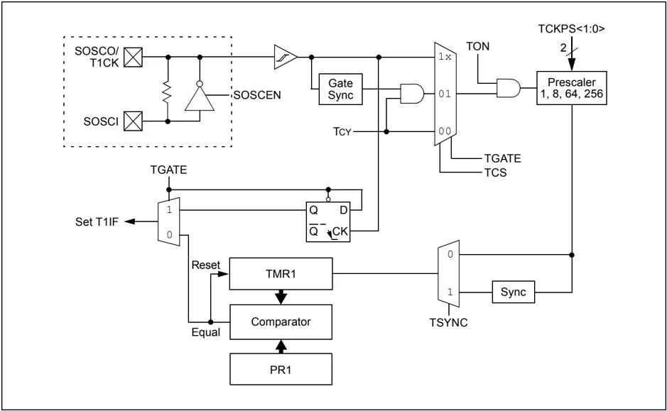
Figure 11-1 presents a block diagram of the 16-bit timer module.
To configure Timer1 for operation:
- Set the TON bit (= 1).
- Select the timer prescaler ratio using the TCKPS<1:0> bits.
- Set the Clock and Gating modes using the TCS and TGATE bits.
- Set or clear the TSYNC bit to configure synchronous or asynchronous operation.
- Load the timer period value into the PR1 register.
- If interrupts are required, set the Timer1 Interrupt Enable bit, T1IE. Use the priority bits, T1IP<2:0>, to set the interrupt priority.
FIGURE 11-1: 16-BIT TIMER1 MODULE BLOCK DIAGRAM
REGISTER 11-1: T1CON: TIMER1 CONTROL REGISTER
| R/W-0 | U-0 | R/W-0 | U-0 | U-0 | U-0 | U-0 | U-0 |
|---|---|---|---|---|---|---|---|
| TON | — | TSIDL | — | — | — | — | — |
| bit 15 | bit 8 |
| U-0 | R/W-0 | R/W-0 | R/W-0 | U-0 | R/W-0 | R/W-0 | U-0 |
|---|---|---|---|---|---|---|---|
| — | TGATE | TCKPS1 | TCKPS0 | — | TSYNC | TCS | — |
| bit 7 | bit 0 |
Legend:
R = Readable bit
W = Writable bit
U = Unimplemented bit, read as ‘0’
-n = Value at POR
‘1’ = Bit is set
‘0’ = Bit is cleared
x = Bit is unknown
bit 15
TON: Timer1 On bit
1 = Starts 16-bit Timer1
0 = Stops 16-bit Timer1
bit 14
Unimplemented: Read as ‘0’
bit 13
TSIDL: Timer1 Stop in Idle Mode bit
1 = Discontinues module operation when device enters Idle mode
0 = Continues module operation in Idle mode
bit 12-7
Unimplemented: Read as ‘0’
bit 6
TGATE: Timer1 Gated Time Accumulation Enable bit
When TCS = 1:
This bit is ignored.
When TCS = 0:
1 = Gated time accumulation is enabled
0 = Gated time accumulation is disabled
bit 5-4
TCKPS<1:0>: Timer1 Input Clock Prescale Select bits
11 = 1:256
10 = 1:64
01 = 1:8
00 = 1:1
bit 3
Unimplemented: Read as ‘0’
bit 2
TSYNC: Timer1 External Clock Input Synchronization Select bit
When TCS = 1:
1 = Synchronizes external clock input
0 = Does not synchronize external clock input
When TCS = 0:
This bit is ignored.
bit 1
TCS: Timer1 Clock Source Select bit
1 = External clock from T1CK pin (on the rising edge)
0 = Internal clock (FOSC/2)
bit 0
Unimplemented: Read as ‘0’