28/44-Pin General Purpose, 16-Bit Flash Microcontrollers
High-Performance CPU
- Modified Harvard Architecture
- Up to 16 MIPS Operation @ 32 MHz
- 8 MHz Internal Oscillator with 4x PLL Option and Multiple Divide Options
- 17-Bit by 17-Bit Single-Cycle Hardware Multiplier
- 32-Bit by 16-Bit Hardware Divider
- 16-Bit x 16-Bit Working Register Array
- C Compiler Optimized Instruction Set Architecture:
- 76 base instructions
- Flexible addressing modes
- Two Address Generation Units (AGUs) for Separate Read and Write Addressing of Data Memory
Special Microcontroller Features
- Operating Voltage Range of 2.0V to 3.6V
- 5.5V Tolerant Input (digital pins only)
- High-Current Sink/Source (18 mA/18 mA) on All I/O Pins
- Flash Program Memory:
- 10,000 erase/write
- 20-year data retention minimum
- Power Management modes:
- Sleep, Idle, Doze and Alternate Clock modes
- Operating current: 650 μA/MIPS, typical at 2.0V
- Sleep current: 150 nA, typical at 2.0V
- Fail-Safe Clock Monitor (FSCM) Operation:
- Detects clock failure and switches to on-chip, low-power RC oscillator
- On-Chip, 2.5V Regulator with Tracking mode
- Power-on Reset (POR), Power-up Timer (PWRT) and Oscillator Start-up Timer (OST)
- Flexible Watchdog Timer (WDT) with On-Chip, Low-Power RC Oscillator for Reliable Operation
- In-Circuit Serial Programming™ (ICSP™) and In-Circuit Debug (ICD) via 2 Pins
- JTAG Boundary Scan Support
Analog Features
- 10-Bit, up to 13-Channel Analog-to-Digital Converter:
- 500 ksps conversion rate
- Conversion available during Sleep and Idle
- Dual Analog Comparators with Programmable Input/Output Configuration
Peripheral Features
- Peripheral Pin Select (PPS):
- Allows independent I/O mapping of many peripherals
- Up to 26 available pins (44-pin devices)
- Continuous hardware integrity checking and safety interlocks prevent unintentional configuration changes
- 8-Bit Parallel Master/Slave Port (PMP/PSP):
- Up to 16-bit multiplexed addressing, with up to 11 dedicated address pins on 44-pin devices
- Programmable polarity on control lines
- Hardware Real-Time Clock/Calendar (RTCC):
- Provides clock, calendar and alarm functions
- Programmable Cyclic Redundancy Check (CRC)
- Two 3-Wire/4-Wire SPI modules (support 4 Frame modes) with 8-Level FIFO Buffer
- Two I²C™ modules Support Multi-Master/Slave mode and 7-Bit/10-Bit Addressing
- Two UART modules:
- Supports RS-485, RS-232, and LIN/J2602
- On-chip hardware encoder/decoder for IrDA®
- Auto-wake-up on Start bit
- Auto-Baud Detect
- 4-level deep FIFO buffer
- Five 16-Bit Timers/Counters with Programmable Prescaler
- Five 16-Bit Capture Inputs
- Five 16-Bit Compare/PWM Outputs
- Configurable Open-Drain Outputs on Digital I/O Pins
- Up to 3 External Interrupt Sources
| Device | Pins | Program Memory (bytes) | SRAM (bytes) | Remappable Pins | Timers 16-Bit | Capture Input | Compare/PWM Output | UART w/ IrDA® | SPI | I²C™ | 10-Bit A/D (ch) | Comparators | PMP/PSP | JTAG |
|---|---|---|---|---|---|---|---|---|---|---|---|---|---|---|
| PIC24FJ16GA002 | 28 | 16K | 4K | 16 | 5 | 5 | 5 | 2 | 2 | 2 | 10 | 2 | Y | Y |
| PIC24FJ32GA002 | 28 | 32K | 8K | 16 | 5 | 5 | 5 | 2 | 2 | 2 | 10 | 2 | Y | Y |
| PIC24FJ48GA002 | 28 | 48K | 8K | 16 | 5 | 5 | 5 | 2 | 2 | 2 | 10 | 2 | Y | Y |
| PIC24FJ64GA002 | 28 | 64K | 8K | 16 | 5 | 5 | 5 | 2 | 2 | 2 | 10 | 2 | Y | Y |
| PIC24FJ16GA004 | 44 | 16K | 4K | 26 | 5 | 5 | 5 | 2 | 2 | 2 | 13 | 2 | Y | Y |
| PIC24FJ32GA004 | 44 | 32K | 8K | 26 | 5 | 5 | 5 | 2 | 2 | 2 | 13 | 2 | Y | Y |
| PIC24FJ48GA004 | 44 | 48K | 8K | 26 | 5 | 5 | 5 | 2 | 2 | 2 | 13 | 2 | Y | Y |
| PIC24FJ64GA004 | 44 | 64K | 8K | 26 | 5 | 5 | 5 | 2 | 2 | 2 | 13 | 2 | Y | Y |

Pin Diagrams
28-Pin SPDIP, SSOP, SOIC
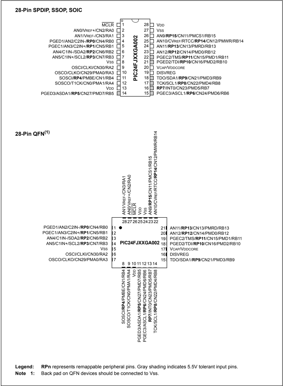
28-Pin QFN(1)
Legend: RPN represents remappable peripheral pins. Gray shading indicates 5.5V tolerant input pins.
Note 1: Back pad on QFN devices should be connected to Vss.
Pin Diagrams (Continued)
44-Pin QFN(1)
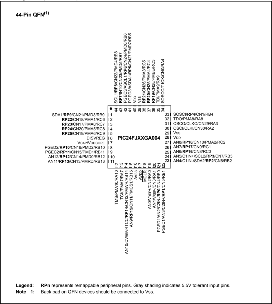
Legend: RPn represents remappable peripheral pins. Gray shading indicates 5.5V tolerant input pins. Note 1: Back pad on QFN devices should be connected to Vss.
Pin Diagrams (Continued)
44-Pin TQFP
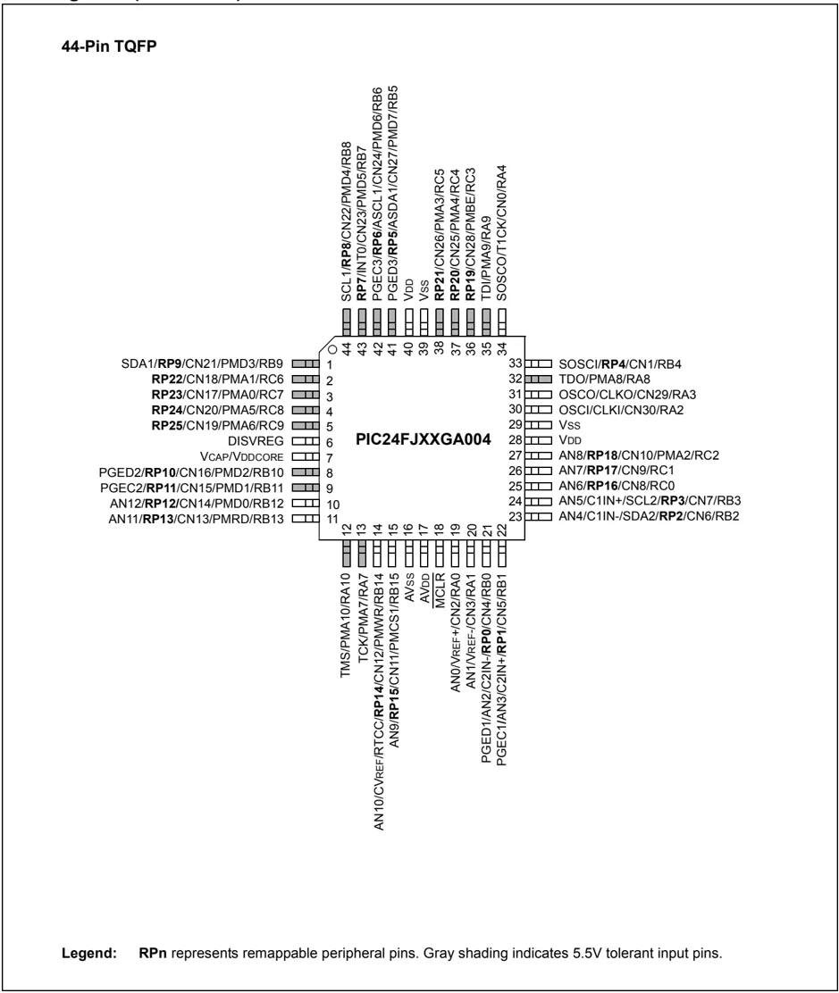
Legend: RPn represents remappable peripheral pins. Gray shading indicates 5.5V tolerant input pins.
DS39881E-page 4 © 2010-2013 Microchip Technology Inc.
Table of Contents
- 1.0 Device Overview ........ 7
- 2.0 Guidelines for Getting Started with 16-Bit Microcontrollers ........ 17
- 3.0 CPU ........ 23
- 4.0 Memory Organization ........ 29
- 5.0 Flash Program Memory ........ 47
- 6.0 Resets ........ 53
- 7.0 Interrupt Controller ........ 59
- 8.0 Oscillator Configuration ........ 95
- 9.0 Power-Saving Features ........ 103
- 10.0 I/O Ports ........ 105
- 11.0 Timer1 ........ 125
- 12.0 Timer2/3 and Timer4/5 ........ 127
- 13.0 Input Capture ........ 133
- 14.0 Output Compare ........ 135
- 15.0 Serial Peripheral Interface (SPI) ........ 141
- 16.0 Inter-Integrated Circuit (I²C™) ........ 151
- 17.0 Universal Asynchronous Receiver Transmitter (UART) ........ 159
- 18.0 Parallel Master Port (PMP) ........ 167
- 19.0 Real-Time Clock and Calendar (RTCC) ........ 177
- 20.0 Programmable Cyclic Redundancy Check (CRC) Generator ........ 189
- 21.0 10-Bit High-Speed A/D Converter ........ 193
- 22.0 Comparator Module ........ 203
- 23.0 Comparator Voltage Reference ........ 207
- 24.0 Special Features ........ 209
- 25.0 Development Support ........ 219
- 26.0 Instruction Set Summary ........ 223
- 27.0 Electrical Characteristics ........ 231
- 28.0 Packaging Information ........ 251
- Appendix A: Revision History ........ 267
- Appendix B: Additional Guidance for PIC24FJ64GA004 Family Applications ........ 268
- Index ........ 269
- The Microchip Web Site ........ 273
- Customer Change Notification Service ........ 273
- Customer Support ........ 273
- Reader Response ........ 274
- Product Identification System ........ 275
TO OUR VALUED CUSTOMERS
It is our intention to provide our valued customers with the best documentation possible to ensure successful use of your Microchip products. To this end, we will continue to improve our publications to better suit your needs. Our publications will be refined and enhanced as new volumes and updates are introduced.
If you have any questions or comments regarding this publication, please contact the Marketing Communications Department via E-mail at docerrors@microchip.com or fax the Reader Response Form in the back of this data sheet to (480) 792-4150. We welcome your feedback.
Most Current Data Sheet
To obtain the most up-to-date version of this data sheet, please register at our Worldwide Web site at: http://www.microchip.com
You can determine the version of a data sheet by examining its literature number found on the bottom outside corner of any page. The last character of the literature number is the version number, (e.g., DS30000A is version A of document DS30000).
Errata
An errata sheet, describing minor operational differences from the data sheet and recommended workarounds, may exist for current devices. As device/documentation issues become known to us, we will publish an errata sheet. The errata will specify the revision of silicon and revision of document to which it applies.
To determine if an errata sheet exists for a particular device, please check with one of the following:
- Microchip’s Worldwide Web site; http://www.microchip.com
- Your local Microchip sales office (see last page)
When contacting a sales office, please specify which device, revision of silicon and data sheet (include literature number) you are using.
Customer Notification System
Register on our web site at www.microchip.com to receive the most current information on all of our products.
DS39881E-page 6 © 2010-2013 Microchip Technology Inc.
1.0 DEVICE OVERVIEW
This document contains device-specific information for the following devices:
- PIC24FJ16GA002
- PIC24FJ32GA002
- PIC24FJ48GA002
- PIC24FJ64GA002
- PIC24FJ16GA004
- PIC24FJ32GA004
- PIC24FJ48GA004
- PIC24FJ64GA004
This family introduces a new line of Microchip devices: a 16-bit microcontroller family with a broad peripheral feature set and enhanced computational performance. The PIC24FJ64GA004 family offers a new migration option for those high-performance applications which may be outgrowing their 8-bit platforms, but don’t require the numerical processing power of a digital signal processor.
1.1 Core Features
1.1.1 16-BIT ARCHITECTURE
Central to all PIC24F devices is the 16-bit modified Harvard architecture, first introduced with Microchip’s dsPIC® Digital Signal Controllers (DSCs). The PIC24F CPU core offers a wide range of enhancements, such as:
- 16-bit data and 24-bit address paths with the ability to move information between data and memory spaces
- Linear addressing of up to 12 Mbytes (program space) and 64 Kbytes (data)
- A 16-element working register array with built-in software stack support
- A 17 x 17 hardware multiplier with support for integer math
- Hardware support for 32 by 16-bit division
- An instruction set that supports multiple addressing modes and is optimized for high-level languages such as ‘C’
- Operational performance up to 16 MIPS
1.1.2 POWER-SAVING TECHNOLOGY
All of the devices in the PIC24FJ64GA004 family incorporate a range of features that can significantly reduce power consumption during operation. Key items include:
- On-the-Fly Clock Switching: The device clock can be changed under software control to the Timer1 source or the internal, low-power RC oscillator during operation, allowing the user to incorporate power-saving ideas into their software designs.
- Doze Mode Operation: When timing-sensitive applications, such as serial communications, require the uninterrupted operation of peripherals, the CPU clock speed can be selectively reduced, allowing incremental power savings without missing a beat.
- Instruction-Based Power-Saving Modes: The microcontroller can suspend all operations, or selectively shut down its core while leaving its peripherals active, with a single instruction in software.
1.1.3 OSCILLATOR OPTIONS AND FEATURES
All of the devices in the PIC24FJ64GA004 family offer five different oscillator options, allowing users a range of choices in developing application hardware. These include:
- Two Crystal modes using crystals or ceramic resonators.
- Two External Clock modes offering the option of a divide-by-2 clock output.
- A Fast Internal Oscillator (FRC) with a nominal 8 MHz output, which can also be divided under software control to provide clock speeds as low as 31 kHz.
- A Phase Lock Loop (PLL) frequency multiplier, available to the External Oscillator modes and the FRC oscillator, which allows clock speeds of up to 32 MHz.
- A separate internal RC oscillator (LPRC) with a fixed 31 kHz output, which provides a low-power option for timing-insensitive applications.
The internal oscillator block also provides a stable reference source for the Fail-Safe Clock Monitor. This option constantly monitors the main clock source against a reference signal provided by the internal oscillator and enables the controller to switch to the internal oscillator, allowing for continued low-speed operation or a safe application shutdown.
1.1.4 EASY MIGRATION
Regardless of the memory size, all devices share the same rich set of peripherals, allowing for a smooth migration path as applications grow and evolve.
The consistent pinout scheme used throughout the entire family also aids in migrating to the next larger device. This is true when moving between devices with the same pin count, or even jumping from 28-pin to 44-pin devices.
The PIC24F family is pin-compatible with devices in the dsPIC33 family, and shares some compatibility with the pinout schema for PIC18 and dsPIC30. This extends the ability of applications to grow from the relatively simple, to the powerful and complex, yet still selecting a Microchip device.
1.2 Other Special Features
- Communications: The PIC24FJ64GA004 family incorporates a range of serial communication peripherals to handle a range of application requirements. There are two independent I²C modules that support both Master and Slave modes of operation. Devices also have, through the Peripheral Pin Select (PPS) feature, two independent UARTs with built-in IrDA encoder/decoders and two SPI modules.
- Peripheral Pin Select (PPS): The Peripheral Pin Select feature allows most digital peripherals to be mapped over a fixed set of digital I/O pins. Users may independently map the input and/or output of any one of the many digital peripherals to any one of the I/O pins.
- Parallel Master/Enhanced Parallel Slave Port: One of the general purpose I/O ports can be reconfigured for enhanced parallel data communications. In this mode, the port can be configured for both master and slave operations, and supports 8-bit and 16-bit data transfers with up to 16 external address lines in Master modes.
- Real-Time Clock/Calendar (RTCC): This module implements a full-featured clock and calendar with alarm functions in hardware, freeing up timer resources and program memory space for use of the core application.
- 10-Bit A/D Converter: This module incorporates programmable acquisition time, allowing for a channel to be selected and a conversion to be initiated without waiting for a sampling period, as well as faster sampling speeds.
1.3 Details on Individual Family Members
Devices in the PIC24FJ64GA004 family are available in 28-pin and 44-pin packages. The general block diagram for all devices is shown in Figure 1-1.
The devices are differentiated from each other in two ways:
- Flash program memory (64 Kbytes for PIC24FJ64GA devices, 48 Kbytes for PIC24FJ48GA devices, 32 Kbytes for PIC24FJ32GA devices and 16 Kbytes for PIC24FJ16GA devices).
- Internal SRAM memory (4k for PIC24FJ16GA devices, 8k for all other devices in the family).
- Available I/O pins and ports (21 pins on 2 ports for 28-pin devices and 35 pins on 3 ports for 44-pin devices).
All other features for devices in this family are identical. These are summarized in Table 1-1.
A list of the pin features that are available on the PIC24FJ64GA004 family devices, sorted by function, is shown in Table 1-2. Note that this table shows the pin location of individual peripheral features and not how they are multiplexed on the same pin. This information is provided in the pinout diagrams in the beginning of the data sheet. Multiplexed features are sorted by the priority given to a feature, with the highest priority peripheral being listed first.
TABLE 1-1: DEVICE FEATURES FOR THE PIC24FJ64GA004 FAMILY
| Features | 16GA002 | 32GA002 | 48GA002 | 64GA002 | 16GA004 | 32GA004 | 48GA004 | 64GA004 |
|---|---|---|---|---|---|---|---|---|
| Operating Frequency | ||||||||
| DC – 32 MHz | ||||||||
| Program Memory (bytes) | 16K | 32K | 48K | 64K | 16K | 32K | 48K | 64K |
| Program Memory (instructions) | 5,504 | 11,008 | 16,512 | 22,016 | 5,504 | 11,008 | 16,512 | 22,016 |
| Data Memory (bytes) | 4096 | 8192 | 4096 | 8192 | ||||
| Interrupt Sources (soft vectors/NMI traps) | ||||||||
| 43 | ||||||||
| (39/4) | ||||||||
| I/O Ports | Ports A, B | Ports A, B, C | ||||||
| Total I/O Pins | 21 | 35 | ||||||
| Timers: | ||||||||
| Total Number (16-bit) | 5⁽¹⁾ | |||||||
| 32-Bit (from paired 16-bit timers) | 2 | |||||||
| Input Capture Channels | 5⁽¹⁾ | |||||||
| Output Compare/PWM Channels | 5⁽¹⁾ | |||||||
| Input Change Notification Interrupt | 21 | 30 | ||||||
| Serial Communications: | ||||||||
| UART | 2⁽¹⁾ | |||||||
| SPI (3-wire/4-wire) | 2⁽¹⁾ | |||||||
| I²C™ | 2 | |||||||
| Parallel Communications (PMP/PSP) | Yes | |||||||
| JTAG Boundary Scan | Yes | |||||||
| 10-Bit Analog-to-Digital Module (input channels) | 10 | 13 | ||||||
| Analog Comparators | 2 | |||||||
| Remappable Pins | 16 | 26 | ||||||
| Resets (and delays) | ||||||||
| POR, BOR, RESET Instruction, MCLR, WDT, Illegal Opcode, REPEAT Instruction, Hardware Traps, Configuration Word Mismatch (PWRT, OST, PLL Lock) | ||||||||
| Instruction Set | 76 Base Instructions, Multiple Addressing Mode Variations | |||||||
| Packages | 28-Pin SPDI□/SSOP/SOIC/QFN | 44-Pin QFN/TQFP |
Note 1: Peripherals are accessible through remappable pins.
FIGURE 1-1: PIC24FJ64GA004 FAMILY GENERAL BLOCK DIAGRAM
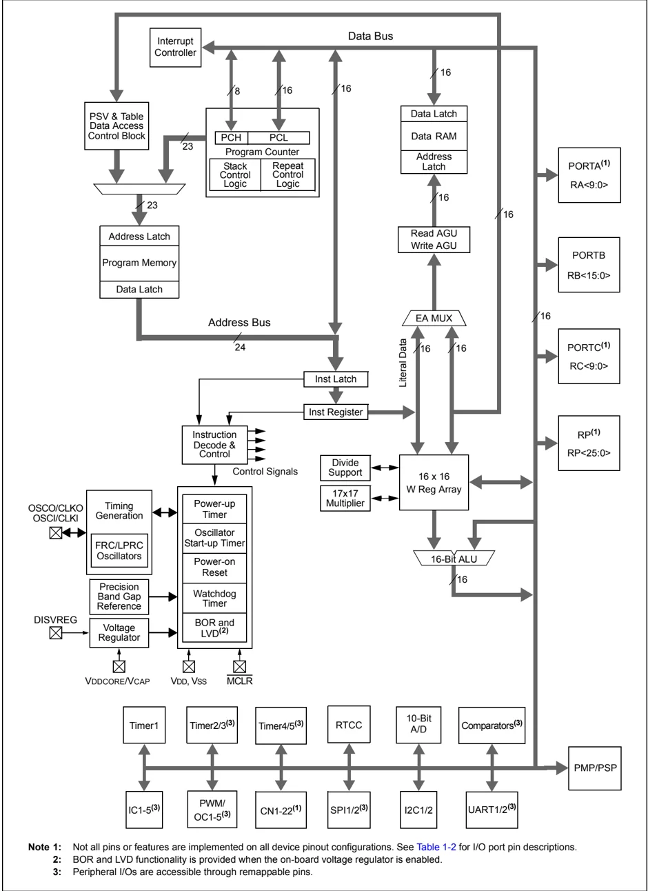
Note 1: Not all pins or features are implemented on all device pinout configurations. See Table 1-2 for I/O port pin descriptions. 2: BOR and LVD functionality is provided when the on-board voltage regulator is enabled. 3: Peripheral I/Os are accessible through remappable pins.
DS39881E-page 10 © 2010-2013 Microchip Technology Inc.
TABLE 1-2: PIC24FJ64GA004 FAMILY PINOUT DESCRIPTIONS
| Function | Pin Number | I/O | Input Buffer | Description | ||
|---|---|---|---|---|---|---|
| 28-Pin SPDIP/ SSOP/SOIC | 28-Pin QFN | 44-Pin QFN/TQFP | ||||
| AN0 | 2 | 27 | 19 | I | ANA | A/D Analog Inputs. |
| AN1 | 3 | 28 | 20 | I | ANA | |
| AN2 | 4 | 1 | 21 | I | ANA | |
| AN3 | 5 | 2 | 22 | I | ANA | |
| AN4 | 6 | 3 | 23 | I | ANA | |
| AN5 | 7 | 4 | 24 | I | ANA | |
| AN6 | — | — | 25 | I | ANA | |
| AN7 | — | — | 26 | I | ANA | |
| AN8 | — | — | 27 | I | ANA | |
| AN9 | 26 | 23 | 15 | I | ANA | |
| AN10 | 25 | 22 | 14 | I | ANA | |
| AN11 | 24 | 21 | 11 | I | ANA | |
| AN12 | 23 | 20 | 10 | I | ANA | |
| ASCL1 | 15 | 12 | 42 | I/O | I²C | Alternate I2C1 Synchronous Serial Clock Input/Output.(1) |
| ASDA1 | 14 | 11 | 41 | I/O | I²C | Alternate I2C2 Synchronous Serial Clock Input/Output.(1) |
| AVDD | — | — | 17 | P | — | Positive Supply for Analog Modules. |
| AVSS | — | — | 16 | P | — | Ground Reference for Analog Modules. |
| C1IN- | 6 | 3 | 23 | I | ANA | Comparator 1 Negative Input. |
| C1IN+ | 7 | 4 | 24 | I | ANA | Comparator 1 Positive Input. |
| C2IN- | 4 | 1 | 21 | I | ANA | Comparator 2 Negative Input. |
| C2IN+ | 5 | 2 | 22 | I | ANA | Comparator 2 Positive Input. |
| CLKI | 9 | 6 | 30 | I | ANA | Main Clock Input Connection. |
| CLKO | 10 | 7 | 31 | O | — | System Clock Output. |
Legend: TTL = TTL input buffer
ANA = Analog level input/output
ST = Schmitt Trigger input buffer
I²C™ = I²C/SMBus input buffer
Note 1: Alternative multiplexing when the I2C1SEL Configuration bit is cleared.
TABLE 1-2: PIC24FJ64GA004 FAMILY PINOUT DESCRIPTIONS (CONTINUED)
| Function | Pin Number | I/O | Input Buffer | Description | ||
|---|---|---|---|---|---|---|
| 28-Pin SPDIP/ SSOP/SOIC | 28-Pin QFN | 44-Pin QFN/TQFP | ||||
| CN0 | 12 | 9 | 34 | I | ST | Interrupt-on-Change Inputs. |
| CN1 | 11 | 8 | 33 | I | ST | |
| CN2 | 2 | 27 | 19 | I | ST | |
| CN3 | 3 | 28 | 20 | I | ST | |
| CN4 | 4 | 1 | 21 | I | ST | |
| CN5 | 5 | 2 | 22 | I | ST | |
| CN6 | 6 | 3 | 23 | I | ST | |
| CN7 | 7 | 4 | 24 | I | ST | |
| CN8 | — | — | 25 | I | ST | |
| CN9 | — | — | 26 | I | ST | |
| CN10 | — | — | 27 | I | ST | |
| CN11 | 26 | 23 | 15 | I | ST | |
| CN12 | 25 | 22 | 14 | I | ST | |
| CN13 | 24 | 21 | 11 | I | ST | |
| CN14 | 23 | 20 | 10 | I | ST | |
| CN15 | 22 | 19 | 9 | I | ST | |
| CN16 | 21 | 18 | 8 | I | ST | |
| CN17 | — | — | 3 | I | ST | |
| CN18 | — | — | 2 | I | ST | |
| CN19 | — | — | 5 | I | ST | |
| CN20 | — | — | 4 | I | ST | |
| CN21 | 18 | 15 | 1 | I | ST | |
| CN22 | 17 | 14 | 44 | I | ST | |
| CN23 | 16 | 13 | 43 | I | ST | |
| CN24 | 15 | 12 | 42 | I | ST | |
| CN25 | — | — | 37 | I | ST | |
| CN26 | — | — | 38 | I | ST | |
| CN27 | 14 | 11 | 41 | I | ST | |
| CN28 | — | — | 36 | I | ST | |
| CN29 | 10 | 7 | 31 | I | ST | |
| CN30 | 9 | 6 | 30 | I | ST | |
| CVREF | 25 | 22 | 14 | O | ANA | Comparator Voltage Reference Output. |
| DISVREG | 19 | 16 | 6 | I | ST | Voltage Regulator Disable. |
| INT0 | 16 | 13 | 43 | I | ST | External Interrupt Input. |
| MCLR | 1 | 26 | 18 | I | ST | Master Clear (device Reset) Input. This line is brought low to cause a Reset. |
Legend: TTL = TTL input buffer ST = Schmitt Trigger input buffer
ANA = Analog level input/output I²C™ = I²C/SMBus input buffer
Note 1: Alternative multiplexing when the I2C1SEL Configuration bit is cleared.
DS39881E-page 12 © 2010-2013 Microchip Technology Inc.
TABLE 1-2: PIC24FJ64GA004 FAMILY PINOUT DESCRIPTIONS (CONTINUED)
| Function | Pin Number | I/O | Input Buffer | Description | ||
|---|---|---|---|---|---|---|
| 28-Pin SPDIP/ SSOP/SOIC | 28-Pin QFN | 44-Pin QFN/TQFP | ||||
| OSCI | 9 | 6 | 30 | I | ANA | Main Oscillator Input Connection. |
| OSCO | 10 | 7 | 31 | O | ANA | Main Oscillator Output Connection. |
| PGEC1 | 5 | 2 | 22 | I/O | ST | In-Circuit Debugger/Emulator and ICSP™ Programming Clock. |
| PGEC2 | 22 | 19 | 9 | I/O | ST | |
| PGEC3 | 14 | 12 | 42 | I/O | ST | |
| PGED1 | 4 | 1 | 21 | I/O | ST | In-Circuit Debugger/Emulator and ICSP Programming Data. |
| PGED2 | 21 | 18 | 8 | I/O | ST | |
| PGED3 | 15 | 11 | 41 | I/O | ST | |
| PMA0 | 10 | 7 | 3 | I/O | ST/TTL | Parallel Master Port Address Bit 0 Input (Buffered Slave modes) and Output (Master modes). |
| PMA1 | 12 | 9 | 2 | I/O | ST/TTL | Parallel Master Port Address Bit 1 Input (Buffered Slave modes) and Output (Master modes). |
| PMA2 | — | — | 27 | O | — | Parallel Master Port Address (Demultiplexed Master modes). |
| PMA3 | — | — | 38 | O | — | |
| PMA4 | — | — | 37 | O | — | |
| PMA5 | — | — | 4 | O | — | |
| PMA6 | — | — | 5 | O | — | |
| PMA7 | — | — | 13 | O | — | |
| PMA8 | — | — | 32 | O | — | |
| PMA9 | — | — | 35 | O | — | |
| PMA10 | — | — | 12 | O | — | |
| PMA11 | — | — | — | O | — | |
| PMA12 | — | — | — | O | — | |
| PMA13 | — | — | — | O | — | |
| PMBE | 11 | 8 | 36 | O | — | Parallel Master Port Byte Enable Strobe. |
| PMCS1 | 26 | 23 | 15 | O | — | Parallel Master Port Chip Select 1 Strobe/Address Bit 14. |
| PMD0 | 23 | 20 | 10 | I/O | ST/TTL | Parallel Master Port Data (Demultiplexed Master mode) or Address/Data (Multiplexed Master modes). |
| PMD1 | 22 | 19 | 9 | I/O | ST/TTL | |
| PMD2 | 21 | 18 | 8 | I/O | ST/TTL | |
| PMD3 | 18 | 15 | 1 | I/O | ST/TTL | |
| PMD4 | 17 | 14 | 44 | I/O | ST/TTL | |
| PMD5 | 16 | 13 | 43 | I/O | ST/TTL | |
| PMD6 | 15 | 12 | 42 | I/O | ST/TTL | |
| PMD7 | 14 | 11 | 41 | I/O | ST/TTL | |
| PMRD | 24 | 21 | 11 | O | — | Parallel Master Port Read Strobe. |
| PMWR | 25 | 22 | 14 | O | — | Parallel Master Port Write Strobe. |
Legend: TTL = TTL input buffer ST = Schmitt Trigger input buffer
ANA = Analog level input/output I²C™ = I²C/SMBus input buffer
Note 1: Alternative multiplexing when the I2C1SEL Configuration bit is cleared.
TABLE 1-2: PIC24FJ64GA004 FAMILY PINOUT DESCRIPTIONS (CONTINUED)
| Function | Pin Number | I/O | Input Buffer | Description | ||
|---|---|---|---|---|---|---|
| 28-Pin SPDIP/ SSOP/SOIC | 28-Pin QFN | 44-Pin QFN/TQFP | ||||
| RA0 | 2 | 27 | 19 | I/O | ST | PORTA Digital I/O. |
| RA1 | 3 | 28 | 20 | I/O | ST | |
| RA2 | 9 | 6 | 30 | I/O | ST | |
| RA3 | 10 | 7 | 31 | I/O | ST | |
| RA4 | 12 | 9 | 34 | I/O | ST | |
| RA7 | — | — | 13 | I/O | ST | |
| RA8 | — | — | 32 | I/O | ST | |
| RA9 | — | — | 35 | I/O | ST | |
| RA10 | — | — | 12 | I/O | ST | |
| RB0 | 4 | 1 | 21 | I/O | ST | PORTB Digital I/O. |
| RB1 | 5 | 2 | 22 | I/O | ST | |
| RB2 | 6 | 3 | 23 | I/O | ST | |
| RB3 | 7 | 4 | 24 | I/O | ST | |
| RB4 | 11 | 8 | 33 | I/O | ST | |
| RB5 | 14 | 11 | 41 | I/O | ST | |
| RB6 | 15 | 12 | 42 | I/O | ST | |
| RB7 | 16 | 13 | 43 | I/O | ST | |
| RB8 | 17 | 14 | 44 | I/O | ST | |
| RB9 | 18 | 15 | 1 | I/O | ST | |
| RB10 | 21 | 18 | 8 | I/O | ST | |
| RB11 | 22 | 19 | 9 | I/O | ST | |
| RB12 | 23 | 20 | 10 | I/O | ST | |
| RB13 | 24 | 21 | 11 | I/O | ST | |
| RB14 | 25 | 22 | 14 | I/O | ST | |
| RB15 | 26 | 23 | 15 | I/O | ST | |
| RC0 | — | — | 25 | I/O | ST | PORTC Digital I/O. |
| RC1 | — | — | 26 | I/O | ST | |
| RC2 | — | — | 27 | I/O | ST | |
| RC3 | — | — | 36 | I/O | ST | |
| RC4 | — | — | 37 | I/O | ST | |
| RC5 | — | — | 38 | I/O | ST | |
| RC6 | — | — | 2 | I/O | ST | |
| RC7 | — | — | 3 | I/O | ST | |
| RC8 | — | — | 4 | I/O | ST | |
| RC9 | — | — | 5 | I/O | ST |
Legend:
TTL = TTL input buffer
ANA = Analog level input/output
ST = Schmitt Trigger input buffer
I²C™ = I²C/SMBus input buffer
Note 1: Alternative multiplexing when the I2C1SEL Configuration bit is cleared.
TABLE 1-2: PIC24FJ64GA004 FAMILY PINOUT DESCRIPTIONS (CONTINUED)
| Function | Pin Number | I/O | Input Buffer | Description | ||
|---|---|---|---|---|---|---|
| 28-Pin SPDIP/ SSOP/SOIC | 28-Pin QFN | 44-Pin QFN/TQFP | ||||
| RP0 | 4 | 1 | 21 | I/O | ST | Remappable Peripheral. |
| RP1 | 5 | 2 | 22 | I/O | ST | |
| RP2 | 6 | 3 | 23 | I/O | ST | |
| RP3 | 7 | 4 | 24 | I/O | ST | |
| RP4 | 11 | 8 | 33 | I/O | ST | |
| RP5 | 14 | 11 | 41 | I/O | ST | |
| RP6 | 15 | 12 | 42 | I/O | ST | |
| RP7 | 16 | 13 | 43 | I/O | ST | |
| RP8 | 17 | 14 | 44 | I/O | ST | |
| RP9 | 18 | 15 | 1 | I/O | ST | |
| RP10 | 21 | 18 | 8 | I/O | ST | |
| RP11 | 22 | 19 | 9 | I/O | ST | |
| RP12 | 23 | 20 | 10 | I/O | ST | |
| RP13 | 24 | 21 | 11 | I/O | ST | |
| RP14 | 25 | 22 | 14 | I/O | ST | |
| RP15 | 26 | 23 | 15 | I/O | ST | |
| RP16 | — | — | 25 | I/O | ST | |
| RP17 | — | — | 26 | I/O | ST | |
| RP18 | — | — | 27 | I/O | ST | |
| RP19 | — | — | 36 | I/O | ST | |
| RP20 | — | — | 37 | I/O | ST | |
| RP21 | — | — | 38 | I/O | ST | |
| RP22 | — | — | 2 | I/O | ST | |
| RP23 | — | — | 3 | I/O | ST | |
| RP24 | — | — | 4 | I/O | ST | |
| RP25 | — | — | 5 | I/O | ST | |
| RTCC | 25 | 22 | 14 | O | — | Real-Time Clock Alarm Output. |
| SCL1 | 17 | 14 | 44 | I/O | I²C | I2C1 Synchronous Serial Clock Input/Output. |
| SCL2 | 7 | 4 | 24 | I/O | I²C | I2C2 Synchronous Serial Clock Input/Output. |
| SDA1 | 18 | 15 | 1 | I/O | I²C | I2C1 Data Input/Output. |
| SDA2 | 6 | 3 | 23 | I/O | I²C | I2C2 Data Input/Output. |
| SOSCI | 11 | 8 | 33 | I | ANA | Secondary Oscillator/Timer1 Clock Input. |
| SOSCO | 12 | 9 | 34 | O | ANA | Secondary Oscillator/Timer1 Clock Output. |
Legend: TTL = TTL input buffer
ANA = Analog level input/output
ST = Schmitt Trigger input buffer
I²C™ = I²C/SMBus input buffer
Note 1: Alternative multiplexing when the I2C1SEL Configuration bit is cleared.
TABLE 1-2: PIC24FJ64GA004 FAMILY PINOUT DESCRIPTIONS (CONTINUED)
| Function | Pin Number | I/O | Input Buffer | Description | ||
|---|---|---|---|---|---|---|
| 28-Pin SPDIP/ SSOP/SOIC | 28-Pin QFN | 44-Pin QFN/TQFP | ||||
| T1CK | 12 | 9 | 34 | I | ST | Timer1 Clock. |
| TCK | 17 | 14 | 13 | I | ST | JTAG Test Clock Input. |
| TDI | 21 | 18 | 35 | I | ST | JTAG Test Data Input. |
| TDO | 18 | 15 | 32 | O | — | JTAG Test Data Output. |
| TMS | 22 | 19 | 12 | I | ST | JTAG Test Mode Select Input. |
| VDD | 13, 28 | 10, 25 | 28, 40 | P | — | Positive Supply for Peripheral Digital Logic and I/O Pins. |
| VDDCAP | 20 | 17 | 7 | P | — | External Filter Capacitor Connection (regulator enabled). |
| VDDCORE | 20 | 17 | 7 | P | — | Positive Supply for Microcontroller Core Logic (regulator disabled). |
| VREF- | 3 | 28 | 20 | I | ANA | A/D and Comparator Reference Voltage (low) Input. |
| VREF+ | 2 | 27 | 19 | I | ANA | A/D and Comparator Reference Voltage (high) Input. |
| VSS | 8, 27 | 5, 24 | 29, 39 | P | — | Ground Reference for Logic and I/O Pins. |
Legend:
TTL = TTL input buffer
ANA = Analog level input/output
ST = Schmitt Trigger input buffer
I²C™ = I²C/SMBus input buffer
Note 1: Alternative multiplexing when the I2C1SEL Configuration bit is cleared.