26.0 INSTRUCTION SET SUMMARY
Note: This chapter is a brief summary of the PIC24F Instruction Set Architecture (ISA) and is not intended to be a comprehensive reference source.
The PIC24F instruction set adds many enhancements to the previous PIC® MCU instruction sets, while maintaining an easy migration from previous PIC MCU instruction sets. Most instructions are a single program memory word. Only three instructions require two program memory locations.
Each single-word instruction is a 24-bit word divided into an 8-bit opcode, which specifies the instruction type and one or more operands, which further specify the operation of the instruction. The instruction set is highly orthogonal and is grouped into four basic categories:
- Word or byte-oriented operations
- Bit-oriented operations
- Literal operations
- Control operations
Table 26-1 shows the general symbols used in describing the instructions. The PIC24F instruction set summary in Table 26-2 lists all the instructions, along with the status flags affected by each instruction.
Most word or byte-oriented W register instructions (including barrel shift instructions) have three operands:
- The first source operand which is typically a register 'Wb' without any address modifier
- The second source operand which is typically a register 'Ws' with or without an address modifier
- The destination of the result which is typically a register 'Wd' with or without an address modifier
However, word or byte-oriented file register instructions have two operands:
- The file register specified by the value, 'f'
- The destination, which could either be the file register 'f' or the W0 register, which is denoted as 'WREG'
Most bit-oriented instructions (including simple rotate/shift instructions) have two operands:
- The W register (with or without an address modifier) or file register (specified by the value of 'Ws' or 'f')
- The bit in the W register or file register (specified by a literal value or indirectly by the contents of register, 'Wb')
The literal instructions that involve data movement may use some of the following operands:
- A literal value to be loaded into a W register or file register (specified by the value of 'k')
- The W register or file register where the literal value is to be loaded (specified by 'Wb' or 'f')
However, literal instructions that involve arithmetic or logical operations use some of the following operands:
- The first source operand which is a register 'Wb' without any address modifier
- The second source operand which is a literal value
- The destination of the result (only if not the same as the first source operand) which is typically a register 'Wd' with or without an address modifier
The control instructions may use some of the following operands:
- A program memory address
- The mode of the table read and table write instructions
All instructions are a single word, except for certain double-word instructions, which were made double-word instructions so that all the required information is available in these 48 bits. In the second word, the 8 MSbs are '0's. If this second word is executed as an instruction (by itself), it will execute as a NOP.
Most single-word instructions are executed in a single instruction cycle, unless a conditional test is true or the Program Counter (PC) is changed as a result of the instruction. In these cases, the execution takes two instruction cycles, with the additional instruction cycle(s) executed as a NOP. Notable exceptions are the BRA (unconditional/computed branch), indirect CALL/GOTO, all table reads and writes, and RETURN/RETFIE instructions, which are single-word instructions but take two or three cycles.
Certain instructions that involve skipping over the subsequent instruction require either two or three cycles if the skip is performed, depending on whether the instruction being skipped is a single-word or two-word instruction. Moreover, double-word moves require two cycles. The double-word instructions execute in two instruction cycles.
TABLE 26-1: SYMBOLS USED IN OPCODE DESCRIPTIONS
| Field | Description |
|---|---|
| #text | Means literal defined by “text” |
| (text) | Means “content of text” |
| [text] | Means “the location addressed by text” |
| { } | Optional field or operation |
| <n:m> | Register bit field |
| .b | Byte mode selection |
| .d | Double-Word mode selection |
| .S | Shadow register select |
| .w | Word mode selection (default) |
| bit4 | 4-bit bit selection field (used in word addressed instructions) ∈ {0...15} |
| C, DC, N, OV, Z | MCU Status bits: Carry, Digit Carry, Negative, Overflow, Sticky Zero |
| Expr | Absolute address, label or expression (resolved by the linker) |
| f | File register address ∈ {0000h...1FFFh} |
| lit1 | 1-bit unsigned literal ∈ {0,1} |
| lit4 | 4-bit unsigned literal ∈ {0...15} |
| lit5 | 5-bit unsigned literal ∈ {0...31} |
| lit8 | 8-bit unsigned literal ∈ {0...255} |
| lit10 | 10-bit unsigned literal ∈ {0...255} for Byte mode, {0:1023} for Word mode |
| lit14 | 14-bit unsigned literal ∈ {0...16384} |
| lit16 | 16-bit unsigned literal ∈ {0...65535} |
| lit23 | 23-bit unsigned literal ∈ {0...8388608}; LSB must be ‘0’ |
| None | Field does not require an entry, may be blank |
| PC | Program Counter |
| Slit10 | 10-bit signed literal ∈ {-512...511} |
| Slit16 | 16-bit signed literal ∈ {-32768...32767} |
| Slit6 | 6-bit signed literal ∈ {-16...16} |
| Wb | Base W register ∈ {W0..W15} |
| Wd | Destination W register ∈ { Wd, [Wd], [Wd++], [Wd--], [++Wd], [--Wd] } |
| Wdo | Destination W register ∈ { Wnd, [Wnd], [Wnd++], [Wnd--], [++Wnd], [--Wnd], [Wnd+Wb] } |
| Wm,Wn | Dividend, Divisor working register pair (direct addressing) |
| Wn | One of 16 working registers ∈ {W0..W15} |
| Wnd | One of 16 destination working registers ∈ {W0..W15} |
| Wns | One of 16 source working registers ∈ {W0..W15} |
| WREG | W0 (working register used in file register instructions) |
| Ws | Source W register ∈ { Ws, [Ws], [Ws++], [Ws--], [++Ws], [--Ws] } |
| Wso | Source W register ∈ { Wns, [Wns], [Wns++], [Wns--], [++Wns], [--Wns], [Wns+Wb] } |
TABLE 26-2: INSTRUCTION SET OVERVIEW
| Assembly Mnemonic | Assembly Syntax | Description | # of Words | # of Cycles | Status Flags Affected |
|---|---|---|---|---|---|
| ADD | ADD f | f = f + WREG | 1 | 1 | C, DC, N, OV, Z |
| ADD f,WREG | WREG = f + WREG | 1 | 1 | C, DC, N, OV, Z | |
| ADD #lit10,Wn | Wd = lit10 + Wd | 1 | 1 | C, DC, N, OV, Z | |
| ADD Wb,Ws,Wd | Wd = Wb + Ws | 1 | 1 | C, DC, N, OV, Z | |
| ADD Wb,#lit5,Wd | Wd = Wb + lit5 | 1 | 1 | C, DC, N, OV, Z | |
| ADDC | ADDC f | f = f + WREG + (C) | 1 | 1 | C, DC, N, OV, Z |
| ADDC f,WREG | WREG = f + WREG + (C) | 1 | 1 | C, DC, N, OV, Z | |
| ADDC #lit10,Wn | Wd = lit10 + Wd + (C) | 1 | 1 | C, DC, N, OV, Z | |
| ADDC Wb,Ws,Wd | Wd = Wb + Ws + (C) | 1 | 1 | C, DC, N, OV, Z | |
| ADDC Wb,#lit5,Wd | Wd = Wb + lit5 + (C) | 1 | 1 | C, DC, N, OV, Z | |
| AND | AND f | f = f .AND. WREG | 1 | 1 | N, Z |
| AND f,WREG | WREG = f .AND. WREG | 1 | 1 | N, Z | |
| AND #lit10,Wn | Wd = lit10 .AND. Wd | 1 | 1 | N, Z | |
| AND Wb,Ws,Wd | Wd = Wb .AND. Ws | 1 | 1 | N, Z | |
| AND Wb,#lit5,Wd | Wd = Wb .AND. lit5 | 1 | 1 | N, Z | |
| ASR | ASR f | f = Arithmetic Right Shift f | 1 | 1 | C, N, OV, Z |
| ASR f,WREG | WREG = Arithmetic Right Shift f | 1 | 1 | C, N, OV, Z | |
| ASR Ws,Wd | Wd = Arithmetic Right Shift Ws | 1 | 1 | C, N, OV, Z | |
| ASR Wb,Wns,Wnd | Wnd = Arithmetic Right Shift Wb by Wns | 1 | 1 | N, Z | |
| ASR Wb,#lit4,Wnd | Wnd = Arithmetic Right Shift Wb by lit4 | 1 | 1 | N, Z | |
| BCLR | BCLR f,#bit4 | Bit Clear f | 1 | 1 | None |
| BCLR Ws,#bit4 | Bit Clear Ws | 1 | 1 | None | |
| BRA | BRA C,Expr | Branch if Carry | 1 | 1 (2) | None |
| BRA GE,Expr | Branch if Greater than or Equal | 1 | 1 (2) | None | |
| BRA GEU,Expr | Branch if Unsigned Greater than or Equal | 1 | 1 (2) | None | |
| BRA GT,Expr | Branch if Greater than | 1 | 1 (2) | None | |
| BRA GTU,Expr | Branch if Unsigned Greater than | 1 | 1 (2) | None | |
| BRA LE,Expr | Branch if Less than or Equal | 1 | 1 (2) | None | |
| BRA LEU,Expr | Branch if Unsigned Less than or Equal | 1 | 1 (2) | None | |
| BRA LT,Expr | Branch if Less than | 1 | 1 (2) | None | |
| BRA LTU,Expr | Branch if Unsigned Less than | 1 | 1 (2) | None | |
| BRA N,Expr | Branch if Negative | 1 | 1 (2) | None | |
| BRA NC,Expr | Branch if Not Carry | 1 | 1 (2) | None | |
| BRA NN,Expr | Branch if Not Negative | 1 | 1 (2) | None | |
| BRA NOV,Expr | Branch if Not Overflow | 1 | 1 (2) | None | |
| BRA NZ,Expr | Branch if Not Zero | 1 | 1 (2) | None | |
| BRA OV,Expr | Branch if Overflow | 1 | 1 (2) | None | |
| BRA Expr | Branch Unconditionally | 1 | 2 | None | |
| BRA Z,Expr | Branch if Zero | 1 | 1 (2) | None | |
| BRA Wn | Computed Branch | 1 | 2 | None | |
| BSET | BSET f,#bit4 | Bit Set f | 1 | 1 | None |
| BSET Ws,#bit4 | Bit Set Ws | 1 | 1 | None | |
| BSW | BSW.C Ws,Wb | Write C bit to Ws<Wb> | 1 | 1 | None |
| BSW.Z Ws,Wb | Write Z bit to Ws<Wb> | 1 | 1 | None | |
| BTG | BTG f,#bit4 | Bit Toggle f | 1 | 1 | None |
| BTG Ws,#bit4 | Bit Toggle Ws | 1 | 1 | None | |
| BTSC | BTSC f,#bit4 | Bit Test f, Skip if Clear | 1 | 1 (2 or 3) | None |
| BTSC Ws,#bit4 | Bit Test Ws, Skip if Clear | 1 | 1 (2 or 3) | None |
TABLE 26-2: INSTRUCTION SET OVERVIEW (CONTINUED)
| Assembly Mnemonic | Assembly Syntax | Description | # of Words | # of Cycles | Status Flags Affected |
|---|---|---|---|---|---|
| BTSS | BTSS f,#bit4 | Bit Test f, Skip if Set | 1 | 1 (2 or 3) | None |
| BTSS Ws,#bit4 | Bit Test Ws, Skip if Set | 1 | 1 (2 or 3) | None | |
| BTST | BTST f,#bit4 | Bit Test f | 1 | 1 | Z |
| BTST.C Ws,#bit4 | Bit Test Ws to C | 1 | 1 | C | |
| BTST.Z Ws,#bit4 | Bit Test Ws to Z | 1 | 1 | Z | |
| BTST.C Ws,Wb | Bit Test Ws<Wb> to C | 1 | 1 | C | |
| BTST.Z Ws,Wb | Bit Test Ws<Wb> to Z | 1 | 1 | Z | |
| BTSTS | BTSTS f,#bit4 | Bit Test then Set f | 1 | 1 | Z |
| BTSTS.C Ws,#bit4 | Bit Test Ws to C, then Set | 1 | 1 | C | |
| BTSTS.Z Ws,#bit4 | Bit Test Ws to Z, then Set | 1 | 1 | Z | |
| CALL | CALL lit23 | Call Subroutine | 2 | 2 | None |
| CALL Wn | Call Indirect Subroutine | 1 | 2 | None | |
| CLR | CLR f | f = 0x0000 | 1 | 1 | None |
| CLR WREG | WREG = 0x0000 | 1 | 1 | None | |
| CLR Ws | Ws = 0x0000 | 1 | 1 | None | |
| CLRWDT | CLRWDT | Clear Watchdog Timer | 1 | 1 | WDTO, Sleep |
| COM | COM f | f = f̅ | 1 | 1 | N, Z |
| COM f,WREG | WREG = f̅ | 1 | 1 | N, Z | |
| COM Ws,Wd | Wd = Ws̅ | 1 | 1 | N, Z | |
| CP | CP f | Compare f with WREG | 1 | 1 | C, DC, N, OV, Z |
| CP Wb,#lit5 | Compare Wb with lit5 | 1 | 1 | C, DC, N, OV, Z | |
| CP Wb,Ws | Compare Wb with Ws (Wb – Ws) | 1 | 1 | C, DC, N, OV, Z | |
| CP0 | CP0 f | Compare f with 0x0000 | 1 | 1 | C, DC, N, OV, Z |
| CP0 Ws | Compare Ws with 0x0000 | 1 | 1 | C, DC, N, OV, Z | |
| CPB | CPB f | Compare f with WREG, with Borrow | 1 | 1 | C, DC, N, OV, Z |
| CPB Wb,#lit5 | Compare Wb with lit5, with Borrow | 1 | 1 | C, DC, N, OV, Z | |
| CPB Wb,Ws | Compare Wb with Ws, with Borrow (Wb – Ws – C̅) | 1 | 1 | C, DC, N, OV, Z | |
| CPSEQ | CPSEQ Wb,Wn | Compare Wb with Wn, Skip if = | 1 | 1 (2 or 3) | None |
| CPSGT | CPSGT Wb,Wn | Compare Wb with Wn, Skip if > | 1 | 1 (2 or 3) | None |
| CPSLT | CPSLT Wb,Wn | Compare Wb with Wn, Skip if < | 1 | 1 (2 or 3) | None |
| CPSNE | CPSNE Wb,Wn | Compare Wb with Wn, Skip if ≠ | 1 | 1 (2 or 3) | None |
| DAW | DAW.B Wn | Wn = Decimal Adjust Wn | 1 | 1 | C |
| DEC | DEC f | f = f – 1 | 1 | 1 | C, DC, N, OV, Z |
| DEC f,WREG | WREG = f – 1 | 1 | 1 | C, DC, N, OV, Z | |
| DEC Ws,Wd | Wd = Ws – 1 | 1 | 1 | C, DC, N, OV, Z | |
| DEC2 | DEC2 f | f = f – 2 | 1 | 1 | C, DC, N, OV, Z |
| DEC2 f,WREG | WREG = f – 2 | 1 | 1 | C, DC, N, OV, Z | |
| DEC2 Ws,Wd | Wd = Ws – 2 | 1 | 1 | C, DC, N, OV, Z | |
| DISI | DISI #lit14 | Disable Interrupts for k Instruction Cycles | 1 | 1 | None |
| DIV | DIV.SW Wm,Wn | Signed 16/16-bit Integer Divide | 1 | 18 | N, Z, C, OV |
| DIV.SD Wm,Wn | Signed 32/16-bit Integer Divide | 1 | 18 | N, Z, C, OV | |
| DIV.UW Wm,Wn | Unsigned 16/16-bit Integer Divide | 1 | 18 | N, Z, C, OV | |
| DIV.UD Wm,Wn | Unsigned 32/16-bit Integer Divide | 1 | 18 | N, Z, C, OV | |
| EXCH | EXCH Wns,Wnd | Swap Wns with Wnd | 1 | 1 | None |
| FBCL | FFBCL Ws,Wnd | Find Bit Change from left (MSb) Side | 1 | 1 | None |
| FF1L | FF1L Ws,Wnd | Find First One from Left (MSb) Side | 1 | 1 | C |
| FF1R | FF1R Ws,Wnd | Find First One from Right (LSb) Side | 1 | 1 | C |
TABLE 26-2: INSTRUCTION SET OVERVIEW (CONTINUED)
| Assembly Mnemonic | Assembly Syntax | Description | # of Words | # of Cycles | Status Flags Affected |
|---|---|---|---|---|---|
| GOTO | GOTO Expr | Go to Address | 2 | 2 | None |
| GOTO Wn | Go to Indirect | 1 | 2 | None | |
| INC | INC f | f = f + 1 | 1 | 1 | C, DC, N, OV, Z |
| INC f,WREG | WREG = f + 1 | 1 | 1 | C, DC, N, OV, Z | |
| INC Ws,Wd | Wd = Ws + 1 | 1 | 1 | C, DC, N, OV, Z | |
| INC2 | INC2 f | f = f + 2 | 1 | 1 | C, DC, N, OV, Z |
| INC2 f,WREG | WREG = f + 2 | 1 | 1 | C, DC, N, OV, Z | |
| INC2 Ws,Wd | Wd = Ws + 2 | 1 | 1 | C, DC, N, OV, Z | |
| IOR | IOR f | f = f .IOR. WREG | 1 | 1 | N, Z |
| IOR f,WREG | WREG = f .IOR. WREG | 1 | 1 | N, Z | |
| IOR #lit10,Wn | Wd = lit10 .IOR. Wd | 1 | 1 | N, Z | |
| IOR Wb,Ws,Wd | Wd = Wb .IOR. Ws | 1 | 1 | N, Z | |
| IOR Wb,#lit5,Wd | Wd = Wb .IOR. lit5 | 1 | 1 | N, Z | |
| LNK | LNK #lit14 | Link Frame Pointer | 1 | 1 | None |
| LSR | LSR f | f = Logical Right Shift f | 1 | 1 | C, N, OV, Z |
| LSR f,WREG | WREG = Logical Right Shift f | 1 | 1 | C, N, OV, Z | |
| LSR Ws,Wd | Wd = Logical Right Shift Ws | 1 | 1 | C, N, OV, Z | |
| LSR Wb,Wns,Wnd | Wnd = Logical Right Shift Wb by Wns | 1 | 1 | N, Z | |
| LSR Wb,#lit4,Wnd | Wnd = Logical Right Shift Wb by lit4 | 1 | 1 | N, Z | |
| MOV | MOV f,Wn | Move f to Wn | 1 | 1 | None |
| MOV [Wns+Slit10],Wnd | Move [Wns+Slit10] to Wnd | 1 | 1 | None | |
| MOV f | Move f to f | 1 | 1 | N, Z | |
| MOV f,WREG | Move f to WREG | 1 | 1 | None | |
| MOV #lit16,Wn | Move 16-bit Literal to Wn | 1 | 1 | None | |
| MOV.b #lit8,Wn | Move 8-bit Literal to Wn | 1 | 1 | None | |
| MOV Wn,f | Move Wn to f | 1 | 1 | None | |
| MOV Wns,[Wns+Slit10] | Move Wns to [Wns+Slit10] | 1 | 1 | None | |
| MOV Wso,Wdo | Move Ws to Wd | 1 | 1 | None | |
| MOV WREG,f | Move WREG to f | 1 | 1 | None | |
| MOV.D Wns,Wd | Move Double from W(ns):W(ns+1) to Wd | 1 | 2 | None | |
| MOV.D Ws,Wnd | Move Double from Ws to W(nd+1):W(nd) | 1 | 2 | None | |
| MUL | MUL.SS Wb,Ws,Wnd | {Wnd+1, Wnd} = Signed(Wb) * Signed(Ws) | 1 | 1 | None |
| MUL.SU Wb,Ws,Wnd | {Wnd+1, Wnd} = Signed(Wb) * Unsigned(Ws) | 1 | 1 | None | |
| MUL.US Wb,Ws,Wnd | {Wnd+1, Wnd} = Unsigned(Wb) * Signed(Ws) | 1 | 1 | None | |
| MUL.UU Wb,Ws,Wnd | {Wnd+1, Wnd} = Unsigned(Wb) * Unsigned(Ws) | 1 | 1 | None | |
| MUL.SU Wb,#lit5,Wnd | {Wnd+1, Wnd} = Signed(Wb) * Unsigned(lit5) | 1 | 1 | None | |
| MUL.UU Wb,#lit5,Wnd | {Wnd+1, Wnd} = Unsigned(Wb) * Unsigned(lit5) | 1 | 1 | None | |
| MUL f | W3:W2 = f * WREG | 1 | 1 | None | |
| NEG | NEG f | f = f̅ + 1 | 1 | 1 | C, DC, N, OV, Z |
| NEG f,WREG | WREG = f̅ + 1 | 1 | 1 | C, DC, N, OV, Z | |
| NEG Ws,Wd | Wd = Ws̅ + 1 | 1 | 1 | C, DC, N, OV, Z | |
| NOP | NOP | No Operation | 1 | 1 | None |
| NOPR | No Operation | 1 | 1 | None | |
| POP | POP f | Pop f from Top-of-Stack (TOS) | 1 | 1 | None |
| POP Wdo | Pop from Top-of-Stack (TOS) to Wdo | 1 | 1 | None | |
| POP.D Wnd | Pop from Top-of-Stack (TOS) to W(nd):W(nd+1) | 1 | 2 | None | |
| POP.S | Pop Shadow Registers | 1 | 1 | All | |
| PUSH | PUSH f | Push f to Top-of-Stack (TOS) | 1 | 1 | None |
| PUSH Wso | Push Wso to Top-of-Stack (TOS) | 1 | 1 | None | |
| PUSH.D Wns | Push W(ns):W(ns+1) to Top-of-Stack (TOS) | 1 | 2 | None | |
| PUSH.S | Push Shadow Registers | 1 | 1 | None |
TABLE 26-2: INSTRUCTION SET OVERVIEW (CONTINUED)
| Assembly Mnemonic | Assembly Syntax | Description | # of Words | # of Cycles | Status Flags Affected |
|---|---|---|---|---|---|
| PWRSAV | PWRSAV #lit1 | Go into Sleep or Idle mode | 1 | 1 | WDTO, Sleep |
| RCALL | RCALL Expr | Relative Call | 1 | 2 | None |
| RCALL Wn | Computed Call | 1 | 2 | None | |
| REPEAT | REPEAT #lit14 | Repeat Next Instruction lit14 + 1 times | 1 | 1 | None |
| REPEAT Wn | Repeat Next Instruction (Wn) + 1 times | 1 | 1 | None | |
| RESET | RESET | Software Device Reset | 1 | 1 | None |
| RETFIE | RETFIE | Return from Interrupt | 1 | 3 (2) | None |
| RETLW | RETLW #lit10,Wn | Return with Literal in Wn | 1 | 3 (2) | None |
| RETURN | RETURN | Return from Subroutine | 1 | 3 (2) | None |
| RLC | RLC f | f = Rotate Left through Carry f | 1 | 1 | C, N, Z |
| RLC f,WREG | WREG = Rotate Left through Carry f | 1 | 1 | C, N, Z | |
| RLC Ws,Wd | Wd = Rotate Left through Carry Ws | 1 | 1 | C, N, Z | |
| RLNC | RLNC f | f = Rotate Left (No Carry) f | 1 | 1 | N, Z |
| RLNC f,WREG | WREG = Rotate Left (No Carry) f | 1 | 1 | N, Z | |
| RLNC Ws,Wd | Wd = Rotate Left (No Carry) Ws | 1 | 1 | N, Z | |
| RRC | RRC f | f = Rotate Right through Carry f | 1 | 1 | C, N, Z |
| RRC f,WREG | WREG = Rotate Right through Carry f | 1 | 1 | C, N, Z | |
| RRC Ws,Wd | Wd = Rotate Right through Carry Ws | 1 | 1 | C, N, Z | |
| RRNC | RRNC f | f = Rotate Right (No Carry) f | 1 | 1 | N, Z |
| RRNC f,WREG | WREG = Rotate Right (No Carry) f | 1 | 1 | N, Z | |
| RRNC Ws,Wd | Wd = Rotate Right (No Carry) Ws | 1 | 1 | N, Z | |
| SE | SE Ws,Wnd | Wnd = Sign-Extended Ws | 1 | 1 | C, N, Z |
| SETM | SETM f | f = FFFFh | 1 | 1 | None |
| SETM WREG | WREG = FFFFh | 1 | 1 | None | |
| SETM Ws | Ws = FFFFh | 1 | 1 | None | |
| SL | SL f | f = Left Shift f | 1 | 1 | C, N, OV, Z |
| SL f,WREG | WREG = Left Shift f | 1 | 1 | C, N, OV, Z | |
| SL Ws,Wd | Wd = Left Shift Ws | 1 | 1 | C, N, OV, Z | |
| SL Wb,Wns,Wnd | Wnd = Left Shift Wb by Wns | 1 | 1 | N, Z | |
| SL Wb,#lit4,Wnd | Wnd = Left Shift Wb by lit4 | 1 | 1 | N, Z | |
| SUB | SUB f | f = f – WREG | 1 | 1 | C, DC, N, OV, Z |
| SUB f,WREG | WREG = f – WREG | 1 | 1 | C, DC, N, OV, Z | |
| SUB #lit10,Wn | Wn = Wn – lit10 | 1 | 1 | C, DC, N, OV, Z | |
| SUB Wb,Ws,Wd | Wd = Wb – Ws | 1 | 1 | C, DC, N, OV, Z | |
| SUB Wb,#lit5,Wd | Wd = Wb – lit5 | 1 | 1 | C, DC, N, OV, Z | |
| SUBB | SUBB f | f = f – WREG – (C̅) | 1 | 1 | C, DC, N, OV, Z |
| SUBB f,WREG | WREG = f – WREG – (C̅) | 1 | 1 | C, DC, N, OV, Z | |
| SUBB #lit10,Wn | Wn = Wn – lit10 – (C̅) | 1 | 1 | C, DC, N, OV, Z | |
| SUBB Wb,Ws,Wd | Wd = Wb – Ws – (C̅) | 1 | 1 | C, DC, N, OV, Z | |
| SUBB Wb,#lit5,Wd | Wd = Wb – lit5 – (C̅) | 1 | 1 | C, DC, N, OV, Z | |
| SUBR | SUBR f | f = WREG – f | 1 | 1 | C, DC, N, OV, Z |
| SUBR f,WREG | WREG = WREG – f | 1 | 1 | C, DC, N, OV, Z | |
| SUBR Wb,Ws,Wd | Wd = Ws – Wb | 1 | 1 | C, DC, N, OV, Z | |
| SUBR Wb,#lit5,Wd | Wd = lit5 – Wb | 1 | 1 | C, DC, N, OV, Z | |
| SUBBR | SUBBR f | f = WREG – f – (C̅) | 1 | 1 | C, DC, N, OV, Z |
| SUBBR f,WREG | WREG = WREG – f – (C̅) | 1 | 1 | C, DC, N, OV, Z | |
| SUBBR Wb,Ws,Wd | Wd = Ws – Wb – (C̅) | 1 | 1 | C, DC, N, OV, Z | |
| SUBBR Wb,#lit5,Wd | Wd = lit5 – Wb – (C̅) | 1 | 1 | C, DC, N, OV, Z | |
| SWAP | SWAP.b Wn | Wn = Nibble Swap Wn | 1 | 1 | None |
| SWAP Wn | Wn = Byte Swap Wn | 1 | 1 | None |
TABLE 26-2: INSTRUCTION SET OVERVIEW (CONTINUED)
| Assembly Mnemonic | Assembly Syntax | Description | # of Words | # of Cycles | Status Flags Affected |
|---|---|---|---|---|---|
| TBLRDH | TBLRDH Ws,Wd | Read Prog<23:16> to Wd<7:0> | 1 | 2 | None |
| TBLRDL | TBLRDL Ws,Wd | Read Prog<15:0> to Wd | 1 | 2 | None |
| TBLWTH | TBLWTH Ws,Wd | Write Ws<7:0> to Prog<23:16> | 1 | 2 | None |
| TBLWTL | TBLWTL Ws,Wd | Write Ws to Prog<15:0> | 1 | 2 | None |
| ULNK | ULNK | Unlink Frame Pointer | 1 | 1 | None |
| XOR | XOR f | f = f .XOR. WREG | 1 | 1 | N, Z |
| XOR f,WREG | WREG = f .XOR. WREG | 1 | 1 | N, Z | |
| XOR #lit10,Wn | Wd = lit10 .XOR. Wd | 1 | 1 | N, Z | |
| XOR Wb,Ws,Wd | Wd = Wb .XOR. Ws | 1 | 1 | N, Z | |
| XOR Wb,#lit5,Wd | Wd = Wb .XOR. lit5 | 1 | 1 | N, Z | |
| ZE | ZE Ws,Wnd | Wnd = Zero-Extend Ws | 1 | 1 | C, Z, N |
NOTES:
27.0 ELECTRICAL CHARACTERISTICS
This section provides an overview of the PIC24FJ64GA004 family electrical characteristics. Additional information will be provided in future revisions of this document as it becomes available.
Absolute maximum ratings for the PIC24FJ64GA004 family are listed below. Exposure to these maximum rating conditions for extended periods may affect device reliability. Functional operation of the device at these, or any other conditions above the parameters indicated in the operation listings of this specification, is not implied.
Absolute Maximum Ratings(†)
- Ambient temperature under bias ........ -40°C to +135°C
- Storage temperature ........ -65°C to +150°C
- Voltage on VDD with respect to VSS ........ -0.3V to +4.0V
- Voltage on any combined analog and digital pin and MCLR, with respect to VSS ........ -0.3V to (VDD + 0.3V)
- Voltage on any digital only pin with respect to VSS ........ -0.3V to +6.0V
- Voltage on VDDCORE with respect to VSS ........ -0.3V to +3.0V
- Maximum current out of VSS pin ........ 300 mA
- Maximum current into VDD pin (Note 1) ........ 250 mA
- Maximum output current sunk by any I/O pin ........ 25 mA
- Maximum output current sourced by any I/O pin ........ 25 mA
- Maximum current sunk by all ports ........ 200 mA
- Maximum current sourced by all ports (Note 1) ........ 200 mA
Note 1: Maximum allowable current is a function of device maximum power dissipation (see Table 27-1).
† NOTICE: Stresses above those listed under “Absolute Maximum Ratings” may cause permanent damage to the device. This is a stress rating only and functional operation of the device at those or any other conditions above those indicated in the operation listings of this specification is not implied. Exposure to maximum rating conditions for extended periods may affect device reliability.
27.1 DC Characteristics
FIGURE 27-1: PIC24FJ64GA004 FAMILY VOLTAGE-FREQUENCY GRAPH (INDUSTRIAL)
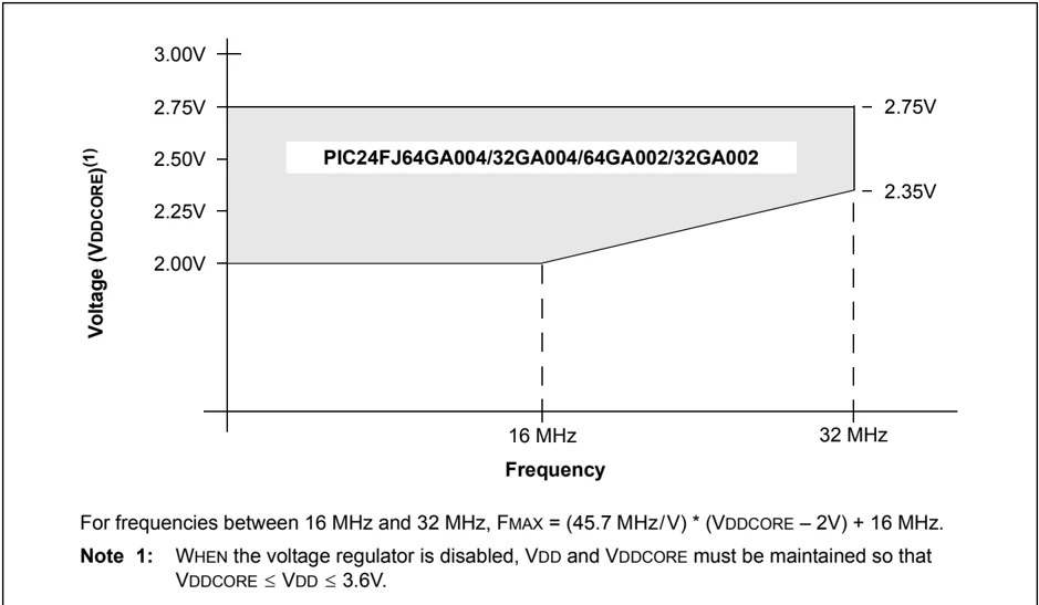
For frequencies between 16 MHz and 32 MHz, FMAX = (45.7 MHz/V) * (VDDCORE – 2V) + 16 MHz. Note 1: WHEN the voltage regulator is disabled, VDD and VDDCORE must be maintained so that VDDCORE ≤ VDD ≤ 3.6V.
FIGURE 27-2: PIC24FJ64GA004 FAMILY VOLTAGE-FREQUENCY GRAPH (EXTENDED TEMPERATURE)
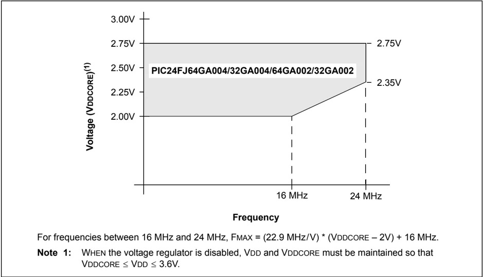
For frequencies between 16 MHz and 24 MHz, FMAX = (22.9 MHz/V) * (VDDCORE – 2V) + 16 MHz. Note 1: WHEN the voltage regulator is disabled, VDD and VDDCORE must be maintained so that VDDCORE ≤ VDD ≤ 3.6V.
DS39881E-page 232 © 2010-2013 Microchip Technology Inc.
TABLE 27-1: THERMAL OPERATING CONDITIONS
| Rating | Symbol | Min | Typ | Max | Unit |
|---|---|---|---|---|---|
| PIC24FJ64GA004 Family: | |||||
| Operating Junction Temperature Range | TJ | -40 | — | +140 | °C |
| Operating Ambient Temperature Range | TA | -40 | — | +125 | °C |
| Power Dissipation: | |||||
| Internal Chip Power Dissipation: PINT = VDD x (IDD – Σ IOH) | PD | PINT + PI/O | W | ||
| I/O Pin Power Dissipation: PI/O = Σ ({VDD – VOH} x IOH) + Σ (VOL x IOL) | |||||
| Maximum Allowed Power Dissipation | PDMAX | (TJ – TA)/θJA | W |
TABLE 27-2: THERMAL PACKAGING CHARACTERISTICS
| Characteristic | Symbol | Typ | Max | Unit | Notes |
|---|---|---|---|---|---|
| Package Thermal Resistance, 300 mil SOIC | θJA | 49 | — | °C/W | (Note 1) |
| Package Thermal Resistance, 6x6x0.9 mm QFN | θJA | 33.7 | — | °C/W | (Note 1) |
| Package Thermal Resistance, 8x8x1 mm QFN | θJA | 28 | — | °C/W | (Note 1) |
| Package Thermal Resistance, 10x10x1 mm TQFP | θJA | 39.3 | — | °C/W | (Note 1) |
Note 1: Junction to ambient thermal resistance; Theta-JA (θJA) numbers are achieved by package simulations.
TABLE 27-3: DC CHARACTERISTICS: TEMPERATURE AND VOLTAGE SPECIFICATIONS
| DC CHARACTERISTICS | Standard Operating Conditions: 2.0V to 3.6V (unless otherwise stated) Operating temperature -40°C ≤ TA ≤ +85°C for Industrial -40°C ≤ TA ≤ +125°C for Extended | ||||||
|---|---|---|---|---|---|---|---|
| Param No. | Symbol | Characteristic | Min | Typ(1) | Max | Units | Conditions |
| Operating Voltage | |||||||
| DC10 | Supply Voltage | ||||||
| VDD | VBORMIN | — | 3.6 | V | Regulator enabled | ||
| VDD | VDDCORE | — | 3.6 | V | Regulator disabled | ||
| VDDCORE | 2.0 | — | 2.75 | V | Regulator disabled | ||
| DC12 | VDR | RAM Data Retention Voltage(2) | 1.5 | — | — | V | |
| DC16 | VPOR | Vdd Start Voltage to Ensure Internal Power-on Reset Signal | — | — | VSS | V | |
| DC17 | SVDD | Vdd Rise Rate to Ensure Internal Power-on Reset Signal | 0.05 | — | — | V/ms | 0-3.3V in 0.1s 0-2.5V in 60 ms |
| DC18 | VBOR | Brown-out Reset Voltage | 1.8 | 2.1 | 2.2 | V |
Note 1: Data in “Typ” column is at 3.3V, +25°C unless otherwise stated. Parameters are for design guidance only and are not tested.
2: This is the limit to which VDD can be lowered without losing RAM data.
TABLE 27-4: DC CHARACTERISTICS: OPERATING CURRENT (IDD)
DC CHARACTERISTICS
Standard Operating Conditions: 2.0V to 3.6V (unless otherwise stated)
Operating temperature
-40°C ≤ TA ≤ +85°C for Industrial
-40°C ≤ TA ≤ +125°C for Extended
| Parameter No. | Typical⁽¹⁾ | Max | Units | Conditions | ||
|---|---|---|---|---|---|---|
| Operating Current (IDD): PMD Bits are Set⁽²⁾ | ||||||
| DC20 | 0.650 | 0.850 | mA | -40°C | 2.0V⁽³⁾ | 1 MIPS |
| DC20a | 0.650 | 0.850 | mA | +25°C | ||
| DC20b | 0.650 | 0.850 | mA | +85°C | ||
| DC20c | 0.650 | 0.850 | mA | +125°C | ||
| DC20d | 1.2 | 1.6 | mA | -40°C | 3.3V⁽⁴⁾ | |
| DC20e | 1.2 | 1.6 | mA | +25°C | ||
| DC20f | 1.2 | 1.6 | mA | +85°C | ||
| DC20g | 1.2 | 1.6 | mA | +125°C | ||
| DC23 | 2.6 | 3.4 | mA | -40°C | 2.0V⁽³⁾ | 4 MIPS |
| DC23a | 2.6 | 3.4 | mA | +25°C | ||
| DC23b | 2.6 | 3.4 | mA | +85°C | ||
| DC23c | 2.6 | 3.4 | mA | +125°C | ||
| DC23d | 4.1 | 5.4 | mA | -40°C | 3.3V⁽⁴⁾ | |
| DC23e | 4.1 | 5.4 | mA | +25°C | ||
| DC23f | 4.1 | 5.4 | mA | +85°C | ||
| DC23g | 4.1 | 5.4 | mA | +125°C | ||
| DC24 | 13.5 | 17.6 | mA | -40°C | 2.5V⁽³⁾ | 16 MIPS |
| DC24a | 13.5 | 17.6 | mA | +25°C | ||
| DC24b | 13.5 | 17.6 | mA | +85°C | ||
| DC24c | 13.5 | 17.6 | mA | +125°C | ||
| DC24d | 15 | 20 | mA | -40°C | 3.3V⁽⁴⁾ | |
| DC24e | 15 | 20 | mA | +25°C | ||
| DC24f | 15 | 20 | mA | +85°C | ||
| DC24g | 15 | 20 | mA | +125°C | ||
| DC31 | 13 | 17 | μA | -40°C | 2.0V⁽³⁾ | LPRC (31 kHz) |
| DC31a | 13 | 17 | μA | +25°C | ||
| DC31b | 20 | 26 | μA | +85°C | ||
| DC31c | 40 | 50 | μA | +125°C | ||
| DC31d | 54 | 70 | μA | -40°C | 3.3V⁽⁴⁾ | |
| DC31e | 54 | 70 | μA | +25°C | ||
| DC31f | 95 | 124 | μA | +85°C | ||
| DC31g | 120 | 260 | μA | +125°C |
Note 1: Data in “Typical” column is at 3.3V, +25°C unless otherwise stated. Parameters are for design guidance only and are not tested.
2: The supply current is mainly a function of the operating voltage and frequency. Other factors, such as I/O pin loading and switching rate, oscillator type, internal code execution pattern and temperature, also have an impact on the current consumption. The test conditions for all IDD measurements are as follows: OSC1 driven with external square wave from rail-to-rail. All I/O pins are configured as inputs and pulled to VDD.
MCLR = VDD; WDT and FSCM are disabled. CPU, SRAM, program memory and data memory are operational. No peripheral modules are operating and all of the Peripheral Module Disable (PMD) bits are set.
3: On-chip voltage regulator is disabled (DISVREG tied to VDD).
4: On-chip voltage regulator is enabled (DISVREG tied to VSS). Low-Voltage Detect (LVD) and Brown-out Detect (BOD) are enabled.
TABLE 27-5: DC CHARACTERISTICS: IDLE CURRENT (IIDLE)
DC CHARACTERISTICS
Standard Operating Conditions: 2.0V to 3.6V (unless otherwise stated)
Operating temperature
-40°C ≤ TA ≤ +85°C for Industrial
-40°C ≤ TA ≤ +125°C for Extended
| Parameter No. | Typical(1) | Max | Units | Conditions | ||
|---|---|---|---|---|---|---|
| Idle Current (IIDLE): Core Off, Clock On Base Current, PMD Bits are Set(2) | ||||||
| DC40 | 150 | 200 | μA | -40°C | 2.0V(3) | 1 MIPS |
| DC40a | 150 | 200 | μA | +25°C | ||
| DC40b | 150 | 200 | μA | +85°C | ||
| DC40c | 165 | 220 | μA | +125°C | ||
| DC40d | 250 | 325 | μA | -40°C | 3.3V(4) | |
| DC40e | 250 | 325 | μA | +25°C | ||
| DC40f | 250 | 325 | μA | +85°C | ||
| DC40g | 275 | 360 | μA | +125°C | ||
| DC43 | 0.55 | 0.72 | mA | -40°C | 2.0V(3) | 4 MIPS |
| DC43a | 0.55 | 0.72 | mA | +25°C | ||
| DC43b | 0.55 | 0.72 | mA | +85°C | ||
| DC43c | 0.60 | 0.8 | mA | +125°C | ||
| DC43d | 0.82 | 1.1 | mA | -40°C | 3.3V(4) | |
| DC43e | 0.82 | 1.1 | mA | +25°C | ||
| DC43f | 0.82 | 1.1 | mA | +85°C | ||
| DC43g | 0.91 | 1.2 | mA | +125°C | ||
| DC47 | 3 | 4 | mA | -40°C | 2.5V(3) | 16 MIPS |
| DC47a | 3 | 4 | mA | +25°C | ||
| DC47b | 3 | 4 | mA | +85°C | ||
| DC47c | 3.3 | 4.4 | mA | +125°C | ||
| DC47d | 3.5 | 4.6 | mA | -40°C | 3.3V(4) | |
| DC47e | 3.5 | 4.6 | mA | +25°C | ||
| DC47f | 3.5 | 4.6 | mA | +85°C | ||
| DC47g | 3.9 | 5.1 | mA | +125°C | ||
| DC50 | 0.85 | 1.1 | mA | -40°C | 2.0V(3) | FRC (4 MIPS) |
| DC50a | 0.85 | 1.1 | mA | +25°C | ||
| DC50b | 0.85 | 1.1 | mA | +85°C | ||
| DC50c | 0.94 | 1.2 | mA | +125°C | ||
| DC50d | 1.2 | 1.6 | mA | -40°C | 3.3V(4) | |
| DC50e | 1.2 | 1.6 | mA | +25°C | ||
| DC50f | 1.2 | 1.6 | mA | +85°C | ||
| DC50g | 1.3 | 1.8 | mA | +125°C |
Note 1: Data in “Typical” column is at 3.3V, +25°C unless otherwise stated. Parameters are for design guidance only and are not tested.
2: The test conditions for all IIDLE measurements are as follows: OSCI driven with external square wave from rail-to-rail. All I/O pins are configured as inputs and pulled to VDD. MCLR = VDD; WDT and FSCM are disabled. CPU, SRAM, program memory and data memory are operational. No peripheral modules are operating and all of the Peripheral Module Disable (PMD) bits are set.
3: On-chip voltage regulator is disabled (DISVREG tied to VDD).
4: On-chip voltage regulator is enabled (DISVREG tied to VSS). Low-Voltage Detect (LVD) and Brown-out Detect (BOD) are enabled.
TABLE 27-5: DC CHARACTERISTICS: IDLE CURRENT (IIdle) (CONTINUED)
| DC CHARACTERISTICS | Standard Operating Conditions: 2.0V to 3.6V (unless otherwise stated) Operating temperature -40°C ≤ TA ≤ +85°C for Industrial -40°C ≤ TA ≤ +125°C for Extended | |||||
|---|---|---|---|---|---|---|
| Parameter No. | Typical(1) | Max | Units | Conditions | ||
| Idle Current (IIdle): Core Off, Clock On Base Current, PMD Bits are Set(2) | ||||||
| DC51 | 4 | 6 | μA | -40°C | 2.0V(3) | LPRC (31 kHz) |
| DC51a | 4 | 6 | μA | +25°C | ||
| DC51b | 8 | 16 | μA | +85°C | ||
| DC51c | 20 | 50 | μA | +125°C | ||
| DC51d | 42 | 55 | μA | -40°C | 3.3V(4) | |
| DC51e | 42 | 55 | μA | +25°C | ||
| DC51f | 70 | 91 | μA | +85°C | ||
| DC51g | 100 | 180 | μA | +125°C |
Note 1: Data in “Typical” column is at 3.3V, +25°C unless otherwise stated. Parameters are for design guidance only and are not tested.
2: The test conditions for all IIdle measurements are as follows: OSC1 driven with external square wave from rail-to-rail. All I/O pins are configured as inputs and pulled to VDD. MCLR = VDD; WDT and FSCM are disabled. CPU, SRAM, program memory and data memory are operational. No peripheral modules are operating and all of the Peripheral Module Disable (PMD) bits are set.
3: On-chip voltage regulator is disabled (DISVREG tied to VDD).
4: On-chip voltage regulator is enabled (DISVREG tied to VSS). Low-Voltage Detect (LVD) and Brown-out Detect (BOD) are enabled.
TABLE 27-6: DC CHARACTERISTICS: POWER-DOWN CURRENT (IPD)
| DC CHARACTERISTICS | Standard Operating Conditions: 2.0V to 3.6V (unless otherwise stated) Operating temperature -40°C ≤ TA ≤ +85°C for Industrial -40°C ≤ TA ≤ +125°C for Extended | |||||
|---|---|---|---|---|---|---|
| Parameter No. | Typical(1) | Max | Units | Conditions | ||
| Power-Down Current (IPD): PMD Bits are Set, PMSLP Bit is ‘0’(2) | ||||||
| DC60 | 0.1 | 1 | μA | -40°C | 2.0V(3) | Base Power-Down Current(5) |
| DC60a | 0.15 | 1 | μA | +25°C | ||
| DC60m | 2.2 | 7.4 | μA | +60°C | ||
| DC60b | 3.7 | 12 | μA | +85°C | ||
| DC60j | 15 | 50 | μA | +125°C | ||
| DC60c | 0.2 | 1 | μA | -40°C | 2.5V(3) | |
| DC60d | 0.25 | 1 | μA | +25°C | ||
| DC60n | 2.6 | 15 | μA | +60°C | ||
| DC60e | 4.2 | 25 | μA | +85°C | ||
| DC60k | 16 | 100 | μA | +125°C | ||
| DC60f | 3.3 | 9 | μA | -40°C | 3.3V(4) | |
| DC60g | 3.5 | 10 | μA | +25°C | ||
| DC60o | 6.7 | 22 | μA | +60°C | ||
| DC60h | 9 | 30 | μA | +85°C | ||
| DC60l | 36 | 120 | μA | +125°C | ||
| DC61 | 1.75 | 3 | μA | -40°C | 2.0V(3) | Watchdog Timer Current: ΔIWDT(5) |
| DC61a | 1.75 | 3 | μA | +25°C | ||
| DC61m | 1.75 | 3 | μA | +60°C | ||
| DC61b | 1.75 | 3 | μA | +85°C | ||
| DC61j | 3.5 | 6 | μA | +125°C | ||
| DC61c | 2.4 | 4 | μA | -40°C | 2.5V(3) | |
| DC61d | 2.4 | 4 | μA | +25°C | ||
| DC61n | 2.4 | 4 | μA | +60°C | ||
| DC61e | 2.4 | 4 | μA | +85°C | ||
| DC61k | 4.8 | 8 | μA | +125°C | ||
| DC61f | 2.8 | 5 | μA | -40°C | 3.3V(4) | |
| DC61g | 2.8 | 5 | μA | +25°C | ||
| DC61o | 2.8 | 5 | μA | +60°C | ||
| DC61h | 2.8 | 5 | μA | +85°C | ||
| DC61l | 5.6 | 10 | μA | +125°C |
Note 1: Data in the Typical column is at 3.3V, +25°C unless otherwise stated. Parameters are for design guidance only and are not tested.
2: Base IPD is measured with all peripherals and clocks shut down. All I/Os are configured as inputs and pulled high. WDT, etc., are all switched off.
3: On-chip voltage regulator is disabled (DISVREG tied to VDD).
4: On-chip voltage regulator is enabled (DISVREG tied to VSS). Low-Voltage Detect (LVD) and Brown-out Detect (BOD) are enabled.
5: The Δ current is the additional current consumed when the module is enabled. This current should be added to the base IPD current.
DS39881E-page 238 © 2010-2013 Microchip Technology Inc.
TABLE 27-6: DC CHARACTERISTICS: POWER-DOWN CURRENT (IPD) (CONTINUED)
DC CHARACTERISTICS
Standard Operating Conditions: 2.0V to 3.6V (unless otherwise stated)
Operating temperature
-40°C ≤ TA ≤ +85°C for Industrial
-40°C ≤ TA ≤ +125°C for Extended
| Parameter No. | Typical⁽¹⁾ | Max | Units | Conditions | ||
|---|---|---|---|---|---|---|
| Power-Down Current (IPD): PMD Bits are Set, PMSLP Bit is ‘0’⁽²⁾ | ||||||
| DC62 | 8 | 16 | μA | -40°C | 2.0V⁽³⁾ | RTCC + Timer1 w/32 kHz Crystal: ΔRTCC, ΔTI32⁽⁵⁾ |
| DC62a | 12 | 16 | μA | +25°C | ||
| DC62m | 12 | 16 | μA | +60°C | ||
| DC62b | 12 | 16 | μA | +85°C | ||
| DC62j | 18 | 23 | μA | +125°C | ||
| DC62c | 9 | 16 | μA | -40°C | 2.5V⁽³⁾ | |
| DC62d | 12 | 16 | μA | +25°C | ||
| DC62n | 12 | 16 | μA | +60°C | ||
| DC62e | 12.5 | 16 | μA | +85°C | ||
| DC62k | 20 | 25 | μA | +125°C | ||
| DC62f | 10.3 | 18 | μA | -40°C | 3.3V⁽⁴⁾ | |
| DC62g | 13.4 | 18 | μA | +25°C | ||
| DC62o | 14.0 | 18 | μA | +60°C | ||
| DC62h | 14.2 | 18 | μA | +85°C | ||
| DC62l | 23 | 28 | μA | +125°C | ||
| DC63 | 2 | — | μA | -40°C | 2.0V⁽³⁾ | RTCC + Timer1 w/Low-Power 32 kHz Crystal (SOCSSEL<1:0> = 01): ΔRTCC, ΔTI32⁽⁵⁾ |
| DC63a | 2 | — | μA | +25°C | ||
| DC63b | 6 | — | μA | +85°C | ||
| DC63c | 2 | — | μA | -40°C | 2.5V⁽³⁾ | |
| DC63d | 2 | — | μA | +25°C | ||
| DC63e | 7 | — | μA | +85°C | ||
| DC63f | 2 | — | μA | -40°C | 3.3V⁽⁴⁾ | |
| DC63g | 3 | — | μA | +25°C | ||
| DC63h | 7 | — | μA | +85°C |
Note 1: Data in the Typical column is at 3.3V, +25°C unless otherwise stated. Parameters are for design guidance only and are not tested.
2: Base IPD is measured with all peripherals and clocks shut down. All I/Os are configured as inputs and pulled high. WDT, etc., are all switched off.
3: On-chip voltage regulator is disabled (DISVREG tied to VDD).
4: On-chip voltage regulator is enabled (DISVREG tied to Vss). Low-Voltage Detect (LVD) and Brown-out Detect (BOD) are enabled.
5: The Δ current is the additional current consumed when the module is enabled. This current should be added to the base IPD current.
TABLE 27-7: DC CHARACTERISTICS: I/O PIN INPUT SPECIFICATIONS
DC CHARACTERISTICS
Standard Operating Conditions: 2.0V to 3.6V (unless otherwise stated)
Operating temperature
-40°C ≤ TA ≤ +85°C for Industrial
-40°C ≤ TA ≤ +125°C for Extended
| Param No. | Sym | Characteristic | Min | Typ⁽¹⁾ | Max | Units | Conditions |
|---|---|---|---|---|---|---|---|
| DI10 | VIL | Input Low Voltage⁽⁴⁾I/O Pins | Vss | — | 0.2 VDD | V | |
| DI11 | PMP Pins | Vss | — | 0.15 VDD | V | PMPTTL = 1 | |
| DI15 | MCLR | Vss | — | 0.2 VDD | V | ||
| DI16 | OSCI (XT mode) | Vss | — | 0.2 VDD | V | ||
| DI17 | OSCI (HS mode) | Vss | — | 0.2 VDD | V | ||
| DI18 | I/O Pins with I²C™ Buffer | Vss | — | 0.3 VDD | V | SMBus disabled | |
| DI19 | I/O Pins with SMBus Buffer | Vss | — | 0.8 | V | SMBus enabled | |
| DI20 | VIH | Input High Voltage⁽⁴⁾I/O Pins:with Analog FunctionsDigital Only | 0.8 VDD0.8 VDD | —— | VDD5.5 | VV | |
| DI21 | PMP Pins:with Analog FunctionsDigital Only | 0.25 VDD + 0.80.25 VDD + 0.8 | —— | VDD5.5 | VV | PMPTTL = 1 | |
| DI25 | MCLR | 0.8 VDD | — | VDD | V | ||
| DI26 | OSCI (XT mode) | 0.7 VDD | — | VDD | V | ||
| DI27 | OSCI (HS mode) | 0.7 VDD | — | VDD | V | ||
| DI28 | I/O Pins with I²C Buffer:with Analog FunctionsDigital Only | 0.7 VDD0.7 VDD | —— | VDD5.5 | VV | ||
| DI29 | I/O Pins with SMBus Buffer:with Analog FunctionsDigital Only | 2.12.1 | —— | VDD5.5 | Vv | 2.5V ≤ VPIN ≤ VDD | |
| DI30 | ICNPU | CNxx Pull-up Current | 50 | 250 | 400 | μA | VDD = 3.3V, VPIN = VSS |
Note 1: Data in “Typ” column is at 3.3V, +25°C unless otherwise stated. Parameters are for design guidance only and are not tested.
2: The leakage current on the MCLR pin is strongly dependent on the applied voltage level. The specified levels represent normal operating conditions. Higher leakage current may be measured at different input voltages.
3: Negative current is defined as current sourced by the pin.
4: Refer to Table 1-2 for I/O pin buffer types.
5: Parameter is characterized but not tested.
6: Non-5V tolerant pins, VIH source > (VDD + 0.3), 5V tolerant pins VIH source > 5.5V. Characterized but not tested.
7: Digital 5V tolerant pins cannot tolerate any “positive” input injection current from input sources greater than 5.5V.
8: Injection currents > | 0 | can affect the performance of all analog peripherals (e.g., A/D, comparators, internal band gap reference, etc.)
9: Any number and/or combination of I/O pins not excluded under IICL or IICH conditions are permitted provided the mathematical “absolute instantaneous” sum of the input injection currents from all pins do not exceed the specified limit. Characterized but not tested.
TABLE 27-7: DC CHARACTERISTICS: I/O PIN INPUT SPECIFICATIONS (CONTINUED)
DC CHARACTERISTICS
Standard Operating Conditions: 2.0V to 3.6V (unless otherwise stated)
Operating temperature
-40°C ≤ TA ≤ +85°C for Industrial
-40°C ≤ TA ≤ +125°C for Extended
| Param No. | Sym | Characteristic | Min | Typ⁽¹⁾ | Max | Units | Conditions |
|---|---|---|---|---|---|---|---|
| DI31 | IPU | Maximum Load Current for Digital High Detection with Internal Pull-up | — | — | 30 | μA | VDD = 2.0V |
| — | — | 100 | μA | VDD = 3.3V | |||
| DI50 | IIL | Input Leakage Current⁽²,³⁾ I/O Ports | — | — | ±1 | μA | VSS ≤ VPIN ≤ VDD, Pin at high-impedance |
| DI51 | Analog Input Pins | — | — | ±1 | μA | VSS ≤ VPIN ≤ VDD, Pin at high-impedance | |
| DI55 | MCLR | — | — | ±1 | μA | VSS ≤ VPIN ≤ VDD | |
| DI56 | OSCI | — | — | ±1 | μA | VSS ≤ VPIN ≤ VDD, XT and HS modes | |
| DI60a | IICL | Input Low Injection Current | 0 | — | -5⁽⁵,⁸⁾ | mA | All pins except VDD, VSS, AVDD, AVSS, MCLR, VCAP, RB11, Sosci, SOSCO, D+, D-, VUSB, and VBUS |
| DI60b | IICH | Input High Injection Current | 0 | — | +5⁽⁶,⁷,⁸⁾ | mA | All pins except VDD, VSS, AVDD, AVSS, MCLR, VCAP, RB11, Sosci, SOSCO, D+, D-, VUSB, and VBUS, and all 5V tolerant pins⁽⁷⁾ |
| DI60c | ΣIICT | Total Input Injection Current (sum of all I/O and control pins) | -20⁽⁹⁾ | — | +20⁽⁹⁾ | mA | Absolute instantaneous sum of all ± input injection currents from all I/O pins (∣IICL∣ + ∣IICH∣) ≤ ΣIICT |
Note 1: Data in “Typ” column is at 3.3V, +25°C unless otherwise stated. Parameters are for design guidance only and are not tested.
2: The leakage current on the MCLR pin is strongly dependent on the applied voltage level. The specified levels represent normal operating conditions. Higher leakage current may be measured at different input voltages.
3: Negative current is defined as current sourced by the pin.
4: Refer to Table 1-2 for I/O pin buffer types.
5: Parameter is characterized but not tested.
6: Non-5V tolerant pins, VIH source > (VDD + 0.3), 5V tolerant pins VIH source > 5.5V. Characterized but not tested.
7: Digital 5V tolerant pins cannot tolerate any “positive” input injection current from input sources greater than 5.5V.
8: Injection currents > ∣0∣ can affect the performance of all analog peripherals (e.g., A/D, comparators, internal band gap reference, etc.)
9: Any number and/or combination of I/O pins not excluded under IICL or IICH conditions are permitted provided the mathematical “absolute instantaneous” sum of the input injection currents from all pins do not exceed the specified limit. Characterized but not tested.
TABLE 27-8: DC CHARACTERISTICS: I/O PIN OUTPUT SPECIFICATIONS
DC CHARACTERISTICS
Standard Operating Conditions: 2.0V to 3.6V (unless otherwise stated)
Operating temperature
-40°C ≤ TA ≤ +85°C for Industrial
-40°C ≤ TA ≤ +125°C for Extended
| Param No. | Sym | Characteristic | Min | Typ⁽¹⁾ | Max | Units | Conditions |
|---|---|---|---|---|---|---|---|
| DO10 | VOL | Output Low VoltageAll I/O Pins | — | — | 0.4 | V | IOL = 8.5 mA, VDD = 3.6V |
| — | — | 0.4 | V | IOL = 5.0 mA, VDD = 2.0V | |||
| DO16 | All I/O Pins | — | — | 0.4 | V | IOL = 8.0 mA, VDD = 3.6V, +125°C | |
| — | — | 0.4 | V | IOL = 4.5 mA, VDD = 2.0V, +125°C | |||
| DO20 | VOH | Output High VoltageAll I/O Pins | 3 | — | — | V | IOH = -3.0 mA, VDD = 3.6V |
| 1.65 | — | — | V | IOH = -1.0 mA, VDD = 2.0V | |||
| DO26 | All I/O Pins | 3 | — | — | V | IOH = -2.5 mA, VDD = 3.6V, +125°C | |
| 1.65 | — | — | V | IOH = -0.5 mA, VDD = 2.0V, +125°C |
Note 1: Data in “Typ” column is at +25°C unless otherwise stated. Parameters are for design guidance only and are not tested.
TABLE 27-9: DC CHARACTERISTICS: PROGRAM MEMORY
DC CHARACTERISTICS
Standard Operating Conditions: 2.0V to 3.6V (unless otherwise stated)
Operating temperature
-40°C ≤ TA ≤ +85°C for Industrial
-40°C ≤ TA ≤ +125°C for Extended
| Param No. | Sym | Characteristic | Min | Typ⁽¹⁾ | Max | Units | Conditions |
|---|---|---|---|---|---|---|---|
| D130 | EP | Program Flash MemoryCell Endurance | 10000 | — | — | E/W | -40°C to +125°C |
| D131 | VPR | VDD for Read | VMIN | — | 3.6 | V | VMIN = Minimum operating voltage |
| D132B | VPEW | VDDCORE for Self-Timed Write | 2.25 | — | 2.75 | V | |
| D133A | TiW | Self-Timed Write Cycle Time | — | 3 | — | ms | |
| D134 | TRETD | Characteristic Retention | 20 | — | — | Year | Provided no other specifications are violated |
| D135 | IDDP | Supply Current during Programming | — | 7 | — | mA |
Note 1: Data in “Typ” column is at 3.3V, +25°C unless otherwise stated.
TABLE 27-10: COMPARATOR SPECIFICATIONS
Operating Conditions: 2.0V < VDD < 3.6V, -40°C < TA < +85°C (unless otherwise stated)
| Param No. | Symbol | Characteristic | Min | Typ | Max | Units | Comments |
|---|---|---|---|---|---|---|---|
| D300 | VIOFF | Input Offset Voltage* | — | 10 | 30 | mV | |
| D301 | VICM | Input Common-Mode Voltage* | 0 | — | VDD | V | |
| D302 | CMRR | Common-Mode Rejection Ratio* | 55 | — | — | dB | |
| 300 | TRESP | Response Time*(1) | — | 150 | 400 | ns | |
| 301 | TMC2OV | Comparator Mode Change to Output Valid* | — | — | 10 | μs |
- Parameters are characterized but not tested.
Note 1: Response time is measured with one comparator input at (VDD – 1.5)/2, while the other input transitions from VSS to VDD.
TABLE 27-11: COMPARATOR VOLTAGE REFERENCE SPECIFICATIONS
Operating Conditions: 2.0V < VDD < 3.6V, -40°C < TA < +85°C (unless otherwise stated)
| Param No. | Symbol | Characteristic | Min | Typ | Max | Units | Comments |
|---|---|---|---|---|---|---|---|
| VRD310 | CVRES | Resolution | VDD/24 | — | VDD/32 | LSb | |
| VRD311 | CVRAA | Absolute Accuracy | — | — | 1 | LSb | |
| VRD312 | CVRUR | Unit Resistor Value (R) | — | 2k | — | Ω | |
| VR310 | TSET | Settling Time(1) | — | — | 10 | μs |
Note 1: Settling time is measured while CVRR = 1 and the CVR<3:0> bits transition from ‘0000’ to ‘1111’.
TABLE 27-12: INTERNAL VOLTAGE REGULATOR SPECIFICATIONS
Operating Conditions: -40°C < TA < +125°C (unless otherwise stated)
| Param No. | Symbol | Characteristics | Min | Typ | Max | Units | Comments |
|---|---|---|---|---|---|---|---|
| VRGOUT | Regulator Output Voltage | — | 2.5 | — | V | ||
| VBG | Band Gap Reference Voltage | — | 1.2 | — | V | ||
| CEFC | External Filter Capacitor Value | 4.7 | 10 | — | μF | Series resistance < 3 Ohm recommended; < 5 Ohm required | |
| TVREG | Voltage Regulator Start-up Time | — | 10 | — | μs | POR, BOR or when PMSLP = 1 | |
| — | 25 | — | μs | PMSLP = 0, WUTSEL<1:0> = 01(1) | |||
| — | 190 | — | μs | PMSLP = 0, WUTSEL<1:0> = 11(2) | |||
| TPWRT | — | 64 | — | ms | DISVREG = VDD |
Note 1: Available only in devices with a major silicon revision level of B or later (DEVREV register value is 3042h or greater).
2: WUTSELx Configuration bits setting is applicable only in devices with a major silicon revision level of B or later. This specification also applies to all devices prior to Revision Level B whenever PMSLP = 0.
27.2 AC Characteristics and Timing Parameters
The information contained in this section defines the PIC24FJ64GA004 family AC characteristics and timing parameters.
TABLE 27-13: TEMPERATURE AND VOLTAGE SPECIFICATIONS – AC
| AC CHARACTERISTICS | Standard Operating Conditions: 2.0V to 3.6V (unless otherwise stated) Operating temperature -40°C ≤ TA ≤ +85°C for Industrial -40°C ≤ TA ≤ +125°C for Extended Operating voltage VDD range as described in Section 27.1 “DC Characteristics”. |
FIGURE 27-3: LOAD CONDITIONS FOR DEVICE TIMING SPECIFICATIONS
Load Condition 1 – for All Pins Except OSCO
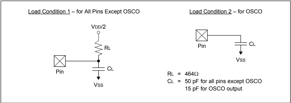
Load Condition 2 – for OSCO
RL = 464Ω
CL = 50 pF for all pins except OSCO
15 pF for OSCO output
TABLE 27-14: CAPACITIVE LOADING REQUIREMENTS ON OUTPUT PINS
| Param No. | Symbol | Characteristic | Min | Typ(1) | Max | Units | Conditions |
|---|---|---|---|---|---|---|---|
| DO50 | Cosc2 | OSCO/CLKO Pin | — | — | 15 | pF | In XT and HS modes when external clock is used to drive OSCI |
| DO56 | CIO | All I/O Pins and OSCO | — | — | 50 | pF | EC mode |
| DO58 | CB | SCLx, SDAx | — | — | 400 | pF | In I²C™ mode |
Note 1: Data in “Typ” column is at 3.3V, +25°C unless otherwise stated. Parameters are for design guidance only and are not tested.
FIGURE 27-4: EXTERNAL CLOCK TIMING
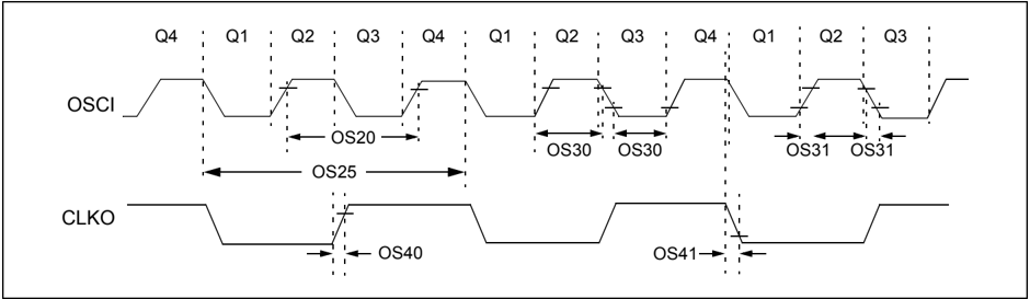
TABLE 27-15: EXTERNAL CLOCK TIMING REQUIREMENTS
AC CHARACTERISTICS
Standard Operating Conditions: 2.0 to 3.6V (unless otherwise stated)
Operating temperature
-40°C ≤ TA ≤ +85°C for Industrial
-40°C ≤ TA ≤ +125°C for Extended
| Param No. | Sym | Characteristic | Min | Typ(1) | Max | Units | Conditions |
|---|---|---|---|---|---|---|---|
| OS10 | FOSC | External CLKI Frequency (External clocks allowed only in EC mode) | DC 4 | — | 32 8 | MHz MHz | EC, -40°C ≤ TA ≤ +85°C ECPLL, -40°C ≤ TA ≤ +85°C |
| DC 4 | — | 24 6 | MHz MHz | EC, -40°C ≤ TA ≤ +125°C ECPLL, -40°C ≤ TA ≤ +125°C | |||
| Oscillator Frequency | 3 | — | 10 | MHz | XT | ||
| 3 | — | 8 | MHz | XTPLL, -40°C ≤ TA ≤ +85°C | |||
| 10 | — | 32 | MHz | HS, -40°C ≤ TA ≤ +85°C | |||
| 31 | — | 33 | kHz | SOSC | |||
| 3 | — | 6 | MHz | XTPLL, -40°C ≤ TA ≤ +125°C | |||
| 10 | — | 24 | MHz | HS, -40°C ≤ TA ≤ +125°C | |||
| OS20 | TOSC | TOSC = 1/FOSC | — | — | — | — | See Parameter OS10 for Fosc value |
| OS25 | TCY | Instruction Cycle Time(2) | 62.5 | — | DC | ns | |
| OS30 | TosL, TosH | External Clock In (OSCI) High or Low Time | 0.45 x Tosc | — | — | ns | EC |
| OS31 | TosR, TosF | External Clock In (OSCI) Rise or Fall Time | — | — | 20 | ns | EC |
| OS40 | TckR | CLKO Rise Time(3) | — | 6 | 10 | ns | |
| OS41 | TckF | CLKO Fall Time(3) | — | 6 | 10 | ns |
Note 1: Data in “Typ” column is at 3.3V, +25°C unless otherwise stated. Parameters are for design guidance only and are not tested.
2: Instruction cycle period (TCY) equals two times the input oscillator time base period. All specified values are based on characterization data for that particular oscillator type, under standard operating conditions, with the device executing code. Exceeding these specified limits may result in an unstable oscillator operation and/or higher than expected current consumption. All devices are tested to operate at “Min.” values with an external clock applied to the OSCI/CLKI pin. When an external clock input is used, the “Max.” cycle time limit is “DC” (no clock) for all devices.
3: Measurements are taken in EC mode. The CLKO signal is measured on the OSCO pin. CLKO is low for the Q1-Q2 period (1/2 TCY) and high for the Q3-Q4 period (1/2 TCY).
TABLE 27-16: PLL CLOCK TIMING SPECIFICATIONS (VDD = 2.0V TO 3.6V)
| AC CHARACTERISTICS | Standard Operating Conditions: 2.0V to 3.6V (unless otherwise stated) Operating temperature -40°C ≤ TA ≤ +85°C for Industrial -40°C ≤ TA ≤ +125°C for Extended | ||||||
|---|---|---|---|---|---|---|---|
| Param No. | Sym | Characteristic(1) | Min | Typ(2) | Max | Units | Conditions |
| OS50 | FPLLI | PLL Input Frequency Range | 3 | — | 8 | MHz | ECPLL, HSPLL, XTPLL modes, -40°C ≤ TA ≤ +85°C |
| 3 | — | 6 | MHz | ECPLL, HSPLL, XTPLL modes, -40°C ≤ TA ≤ +125°C | |||
| OS51 | Fsys | PLL Output Frequency Range | 8 | — | 32 | MHz | -40°C ≤ TA ≤ +85°C |
| 8 | — | 24 | MHz | -40°C ≤ TA ≤ +125°C | |||
| OS52 | TLOCK | PLL Start-up Time (Lock Time) | — | — | 2 | ms | |
| OS53 | DCLK | CLKO Stability (Jitter) | -2 | 1 | 2 | % | Measured over 100 ms period |
Note 1: These parameters are characterized but not tested in manufacturing.
2: Data in “Typ” column is at 3.3V, +25°C unless otherwise stated. Parameters are for design guidance only and are not tested.
TABLE 27-17: INTERNAL RC OSCILLATOR SPECIFICATIONS
| AC CHARACTERISTICS | Standard Operating Conditions: 2.0V to 3.6V (unless otherwise stated) Operating temperature -40°C ≤ TA ≤ +85°C for Industrial -40°C ≤ TA ≤ +125°C for Extended | ||||||
|---|---|---|---|---|---|---|---|
| Param No. | Sym | Characteristic | Min | Typ | Max | Units | Conditions |
| TFRC | FRC Start-up Time | — | 15 | — | µs | ||
| TLPRC | LPRC Start-up Time | — | 40 | — | µs |
TABLE 27-18: AC CHARACTERISTICS: INTERNAL RC ACCURACY
| AC CHARACTERISTICS | Standard Operating Conditions: 2.0V to 3.6V (unless otherwise stated) Operating temperature -40°C ≤ TA ≤ +85°C for Industrial -40°C ≤ TA ≤ +125°C for Extended | |||||
|---|---|---|---|---|---|---|
| Param No. | Characteristic | Min | Typ | Max | Units | Conditions |
| F20 | Internal FRC @ 8 MHz(1) | -2 | — | 2 | % | +25°C |
| -5 | — | 5 | % | -40°C ≤ TA ≤ +85°C | ||
| -7 | — | 7 | % | +125°C | ||
| F21 | LPRC @ 31 kHz(2) | -15 | — | 15 | % | +25°C |
| -15 | — | 15 | % | -40°C ≤ TA ≤ +85°C | ||
| -30 | — | 30 | % | +125°C |
Note 1: Frequency calibrated at +25°C and 3.3V. OSCTUN bits can be used to compensate for temperature drift.
2: Change of LPRC frequency as VDD changes.
FIGURE 27-5: CLKO AND I/O TIMING CHARACTERISTICS
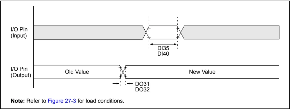
Note: Refer to Figure 27-3 for load conditions.
TABLE 27-19: CLKO AND I/O TIMING REQUIREMENTS
AC CHARACTERISTICS
Standard Operating Conditions: 2.0V to 3.6V (unless otherwise stated)
Operating temperature
-40°C ≤ TA ≤ +85°C for Industrial
-40°C ≤ TA ≤ +125°C for Extended
| Param No. | Sym | Characteristic | Min | Typ(1) | Max | Units | Conditions |
|---|---|---|---|---|---|---|---|
| DO31 | TioR | Port Output Rise Time | — | 10 | 25 | ns | |
| DO32 | TioF | Port Output Fall Time | — | 10 | 25 | ns | |
| DI35 | TINP | INTx Pin High or Low Time (output) | 20 | — | — | ns | |
| DI40 | TRBP | CNx High or Low Time (input) | 2 | — | — | TCY |
Note 1: Data in “Typ” column is at 3.3V, +25°C unless otherwise stated.
TABLE 27-20: A/D MODULE SPECIFICATIONS
AC CHARACTERISTICS
Standard Operating Conditions: 2.0V to 3.6V (unless otherwise stated)
Operating temperature
-40°C ≤ TA ≤ +85°C for Industrial
-40°C ≤ TA ≤ +125°C for Extended
| Param No. | Symbol | Characteristic | Min. | Typ | Max. | Units | Conditions |
|---|---|---|---|---|---|---|---|
| Device Supply | |||||||
| AD01 | AVDD | Module VDD Supply | Greater of: VDD – 0.3 or 2.0 | — | Lesser of: VDD + 0.3 or 3.6 | V | |
| AD02 | AVSS | Module VSS Supply | VSS – 0.3 | — | VSS + 0.3 | V | |
| Reference Inputs | |||||||
| AD05 | VREFH | Reference Voltage High | AVSS + 1.7 | — | AVDD | V | |
| AD06 | VREFL | Reference Voltage Low | AVSS | — | AVDD – 1.7 | V | |
| AD07 | VREF | Absolute Reference Voltage | AVSS – 0.3 | — | AVDD + 0.3 | V | |
| AD08 | IVREF | Reference Voltage Input Current | — | — | 1.25 | mA | Measured during conversion, 3.3V, +25°C (Note 1) |
| AD09 | ZREF | Reference Input Impedance | — | 10k | — | Ω | Measured during sampling, 3.3V, +25°C |
| Analog Input | |||||||
| AD10 | VINH-VINL | Full-Scale Input Span | VREFL | — | VREFH | V | (Note 1) |
| AD11 | VIN | Absolute Input Voltage | AVSS – 0.3 | — | AVDD + 0.3 | V | |
| AD12 | VINL | Absolute VINL Input Voltage | AVSS – 0.3 | — | AVDD/2 | V | |
| AD13 | — | Leakage Current | — | ±1 | ±610 | nA | VINL = AVSS = VREFL = 0V, AVDD = VREFH = 3V, Source Impedance = 2.5 kΩ |
| AD17 | RIN | Recommended Impedance of Analog Voltage Source | — | — | 2.5K | Ω | 10-bit |
| A/D Accuracy | |||||||
| AD20b | Nr | Resolution | — | 10 | — | bits | |
| AD21b | INL | Integral Nonlinearity | — | ±1 | <±2 | LSb | VINL = AVSS = VREFL = 0V, AVDD = VREFH = 3V |
| AD22b | DNL | Differential Nonlinearity | — | ±1 | <±1.25 | LSb | VINL = AVSS = VREFL = 0V, AVDD = VREFH = 3V |
| AD23b | GERR | Gain Error | — | ±1 | ±3 | LSb | VINL = AVSS = VREFL = 0V, AVDD = VREFH = 3V |
| AD24b | EOFF | Offset Error | — | ±1 | ±2 | LSb | VINL = AVSS = VREFL = 0V, AVDD = VREFH = 3V |
| AD25b | — | Monotonicity(2) | — | — | — | — | Guaranteed |
Note 1: Measurements are taken with external VREF+ and VREF- used as the A/D voltage reference.
2: The A/D conversion result never decreases with an increase in the input voltage and has no missing codes.
TABLE 27-21: A/D CONVERSION TIMING REQUIREMENTS(1)
AC CHARACTERISTICS
Standard Operating Conditions: 2.0V to 3.6V (unless otherwise stated)
Operating temperature
-40°C ≤ TA ≤ +85°C for Industrial
-40°C ≤ TA ≤ +125°C for Extended
| Param No. | Symbol | Characteristic | Min. | Typ | Max. | Units | Conditions |
|---|---|---|---|---|---|---|---|
| Clock Parameters | |||||||
| AD50 | TAD | A/D Clock Period | 75 | — | — | ns | TCY = 75 ns, AD1CON3 in default state |
| AD51 | tRC | A/D Internal RC Oscillator Period | — | 250 | — | ns | |
| Conversion Rate | |||||||
| AD55 | tCONV | Conversion Time | — | 12 | — | TAD | |
| AD56 | FCNV | Throughput Rate | — | — | 500 | ksps | AVDD ≥ 2.7V |
| AD57 | tSAMP | Sample Time | — | 1 | — | TAD | |
| Clock Parameters | |||||||
| AD61 | tPSS | Sample Start Delay from Setting Sample bit (SAMP) | 2 | — | 3 | TAD |
Note 1: Because the sample caps will eventually lose charge, clock rates below 10 kHz can affect linearity performance, especially at elevated temperatures.
NOTES:
DS39881E-page 250 © 2010-2013 Microchip Technology Inc.