23.0 COMPARATOR VOLTAGE REFERENCE
Note: This data sheet summarizes the features of this group of PIC24F devices. It is not intended to be a comprehensive reference source. For more information, refer to the “PIC24F Family Reference Manual”, “Comparator Voltage Reference Module” (DS39709).
23.1 Configuring the Comparator Voltage Reference
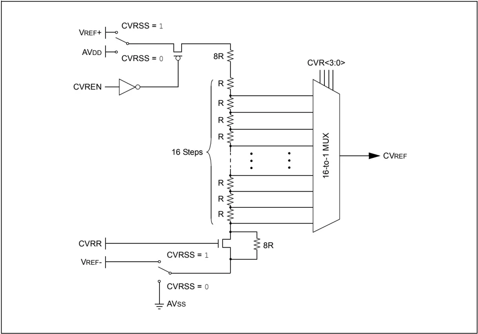
The comparator voltage reference module is controlled through the CVRCON register (Register 23-1). The comparator voltage reference provides two ranges of output voltage, each with 16 distinct levels. The range to be used is selected by the CVRR bit (CVRCON<5>). The primary difference between the ranges is the size of the steps selected by the CVREF Selection bits (CVR<3:0>), with one range offering finer resolution.
The comparator reference supply voltage can come from either VDD and VSS, or the external VREF+ and VREF-. The voltage source is selected by the CVRSS bit (CVRCON<4>).
The settling time of the comparator voltage reference must be considered when changing the CVREF output.
FIGURE 23-1: COMPARATOR VOLTAGE REFERENCE BLOCK DIAGRAM
REGISTER 23-1: CVRCON: COMPARATOR VOLTAGE REFERENCE CONTROL REGISTER
| U-0 | U-0 | U-0 | U-0 | U-0 | U-0 | U-0 | U-0 |
|---|---|---|---|---|---|---|---|
| — | — | — | — | — | — | — | — |
| bit 15 | bit 8 |
| R/W-0 | R/W-0 | R/W-0 | R/W-0 | R/W-0 | R/W-0 | R/W-0 | R/W-0 |
|---|---|---|---|---|---|---|---|
| CVREN | CVROE | CVRR | CVRSS | CVR3 | CVR2 | CVR1 | CVR0 |
| bit 7 | bit 0 |
Legend:
R = Readable bit
W = Writable bit
U = Unimplemented bit, read as ‘0’
-n = Value at POR
‘1’ = Bit is set
‘0’ = Bit is cleared
x = Bit is unknown
bit 15-8 Unimplemented: Read as ‘0’
bit 7 CVREN: Comparator Voltage Reference Enable bit
1 = CVREF circuit is powered on
0 = CVREF circuit is powered down
bit 6 CVROE: Comparator VREF Output Enable bit
1 = CVREF voltage level is output on the CVREF pin
0 = CVREF voltage level is disconnected from the CVREF pin
bit 5 CVRR: Comparator VREF Range Selection bit
1 = CVRSRC range should be 0 to 0.625 CVRSRC with CVRSRC/24 step-size
0 = CVRSRC range should be 0.25 to 0.719 CVRSRC with CVRSRC/32 step-size
bit 4 CVRSS: Comparator VREF Source Selection bit
1 = Comparator reference source, CVRSRC = VREF+ – VREF-
0 = Comparator reference source, CVRSRC = AVDD – AVSS
bit 3-0 CVR<3:0>: Comparator VREF Value Selection 0 ≤ CVR<3:0> ≤ 15 bits
When CVRR = 1:
CVREF = (CVR<3:0>/24) • (CVRSRC)
When CVRR = 0:
CVREF = 1/4 • (CVRSRC) + (CVR<3:0>/32) • (CVRSRC)
24.0 SPECIAL FEATURES
Note: This data sheet summarizes the features of this group of PIC24F devices. It is not intended to be a comprehensive reference source. For more information, refer to the following sections of the “PIC24F Family Reference Manual”:
- “Watchdog Timer (WDT)” (DS39697)
- “High-Level Device Integration” (DS39719)
- “Programming and Diagnostics” (DS39716)
PIC24FJ64GA004 family devices include several features intended to maximize application flexibility and reliability, and minimize cost through elimination of external components. These are:
- Flexible Configuration
- Watchdog Timer (WDT)
- Code Protection
- JTAG Boundary Scan Interface
- In-Circuit Serial Programming
- In-Circuit Emulation
24.1 Configuration Bits
The Configuration bits can be programmed (read as ‘0’), or left unprogrammed (read as ‘1’), to select various device configurations. These bits are mapped starting at program memory location, F80000h. A complete list of locations is shown in Table 24-1. A detailed explanation of the various bit functions is provided in Register 24-1 through Register 24-4.
Note that address, F80000h, is beyond the user program memory space. In fact, it belongs to the configuration memory space (800000h-FFFFFFh), which can only be accessed using table reads and table writes.
24.1.1 CONSIDERATIONS FOR CONFIGURING PIC24FJ64GA004 FAMILY DEVICES
In PIC24FJ64GA004 family devices, the configuration bytes are implemented as volatile memory. This means that configuration data must be programmed each time the device is powered up. Configuration data is stored in the two words at the top of the on-chip program memory space, known as the Flash Configuration Words. Their specific locations are shown in Table 24-1. These are packed representations of the actual device Configuration bits, whose actual locations are distributed among five locations in configuration space. The configuration data is automatically loaded from the Flash Configuration Words to the proper Configuration registers during device Resets.
Note: Configuration data is reloaded on all types of device Resets.
TABLE 24-1: FLASH CONFIGURATION WORD LOCATIONS FOR PIC24FJ64GA004 FAMILY DEVICES
| Device | Configuration Word Addresses | |
|---|---|---|
| 1 | 2 | |
| PIC24FJ16GA | 002BFEh | 002BFCh |
| PIC24FJ32GA | 0057FEh | 0057FCh |
| PIC24FJ48GA | 0083FEh | 0083FCh |
| PIC24FJ64GA | 00ABFEh | 00ABFCh |
When creating applications for these devices, users should always specifically allocate the location of the Flash Configuration Word for configuration data. This is to make certain that program code is not stored in this address when the code is compiled.
The Configuration bits are reloaded from the Flash Configuration Word on any device Reset.
The upper byte of both Flash Configuration Words in program memory should always be ‘1111 1111’. This makes them appear to be NOP instructions in the remote event that their locations are ever executed by accident. Since Configuration bits are not implemented in the corresponding locations, writing ‘1’s to these locations has no effect on device operation.
REGISTER 24-1: CW1: FLASH CONFIGURATION WORD 1
| U-1 | U-1 | U-1 | U-1 | U-1 | U-1 | U-1 | U-1 |
|---|---|---|---|---|---|---|---|
| — | — | — | — | — | — | — | — |
| bit 23 | bit 16 |
| r-x | R/PO-1 | R/PO-1 | R/PO-1 | R/PO-1 | r-1 | R/PO-1 | R/PO-1 |
|---|---|---|---|---|---|---|---|
| r | JTAGEN | GCP | GWRP | DEBUG | r | ICS1 | ICS0 |
| bit 15 | bit 8 |
| R/PO-1 | R/PO-1 | r | R/PO-1 | R/PO-1 | R/PO-1 | R/PO-1 | R/PO-1 |
|---|---|---|---|---|---|---|---|
| FWD TEN | WINDIS | r | FWPSA | WDTPS3 | WDTPS2 | WDTPS1 | WDTPS0 |
| bit 7 | bit 0 |
Legend:
r = Reserved bit
R = Readable bit
PO = Program Once bit
U = Unimplemented bit, read as ‘0’
-n = Value when device is unprogrammed
‘1’ = Bit is set
‘0’ = Bit is cleared
bit 23-16 Unimplemented: Read as ‘1’
bit 15 Reserved: The value is unknown; program as ‘0’
bit 14 JTAGEN: JTAG Port Enable bit
1 = JTAG port is enabled
0 = JTAG port is disabled
bit 13 GCP: General Segment Program Memory Code Protection bit
1 = Code protection is disabled
0 = Code protection is enabled for the entire program memory space
bit 12 GWRP: General Segment Code Flash Write Protection bit
1 = Writes to program memory are allowed
0 = Writes to program memory are disabled
bit 11 DEBUG: Background Debugger Enable bit
1 = Device resets into Operational mode
0 = Device resets into Debug mode
bit 10 Reserved: Always maintain as ‘1’
bit 9-8 ICS<1:0>: Emulator Pin Placement Select bits
11 = Emulator EMUC1/EMUD1 pins are shared with PGC1/PGD1
10 = Emulator EMUC2/EMUD2 pins are shared with PGC2/PGD2
01 = Emulator EMUC3/EMUD3 pins are shared with PGC3/PGD3
00 = Reserved; do not use
bit 7 FWD TEN: Watchdog Timer Enable bit
1 = Watchdog Timer is enabled
0 = Watchdog Timer is disabled
bit 6 WINDIS: Windowed Watchdog Timer Disable bit
1 = Standard Watchdog Timer is enabled
0 = Windowed Watchdog Timer is enabled; FWD TEN must be ‘1’
bit 5 Reserved
bit 4 FWPSA: WDT Prescaler Ratio Select bit
1 = Prescaler ratio of 1:128
0 = Prescaler ratio of 1:32
REGISTER 24-1: CW1: FLASH CONFIGURATION WORD 1 (CONTINUED)
bit 3-0 WDTPS<3:0>: Watchdog Timer Postscaler Select bits
1111 = 1:32,768
1110 = 1:16,384
1101 = 1:8,192
1100 = 1:4,096
1011 = 1:2,048
1010 = 1:1,024
1001 = 1:512
1000 = 1:256
0111 = 1:128
0110 = 1:64
0101 = 1:32
0100 = 1:16
0011 = 1:8
0010 = 1:4
0001 = 1:2
0000 = 1:1
REGISTER 24-2: CW2: FLASH CONFIGURATION WORD 2
| U-1 | U-1 | U-1 | U-1 | U-1 | U-1 | U-1 | U-1 |
|---|---|---|---|---|---|---|---|
| — | — | — | — | — | — | — | — |
| bit 23 | bit 16 |
| R/PO-1 | R/PO-1 | R/PO-1 | R/PO-1 | R/PO-1 | R/PO-1 | R/PO-1 | R/PO-1 |
|---|---|---|---|---|---|---|---|
| IESO | WUTSEL1⁽¹⁾ | WUTSEL0⁽¹⁾ | SOSCSEL1⁽¹⁾ | SOSCSEL0⁽¹⁾ | FNOSC2 | FNOSC1 | FNOSC0 |
| bit 15 | bit 8 |
| R/PO-1 | R/PO-1 | R/PO-1 | R/PO-1 | r | R/PO-1 | R/PO-1 | R/PO-1 |
|---|---|---|---|---|---|---|---|
| FCKSM1 | FCKSM0 | OSCIOFCN | IOL1WAY | r | I2C1SEL | POSCMD1 | POSCMD0 |
| bit 7 | bit 0 |
Legend:
r = Reserved bit
R = Readable bit
PO = Program Once bit
U = Unimplemented bit, read as ‘0’
-n = Value when device is unprogrammed
‘1’ = Bit is set
‘0’ = Bit is cleared
bit 23-16 Unimplemented: Read as ‘1’
bit 15 IESO: Internal External Switchover bit
1 = IESO mode (Two-Speed Start-up) is enabled
0 = IESO mode (Two-Speed Start-up) is disabled
bit 14-13 WUTSEL<1:0>: Voltage Regulator Standby Mode Wake-up Time Select bits⁽¹⁾
11 = Default regulator start-up time is used
01 = Fast regulator start-up time is used
x0 = Reserved; do not use
bit 12-11 SOSCSEL<1:0>: Secondary Oscillator Power Mode Select bits⁽¹⁾
11 = Default (High Drive Strength) mode
01 = Low-Power (Low Drive Strength) mode
x0 = Reserved; do not use
bit 10-8 FNOSC<2:0>: Initial Oscillator Select bits
111 = Fast RC Oscillator with Postscaler (FRC DIV)
110 = Reserved
101 = Low-Power RC Oscillator (LPRC)
100 = Secondary Oscillator (SOSC)
011 = Primary Oscillator with PLL module (XTPLL, HSPLL, ECPLL)
010 = Primary Oscillator (XT, HS, EC)
001 = Fast RC Oscillator with Postscaler and PLL module (FRCPLL)
000 = Fast RC Oscillator (FRC)
bit 7-6 FCKSM<1:0>: Clock Switching and Fail-Safe Clock Monitor Configuration bits
1x = Clock switching and Fail-Safe Clock Monitor are disabled
01 = Clock switching is enabled, Fail-Safe Clock Monitor is disabled
00 = Clock switching is enabled, Fail-Safe Clock Monitor is enabled
bit 5 OSCIOFCN: OSCO Pin Configuration bit
If POSCMD<1:0> = 11 or 00:
1 = OSCO/CLKO/RA3 functions as CLKO (Fosc/2)
0 = OSCO/CLKO/RA3 functions as port I/O (RA3)
If POSCMD<1:0> = 10 or 01:
OSCI OFCN has no effect on OSCO/CLKO/RA3.
Note 1: These bits are implemented only in devices with a major silicon revision level of B or later (DEVREV register value is 3042h or greater). Refer to Section 28.0 “Packaging Information” in the device data sheet for the location and interpretation of product date codes.
REGISTER 24-2: CW2: FLASH CONFIGURATION WORD 2 (CONTINUED)
bit 4
IOL1WAY: IOLOCK One-Way Set Enable bit
1 = The IOLOCK (OSCCON<6>) bit can be set once, provided the unlock sequence has been completed. Once set, the Peripheral Pin Select registers cannot be written to a second time.
0 = The IOLOCK (OSCCON<6>) bit can be set and cleared as needed, provided the unlock sequence has been completed
bit 3
Reserved
bit 2
I2C1SEL: I2C1 Pin Select bit
1 = Use default SCL1/SDA1 pins
0 = Use alternate SCL1/SDA1 pins
bit 1-0
POSCMD<1:0>: Primary Oscillator Configuration bits
11 = Primary oscillator is disabled
10 = HS Oscillator mode is selected
01 = XT Oscillator mode is selected
00 = EC Oscillator mode is selected
Note 1: These bits are implemented only in devices with a major silicon revision level of B or later (DEVREV register value is 3042h or greater). Refer to Section 28.0 “Packaging Information” in the device data sheet for the location and interpretation of product date codes.
REGISTER 24-3: DEVID: DEVICE ID REGISTER
| U | U | U | U | U | U | U | U |
|---|---|---|---|---|---|---|---|
| — | — | — | — | — | — | — | — |
| bit 23 | bit 16 |
| U | U | R | R | R | R | R | R |
|---|---|---|---|---|---|---|---|
| — | — | FAMID7 | FAMID6 | FAMID5 | FAMID4 | FAMID3 | FAMID2 |
| bit 15 | bit 8 |
| R | R | R | R | R | R | R | R |
|---|---|---|---|---|---|---|---|
| FAMID1 | FAMID0 | DEV5 | DEV4 | DEV3 | DEV2 | DEV1 | DEV0 |
| bit 7 | bit 0 |
Legend: R = Read-only bit
U = Unimplemented bit
bit 23-14
Unimplemented: Read as ‘1’
bit 13-6
FAMID<7:0>: Device Family Identifier bits
00010001 = PIC24FJ64GA004 family
bit 5-0
DEV<5:0>: Individual Device Identifier bits
000100 = PIC24FJ16GA002
000101 = PIC24FJ32GA002
000110 = PIC24FJ48GA002
000111 = PIC24FJ64GA002
001100 = PIC24FJ16GA004
001101 = PIC24FJ32GA004
001110 = PIC24FJ48GA004
001111 = PIC24FJ64GA004

REGISTER 24-4: DEVREV: DEVICE REVISION REGISTER
Legend: R = Read-only bit U = Unimplemented bit
bit 23-9 Unimplemented: Read as ‘0’ bit 8-6 MAJRV<2:0>: Major Revision Identifier bits bit 5-3 Unimplemented: Read as ‘0’ bit 2-0 DOT<2:0>: Minor Revision Identifier bits
DS39881E-page 214 © 2010-2013 Microchip Technology Inc.
24.2 On-Chip Voltage Regulator
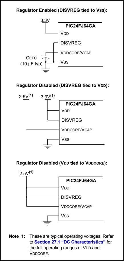
All of the PIC24FJ64GA004 family devices power their core digital logic at a nominal 2.5V. This may create an issue for designs that are required to operate at a higher typical voltage, such as 3.3V. To simplify system design, all devices in the PIC24FJ64GA004 family incorporate an on-chip regulator that allows the device to run its core logic from VDD.
The regulator is controlled by the DISVREG pin. Tying VSS to the pin enables the regulator, which in turn, provides power to the core from the other VDD pins. When the regulator is enabled, a low-ESR capacitor (such as ceramic) must be connected to the VDDCORE/VCAP pin (Figure 24-1). This helps to maintain the stability of the regulator. The recommended value for the filter capacitor is provided in Section 27.1 “DC Characteristics”.
If DISVREG is tied to VDD, the regulator is disabled. In this case, separate power for the core logic at a nominal 2.5V must be supplied to the device on the VDDCORE/VCAP pin to run the I/O pins at higher voltage levels, typically 3.3V. Alternatively, the VDDCORE/VCAP and VDD pins can be tied together to operate at a lower nominal voltage. Refer to Figure 24-1 for possible configurations.
24.2.1 VOLTAGE REGULATOR TRACKING MODE AND LOW-VOLTAGE DETECTION
When it is enabled, the on-chip regulator provides a constant voltage of 2.5V nominal to the digital core logic.
The regulator can provide this level from a VDD of about 2.5V, all the way up to the device’s VDDMAX. It does not have the capability to boost VDD levels below 2.5V. In order to prevent “brown out” conditions, when the voltage drops too low for the regulator, the regulator enters Tracking mode. In Tracking mode, the regulator output follows VDD, with a typical voltage drop of 100 mV.
When the device enters Tracking mode, it is no longer possible to operate at full speed. To provide information about when the device enters Tracking mode, the on-chip regulator includes a simple, Low-Voltage Detect (LVD) circuit. When VDD drops below full-speed operating voltage, the circuit sets the Low-Voltage Detect Interrupt Flag, LVDIF (IFS4<8>). This can be used to generate an interrupt and put the application into a low-power operational mode or trigger an orderly shutdown.
Low-Voltage Detection is only available when the regulator is enabled.
FIGURE 24-1: CONNECTIONS FOR THE ON-CHIP REGULATOR
Note 1: These are typical operating voltages. Refer to Section 27.1 “DC Characteristics” for the full operating ranges of VDD and VDDCORE.
24.2.2 ON-CHIP REGULATOR AND BOR
When the on-chip regulator is enabled, PIC24FJ64GA004 family devices also have a simple brown-out capability. If the voltage supplied to the regulator is inadequate to maintain the tracking level, the regulator Reset circuitry will generate a Brown-out Reset. This event is captured by the BOR flag bit (RCON<1>). The brown-out voltage levels are specified in Section 27.1 “DC Characteristics”.
24.2.3 ON-CHIP REGULATOR AND POR
When the voltage regulator is enabled, it takes approximately 10 µs for it to generate output. During this time, designated as TVREG, code execution is disabled. TVREG is applied every time the device resumes operation after any power-down, including Sleep mode. TVREG is determined by the setting of the PMSLP bit (RCON<8>) and the WUTSELx Configuration bits (CW2<14:13>). For more information on TVREG, see Section 27.0 “Electrical Characteristics”.
If the regulator is disabled, a separate Power-up Timer (PWRT) is automatically enabled. The PWRT adds a fixed delay of 64 ms nominal delay at device start-up (POR or BOR only). When waking up from Sleep with the regulator disabled, TVREG is used to determine the wake-up time. To decrease the device wake-up time when operating with the regulator disabled, the PMSLP bit can be set.
24.2.4 POWER-UP REQUIREMENTS
The on-chip regulator is designed to meet the power-up requirements for the device. If the application does not use the regulator, then strict power-up conditions must be adhered to. While powering up, VDDCORE must never exceed VDD by 0.3 volts.
Note: For more information, see Section 27.0 “Electrical Characteristics”.
24.2.5 VOLTAGE REGULATOR STANDBY MODE
When enabled, the on-chip regulator always consumes a small incremental amount of current over IDD/IPD, including when the device is in Sleep mode, even though the core digital logic does not require power. To provide additional savings in applications where power resources are critical, the regulator automatically places itself into Standby mode whenever the device goes into Sleep mode. This feature is controlled by the PMSLP bit (RCON<8>). By default, this bit is cleared, which enables Standby mode.
For select PIC24FJ64GA004 family devices, the time required for regulator wake-up from Standby mode is controlled by the WUTSEL<1:0> Configuration bits (CW2<14:13>). The default wake-up time for all devices is 190 µs. Where the WUTSELx Configuration bits are implemented, a fast wake-up option is also available. When WUTSEL<1:0> = 01, the regulator wake-up time is 25 µs.
Note: This feature is implemented only on PIC24FJ64GA004 family devices with a major silicon revision level of B or later (DEVREV register value is 3042h or greater).
When the regulator’s Standby mode is turned off (PMSLP = 1), Flash program memory stays powered in Sleep mode and the device can wake-up in less than 10 µs. When PMSLP is set, the power consumption while in Sleep mode will be approximately 40 µA higher than power consumption when the regulator is allowed to enter Standby mode.
24.3 Watchdog Timer (WDT)
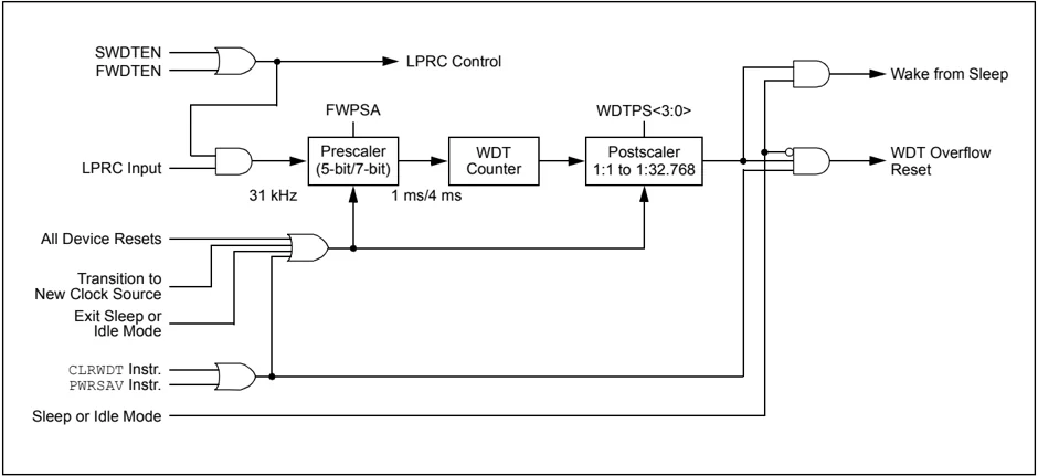
For PIC24FJ64GA004 family devices, the WDT is driven by the LPRC oscillator. When the WDT is enabled, the clock source is also enabled.
The nominal WDT clock source from LPRC is 31 kHz. This feeds a prescaler that can be configured for either 5-bit (divide-by-32) or 7-bit (divide-by-128) operation. The prescaler is set by the FWPSA Configuration bit. With a 31 kHz input, the prescaler yields a nominal WDT Time-out period (TWDT) of 1 ms in 5-bit mode or 4 ms in 7-bit mode.
A variable postscaler divides down the WDT prescaler output and allows for a wide range of time-out periods. The postscaler is controlled by the WDTPS<3:0> Configuration bits (CW1<3:0>), which allow the selection of a total of 16 settings, from 1:1 to 1:32,768. Using the prescaler and postscaler, time-out periods, ranges from 1 ms to 131 seconds can be achieved.
The WDT, prescaler and postscaler are reset:
- On any device Reset
- On the completion of a clock switch, whether invoked by software (i.e., setting the OSWEN bit after changing the NOSCx bits) or by hardware (i.e., Fail-Safe Clock Monitor)
- When a PWRSAV instruction is executed (i.e., Sleep or Idle mode is entered)
- When the device exits Sleep or Idle mode to resume normal operation
- By a CLRWDT instruction during normal execution
If the WDT is enabled, it will continue to run during Sleep or Idle modes. When the WDT time-out occurs, the device will wake the device and code execution will continue from where the PWRSAV instruction was executed. The corresponding SLEEP or IDLE bits (RCON<3:2>) will need to be cleared in software after the device wakes up.
The WDT Flag bit, WDTO (RCON<4>), is not automatically cleared following a WDT time-out. To detect subsequent WDT events, the flag must be cleared in software.
Note: The CLRWDT and PWRSAV instructions clear the prescaler and postscaler counts when executed.
24.3.1 WINDOWED OPERATION
The Watchdog Timer has an optional Fixed Window mode of operation. In this Windowed mode, CLRWDT instructions can only reset the WDT during the last 1/4 of the programmed WDT period. A CLRWDT instruction executed before that window causes a WDT Reset, similar to a WDT time-out.
Windowed WDT mode is enabled by programming the WINDIS Configuration bit (CW1<6>) to ‘0’.
24.3.2 CONTROL REGISTER
The WDT is enabled or disabled by the FWDTEN Configuration bit. When the FWDTEN Configuration bit is set, the WDT is always enabled.
The WDT can be optionally controlled in software when the FWDTEN Configuration bit has been programmed to ‘0’. The WDT is enabled in software by setting the SWDTEN control bit (RCON<5>). The SWDTEN control bit is cleared on any device Reset. The software WDT option allows the user to enable the WDT for critical code segments and disable the WDT during non-critical segments for maximum power savings.
FIGURE 24-2: WDT BLOCK DIAGRAM
24.4 JTAG Interface
PIC24FJ64GA004 family devices implement a JTAG interface, which supports boundary scan device testing.
24.5 Program Verification and Code Protection
For all devices in the PIC24FJ64GA004 family, the on-chip program memory space is treated as a single block. Code protection for this block is controlled by one Configuration bit, GCP. This bit inhibits external reads and writes to the program memory space. It has no direct effect in normal execution mode.
Write protection is controlled by the GWRP bit in Configuration Word 1. When GWRP is programmed to '0', internal write and erase operations to program memory are blocked.
24.5.1 CONFIGURATION REGISTER PROTECTION
The Configuration registers are protected against inadvertent or unwanted changes, or reads in two ways. The primary protection method is the same as that of the RP registers – shadow registers contain a complimentary value which is constantly compared with the actual value.
To safeguard against unpredictable events, Configuration bit changes, resulting from individual cell level disruptions (such as ESD events), will cause a parity error and trigger a device Reset.
The data for the Configuration registers is derived from the Flash Configuration Words in program memory. When the GCP bit is set, the source data for device configuration is also protected as a consequence.
24.6 In-Circuit Serial Programming
PIC24FJ64GA004 family microcontrollers can be serially programmed while in the end application circuit. This is simply done with two lines for clock (PGCx) and data (PGDx), and three other lines for power, ground and the programming voltage. This allows customers to manufacture boards with unprogrammed devices and then program the microcontroller just before shipping the product. This also allows the most recent firmware or a custom firmware to be programmed.
24.7 In-Circuit Debugger
When MPLAB® ICD 2 is selected as a debugger, the in-circuit debugging functionality is enabled. This function allows simple debugging functions when used with MPLAB IDE. Debugging functionality is controlled through the EMUCx (Emulation/Debug Clock) and EMUDx (Emulation/Debug Data) pins.
To use the in-circuit debugger function of the device, the design must implement ICSP connections to MCLR, VDD, VSS, PGCx, PGDx and the EMUDx/EMUCx pin pair. In addition, when the feature is enabled, some of the resources are not available for general use. These resources include the first 80 bytes of data RAM and two I/O pins.
25.0 DEVELOPMENT SUPPORT
The PIC® microcontrollers (MCU) and dsPIC® digital signal controllers (DSC) are supported with a full range of software and hardware development tools:
- Integrated Development Environment
- MPLAB® X IDE Software
- Compilers/Assemblers/Linkers
- MPLAB XC Compiler
- MPASM™ Assembler
- MPLINK™ Object Linker/ MPLIB™ Object Librarian
- MPLAB Assembler/Linker/Librarian for Various Device Families
- Simulators
- MPLAB X SIM Software Simulator
- Emulators
- MPLAB REAL ICE™ In-Circuit Emulator
- In-Circuit Debuggers/Programmers
- MPLAB ICD 3
- PICkit™ 3
- Device Programmers
- MPLAB PM3 Device Programmer
- Low-Cost Demonstration/Development Boards, Evaluation Kits and Starter Kits
- Third-party development tools
25.1 MPLAB X Integrated Development Environment Software
The MPLAB X IDE is a single, unified graphical user interface for Microchip and third-party software, and hardware development tool that runs on Windows®, Linux and Mac OS® X. Based on the NetBeans IDE, MPLAB X IDE is an entirely new IDE with a host of free software components and plug-ins for high-performance application development and debugging. Moving between tools and upgrading from software simulators to hardware debugging and programming tools is simple with the seamless user interface.
With complete project management, visual call graphs, a configurable watch window and a feature-rich editor that includes code completion and context menus, MPLAB X IDE is flexible and friendly enough for new users. With the ability to support multiple tools on multiple projects with simultaneous debugging, MPLAB X IDE is also suitable for the needs of experienced users.
Feature-Rich Editor:
- Color syntax highlighting
- Smart code completion makes suggestions and provides hints as you type
- Automatic code formatting based on user-defined rules
- Live parsing
User-Friendly, Customizable Interface:
- Fully customizable interface: toolbars, toolbar buttons, windows, window placement, etc.
- Call graph window
Project-Based Workspaces:
- Multiple projects
- Multiple tools
- Multiple configurations
- Simultaneous debugging sessions
File History and Bug Tracking:
- Local file history feature
- Built-in support for Bugzilla issue tracker
25.2 MPLAB XC Compilers
The MPLAB XC Compilers are complete ANSI C compilers for all of Microchip’s 8, 16, and 32-bit MCU and DSC devices. These compilers provide powerful integration capabilities, superior code optimization and ease of use. MPLAB XC Compilers run on Windows, Linux or MAC OS X.
For easy source level debugging, the compilers provide debug information that is optimized to the MPLAB X IDE.
The free MPLAB XC Compiler editions support all devices and commands, with no time or memory restrictions, and offer sufficient code optimization for most applications.
MPLAB XC Compilers include an assembler, linker and utilities. The assembler generates relocatable object files that can then be archived or linked with other relocatable object files and archives to create an executable file. MPLAB XC Compiler uses the assembler to produce its object file. Notable features of the assembler include:
- Support for the entire device instruction set
- Support for fixed-point and floating-point data
- Command-line interface
- Rich directive set
- Flexible macro language
- MPLAB X IDE compatibility
25.3 MPASM Assembler
The MPASM Assembler is a full-featured, universal macro assembler for PIC10/12/16/18 MCUs.
The MPASM Assembler generates relocatable object files for the MPLINK Object Linker, Intel® standard HEX files, MAP files to detail memory usage and symbol reference, absolute LST files that contain source lines and generated machine code, and COFF files for debugging.
The MPASM Assembler features include:
- Integration into MPLAB X IDE projects
- User-defined macros to streamline assembly code
- Conditional assembly for multipurpose source files
- Directives that allow complete control over the assembly process
25.4 MPLINK Object Linker/MPLIB Object Librarian
The MPLINK Object Linker combines relocatable objects created by the MPASM Assembler. It can link relocatable objects from precompiled libraries, using directives from a linker script.
The MPLIB Object Librarian manages the creation and modification of library files of precompiled code. When a routine from a library is called from a source file, only the modules that contain that routine will be linked in with the application. This allows large libraries to be used efficiently in many different applications.
The object linker/library features include:
- Efficient linking of single libraries instead of many smaller files
- Enhanced code maintainability by grouping related modules together
- Flexible creation of libraries with easy module listing, replacement, deletion and extraction
25.5 MPLAB Assembler, Linker and Librarian for Various Device Families
MPLAB Assembler produces relocatable machine code from symbolic assembly language for PIC24, PIC32 and dsPIC DSC devices. MPLAB XC Compiler uses the assembler to produce its object file. The assembler generates relocatable object files that can then be archived or linked with other relocatable object files and archives to create an executable file. Notable features of the assembler include:
- Support for the entire device instruction set
- Support for fixed-point and floating-point data
- Command-line interface
- Rich directive set
- Flexible macro language
- MPLAB X IDE compatibility
DS39881E-page 220 © 2010-2013 Microchip Technology Inc.
25.6 MPLAB X SIM Software Simulator
The MPLAB X SIM Software Simulator allows code development in a PC-hosted environment by simulating the PIC MCUs and dsPIC DSCs on an instruction level. On any given instruction, the data areas can be examined or modified and stimuli can be applied from a comprehensive stimulus controller. Registers can be logged to files for further run-time analysis. The trace buffer and logic analyzer display extend the power of the simulator to record and track program execution, actions on I/O, most peripherals and internal registers.
The MPLAB X SIM Software Simulator fully supports symbolic debugging using the MPLAB XC Compilers, and the MPASM and MPLAB Assemblers. The software simulator offers the flexibility to develop and debug code outside of the hardware laboratory environment, making it an excellent, economical software development tool.
25.7 MPLAB REAL ICE In-Circuit Emulator System
The MPLAB REAL ICE In-Circuit Emulator System is Microchip’s next generation high-speed emulator for Microchip Flash DSC and MCU devices. It debugs and programs all 8, 16 and 32-bit MCU, and DSC devices with the easy-to-use, powerful graphical user interface of the MPLAB X IDE.
The emulator is connected to the design engineer’s PC using a high-speed USB 2.0 interface and is connected to the target with either a connector compatible with in-circuit debugger systems (RJ-11) or with the new high-speed, noise tolerant, Low-Voltage Differential Signal (LVDS) interconnection (CAT5).
The emulator is field upgradable through future firmware downloads in MPLAB X IDE. MPLAB REAL ICE offers significant advantages over competitive emulators including full-speed emulation, run-time variable watches, trace analysis, complex breakpoints, logic probes, a ruggedized probe interface and long (up to three meters) interconnection cables.
25.8 MPLAB ICD 3 In-Circuit Debugger System
The MPLAB ICD 3 In-Circuit Debugger System is Microchip’s most cost-effective, high-speed hardware debugger/programmer for Microchip Flash DSC and MCU devices. It debugs and programs PIC Flash microcontrollers and dsPIC DSCs with the powerful, yet easy-to-use graphical user interface of the MPLAB IDE.
The MPLAB ICD 3 In-Circuit Debugger probe is connected to the design engineer’s PC using a high-speed USB 2.0 interface and is connected to the target with a connector compatible with the MPLAB ICD 2 or MPLAB REAL ICE systems (RJ-11). MPLAB ICD 3 supports all MPLAB ICD 2 headers.
25.9 PICkit 3 In-Circuit Debugger/ Programmer
The MPLAB PICkit 3 allows debugging and programming of PIC and dsPIC Flash microcontrollers at a most affordable price point using the powerful graphical user interface of the MPLAB IDE. The MPLAB PICkit 3 is connected to the design engineer’s PC using a full-speed USB interface and can be connected to the target via a Microchip debug (RJ-11) connector (compatible with MPLAB ICD 3 and MPLAB REAL ICE). The connector uses two device I/O pins and the Reset line to implement in-circuit debugging and In-Circuit Serial Programming™ (ICSP™).
25.10 MPLAB PM3 Device Programmer
The MPLAB PM3 Device Programmer is a universal, CE compliant device programmer with programmable voltage verification at VDDMIN and VDDMAX for maximum reliability. It features a large LCD display (128 x 64) for menus and error messages, and a modular, detachable socket assembly to support various package types. The ICSP cable assembly is included as a standard item. In Stand-Alone mode, the MPLAB PM3 Device Programmer can read, verify and program PIC devices without a PC connection. It can also set code protection in this mode. The MPLAB PM3 connects to the host PC via an RS-232 or USB cable. The MPLAB PM3 has high-speed communications and optimized algorithms for quick programming of large memory devices, and incorporates an MMC card for file storage and data applications.
25.11 Demonstration/Development Boards, Evaluation Kits, and Starter Kits
A wide variety of demonstration, development and evaluation boards for various PIC MCUs and dsPIC DSCs allows quick application development on fully functional systems. Most boards include prototyping areas for adding custom circuitry and provide application firmware and source code for examination and modification.
The boards support a variety of features, including LEDs, temperature sensors, switches, speakers, RS-232 interfaces, LCD displays, potentiometers and additional EEPROM memory.
The demonstration and development boards can be used in teaching environments, for prototyping custom circuits and for learning about various microcontroller applications.
In addition to the PICDEM™ and dsPICDEM™ demonstration/development board series of circuits, Microchip has a line of evaluation kits and demonstration software for analog filter design, KEELOQ® security ICs, CAN, IrDA®, PowerSmart battery management, SEEVAL® evaluation system, Sigma-Delta ADC, flow rate sensing, plus many more.
Also available are starter kits that contain everything needed to experience the specified device. This usually includes a single application and debug capability, all on one board.
Check the Microchip web page (www.microchip.com) for the complete list of demonstration, development and evaluation kits.
25.12 Third-Party Development Tools
Microchip also offers a great collection of tools from third-party vendors. These tools are carefully selected to offer good value and unique functionality.
• Device Programmers and Gang Programmers from companies, such as SoftLog and CCS • Software Tools from companies, such as Gimpel and Trace Systems • Protocol Analyzers from companies, such as Saleae and Total Phase • Demonstration Boards from companies, such as MikroElektronika, Digilent® and Olimex • Embedded Ethernet Solutions from companies, such as EZ Web Lynx, WIZnet and IPLogika®
DS39881E-page 222 © 2010-2013 Microchip Technology Inc.