18.0 PARALLEL MASTER PORT (PMP)
Note: This data sheet summarizes the features of this group of PIC24F devices. It is not intended to be a comprehensive reference source. For more information, refer to the “PIC24F Family Reference Manual”, “Parallel Master Port (PMP)” (DS39713).
The Parallel Master Port (PMP) module is a parallel 8-bit I/O module, specifically designed to communicate with a wide variety of parallel devices, such as communication peripherals, LCDs, external memory devices and microcontrollers. Because the interface to parallel peripherals varies significantly, the PMP is highly configurable.
Note: A number of the pins for the PMP are not present on PIC24FJ64GA004 devices. Refer to the specific device’s pinout to determine which pins are available.
Key features of the PMP module include:
- Up to 16 Programmable Address Lines
- One Chip Select Line
- Programmable Strobe Options:
- Individual Read and Write Strobes or;
- Read/Write Strobe with Enable Strobe
- Address Auto-Increment/Auto-Decrement
- Programmable Address/Data Multiplexing
- Programmable Polarity on Control Signals
- Legacy Parallel Slave Port Support
- Enhanced Parallel Slave Support:
- Address Support
- 4-Byte Deep Auto-Incrementing Buffer
- Programmable Wait States
- Selectable Input Voltage Levels
FIGURE 18-1: PARALLEL MASTER PORT (PMP) MODULE OVERVIEW
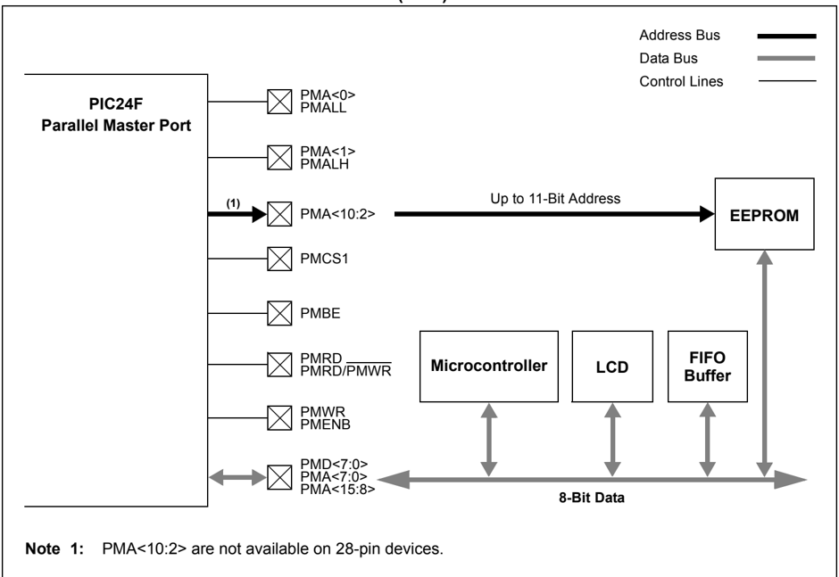
Note 1: PMA<10:2> are not available on 28-pin devices.
REGISTER 18-1: PMCON: PARALLEL PORT CONTROL REGISTER
| R/W-0 | U-0 | R/W-0 | R/W-0 | R/W-0 | R/W-0 | R/W-0 | R/W-0 |
|---|---|---|---|---|---|---|---|
| PMPEN | — | PSIDL | ADRMUX1⁽¹⁾ | ADRMUX0⁽¹⁾ | PTBEEN | PTWREN | PTRDEN |
| bit 15 | bit 8 |
| R/W-0 | R/W-0 | R/W-0⁽²⁾ | U-0 | R/W-0⁽²⁾ | R/W-0 | R/W-0 | R/W-0 |
|---|---|---|---|---|---|---|---|
| CSF1 | CSF0 | ALP | — | CS1P | BEP | WRSP | RDSP |
| bit 7 | bit 0 |
Legend:
R = Readable bit
W = Writable bit
U = Unimplemented bit, read as ‘0’
-n = Value at POR
‘1’ = Bit is set
‘0’ = Bit is cleared
x = Bit is unknown
bit 15
PMPEN: PMP Enable bit
1 = PMP is enabled
0 = PMP is disabled, no off-chip access is performed
bit 14
Unimplemented: Read as ‘0’
bit 13
PSIDL: PMP Stop in Idle Mode bit
1 = Discontinues module operation when device enters Idle mode
0 = Continues module operation in Idle mode
bit 12-11
ADRMUX<1:0>: Address/Data Multiplexing Selection bits⁽¹⁾
11 = Reserved
10 = All 16 bits of address are multiplexed on the PMD<7:0> pins
01 = Lower 8 bits of address are multiplexed on the PMD<7:0> pins, upper 3 bits are multiplexed on PMA<10:8>
00 = Address and data appear on separate pins
bit 10
PTBEEN: PMP Byte Enable Port Enable bit (16-Bit Master mode)
1 = PMBE port is enabled
0 = PMBE port is disabled
bit 9
PTWREN: PMP Write Enable Strobe Port Enable bit
1 = PMWR/PMENB port is enabled
0 = PMWR/PMENB port is disabled
bit 8
PTRDEN: PMP Read/Write Strobe Port Enable bit
1 = PMRD/PMWR port is enabled
0 = PMRD/PMWR port is disabled
bit 7-6
CSF<1:0>: Chip Select Function bits
11 = Reserved
10 = PMCS1 functions as chip set
01 = Reserved
00 = Reserved
bit 5
ALP: Address Latch Polarity bit⁽²⁾
1 = Active-high (PMALL and PMALH)
0 = Active-low (PMALL and PMALH)
bit 4
Unimplemented: Read as ‘0’
bit 3
CS1P: Chip Select 1 Polarity bit⁽²⁾
1 = Active-high (PMCS1/PMCS1)
0 = Active-low (PMCS1/PMCS1)
Note 1: PMA<10:2> bits are not available on 28-pin devices.
2: These bits have no effect when their corresponding pins are used as address lines.
REGISTER 18-1: PMCON: PARALLEL PORT CONTROL REGISTER (CONTINUED)
bit 2 BEP: Byte Enable Polarity bit 1 = Byte enable is active-high (PMBE) 0 = Byte enable is active-low (PMBE)
bit 1 WRSP: Write Strobe Polarity bit For Slave Modes and Master Mode 2 (PMMODE<9:8> = 00, 01, 10): 1 = Write strobe is active-high (PMWR) 0 = Write strobe is active-low (PMWR) For Master Mode 1 (PMMODE<9:8> = 11): 1 = Enable strobe is active-high (PMENB) 0 = Enable strobe is active-low (PMENB)
bit 0 RDSP: Read Strobe Polarity bit For Slave Modes and Master Mode 2 (PMMODE<9:8> = 00, 01, 10): 1 = Read strobe is active-high (PMRD) 0 = Read strobe is active-low (PMRD) For Master Mode 1 (PMMODE<9:8> = 11): 1 = Read/write strobe is active-high (PMRD/PMWR) 0 = Read/write strobe is active-low (PMRD/PMWR)
Note 1: PMA<10:2> bits are not available on 28-pin devices. 2: These bits have no effect when their corresponding pins are used as address lines.
REGISTER 18-2: PMMODE: PARALLEL PORT MODE REGISTER
| R-0 | R/W-0 | R/W-0 | R/W-0 | R/W-0 | R/W-0 | R/W-0 | R/W-0 |
|---|---|---|---|---|---|---|---|
| BUSY | IRQM1 | IRQM0 | INCM1 | INCM0 | MODE16 | MODE1 | MODE0 |
| bit 15 | bit 8 |
| R/W-0 | R/W-0 | R/W-0 | R/W-0 | R/W-0 | R/W-0 | R/W-0 | R/W-0 |
|---|---|---|---|---|---|---|---|
| WAITB1⁽¹⁾ | WAITB0⁽¹⁾ | WAITM3 | WAITM2 | WAITM1 | WAITM0 | WAITE1⁽¹⁾ | WAITE0⁽¹⁾ |
| bit 7 | bit 0 |
Legend:
R = Readable bit
W = Writable bit
U = Unimplemented bit, read as ‘0’
-n = Value at POR
‘1’ = Bit is set
‘0’ = Bit is cleared
x = Bit is unknown
bit 15
BUSY: Busy bit (Master mode only)
1 = Port is busy (not useful when the processor stall is active)
0 = Port is not busy
bit 14-13
IRQM<1:0>: Interrupt Request Mode bits
11 = Interrupt is generated when Read Buffer 3 is read or Write Buffer 3 is written (Buffered PSP mode)
or on a read or write operation when PMA<1:0> = 11 (Addressable PSP mode only)
10 = No interrupt is generated, processor stall is activated
01 = Interrupt is generated at the end of the read/write cycle
00 = No interrupt is generated
bit 12-11
INCM<1:0>: Increment Mode bits
11 = PSP read and write buffers auto-increment (Legacy PSP mode only)
10 = Decrements ADDR<10:0> by 1 every read/write cycle
01 = Increments ADDR<10:0> by 1 every read/write cycle
00 = No increment or decrement of address
bit 10
MODE16: 8/16-Bit Mode bit
1 = 16-Bit Mode: Data register is 16 bits, a read or write to the Data register invokes two 8-bit transfers
0 = 8-Bit Mode: Data register is 8 bits, a read or write to the Data register invokes one 8-bit transfer
bit 9-8
MODE<1:0>: Parallel Port Mode Select bits
11 = Master Mode 1 (PMCS1, PMRD/PMWR, PMENB, PMBE, PMA<x:0> and PMD<7:0>)
10 = Master Mode 2 (PMCS1, PMRD, PMWR, PMBE, PMA<x:0> and PMD<7:0>)
01 = Enhanced PSP, control signals (PMRD, PMWR, PMCS1, PMD<7:0> and PMA<1:0>)
00 = Legacy Parallel Slave Port, control signals (PMRD, PMWR, PMCS1 and PMD<7:0>)
bit 7-6
WAITB<1:0>: Data Setup to Read/Write Wait State Configuration bits⁽¹⁾
11 = Data wait of 4 Tcy; multiplexed address phase of 4 Tcy
10 = Data wait of 3 Tcy; multiplexed address phase of 3 Tcy
01 = Data wait of 2 Tcy; multiplexed address phase of 2 Tcy
00 = Data wait of 1 Tcy; multiplexed address phase of 1 Tcy
bit 5-2
WAITM<3:0>: Read to Byte Enable Strobe Wait State Configuration bits
1111 = Wait of additional 15 Tcy
...
0001 = Wait of additional 1 Tcy
0000 = No additional wait cycles (operation forced into one Tcy)
bit 1-0
WAITE<1:0>: Data Hold After Strobe Wait State Configuration bits⁽¹⁾
11 = Wait of 4 Tcy
10 = Wait of 3 Tcy
01 = Wait of 2 Tcy
00 = Wait of 1 Tcy
Note 1: WAITBx and WAITEx bits are ignored whenever WAITM<3:0> = 0000.
REGISTER 18-3: PMADDR: PARALLEL PORT ADDRESS REGISTER
| U-0 | R/W-0 | U-0 | U-0 | U-0 | R/W-0 | R/W-0 | R/W-0 |
|---|---|---|---|---|---|---|---|
| — | CS1 | — | — | — | ADDR10(1) | ADDR9(1) | ADDR8(1) |
| bit 15 | bit 8 |
| R/W-0 | R/W-0 | R/W-0 | R/W-0 | R/W-0 | R/W-0 | R/W-0 | R/W-0 |
|---|---|---|---|---|---|---|---|
| ADDR7(1) | ADDR6(1) | ADDR5(1) | ADDR4(1) | ADDR3(1) | ADDR2(1) | ADDR1(1) | ADDR0(1) |
| bit 7 | bit 0 |
Legend:
R = Readable bit
W = Writable bit
U = Unimplemented bit, read as ‘0’
-n = Value at POR
‘1’ = Bit is set
‘0’ = Bit is cleared
x = Bit is unknown
bit 15 Unimplemented: Read as ‘0’
bit 14 CS1: Chip Select 1 bit
1 = Chip Select 1 is active
0 = Chip Select 1 is inactive
bit 13-11 Unimplemented: Read as ‘0’
bit 10-0 ADDR<10:0>: Parallel Port Destination Address bits(1)
Note 1: PMA<10:2> bits are not available on 28-pin devices.
REGISTER 18-4: PMAEN: PARALLEL PORT ENABLE REGISTER
| U-0 | R/W-0 | U-0 | U-0 | U-0 | R/W-0 | R/W-0 | R/W-0 |
|---|---|---|---|---|---|---|---|
| — | PTEN14 | — | — | — | PTEN10(1) | PTEN9(1) | PTEN8(1) |
| bit 15 | bit 8 |
| R/W-0 | R/W-0 | R/W-0 | R/W-0 | R/W-0 | R/W-0 | R/W-0 | R/W-0 |
|---|---|---|---|---|---|---|---|
| PTEN7(1) | PTEN6(1) | PTEN5(1) | PTEN4(1) | PTEN3(1) | PTEN2(1) | PTEN1 | PTEN0 |
| bit 7 | bit 0 |
Legend:
R = Readable bit
W = Writable bit
U = Unimplemented bit, read as ‘0’
-n = Value at POR
‘1’ = Bit is set
‘0’ = Bit is cleared
x = Bit is unknown
bit 15 Unimplemented: Read as ‘0’
bit 14 PTEN14: PMCS1 Strobe Enable bit
1 = PMCS1 pin functions as chip select
0 = PMCS1 pin functions as port I/O
bit 13-11 Unimplemented: Read as ‘0’
bit 10-2 PTEN<10:2>: PMP Address Port Enable bits(1)
1 = PMA<10:2> function as PMP address lines
0 = PMA<10:2> function as port I/O
bit 1-0 PTEN<1:0>: PMALH/PMALL Strobe Enable bits
1 = PMA1 and PMA0 function as either PMA<1:0> or PMALH and PMALL
0 = PMA1 and PMA0 pads functions as port I/O
Note 1: PMA<10:2> bits are not available on 28-pin devices.
REGISTER 18-5: PMSTAT: PARALLEL PORT STATUS REGISTER
| R-0 | R/W-0, HS | U-0 | U-0 | R-0 | R-0 | R-0 | R-0 |
|---|---|---|---|---|---|---|---|
| IBF | IBOV | — | — | IB3F | IB2F | IB1F | IB0F |
| bit 15 | bit 8 |
| R-1 | R/W-0, HS | U-0 | U-0 | R-1 | R-1 | R-1 | R-1 |
|---|---|---|---|---|---|---|---|
| OBE | OBUF | — | — | OB3E | OB2E | OB1E | OB0E |
| bit 7 | bit 0 |
Legend:
R = Readable bit
-n = Value at POR
HS = Hardware Settable bit
W = Writable bit
‘1’ = Bit is set
U = Unimplemented bit, read as ‘0’
‘0’ = Bit is cleared
x = Bit is unknown
bit 15
IBF: Input Buffer Full Status bit
1 = All writable Input Buffer registers are full
0 = Some or all of the writable Input Buffer registers are empty
bit 14
IBOV: Input Buffer Overflow Status bit
1 = A write attempt to a full Input Byte register occurred (must be cleared in software)
0 = No overflow occurred
bit 13-12
Unimplemented: Read as ‘0’
bit 11-8
IB3F:IB0F: Input Buffer x Status Full bits
1 = Input Buffer x contains data that has not been read (reading buffer will clear this bit)
0 = Input Buffer x does not contain any unread data
bit 7
OBE: Output Buffer Empty Status bit
1 = All readable Output Buffer registers are empty
0 = Some or all of the readable Output Buffer registers are full
bit 6
OBUF: Output Buffer Underflow Status bit
1 = A read occurred from an empty Output Byte register (must be cleared in software)
0 = No underflow occurred
bit 5-4
Unimplemented: Read as ‘0’
bit 3-0
OB3E:OB0E Output Buffer x Status Empty bits
1 = Output Buffer x is empty (writing data to the buffer will clear this bit)
0 = Output Buffer x contains data that has not been transmitted
REGISTER 18-6: PADCFG1: PAD CONFIGURATION CONTROL REGISTER
Legend: R = Readable bit W = Writable bit U = Unimplemented bit, read as ‘0’ -n = Value at POR ‘1’ = Bit is set ‘0’ = Bit is cleared x = Bit is unknown
bit 15-2 Unimplemented: Read as ‘0’ bit 1 RTSECSEL: RTCC Seconds Clock Output Select bit(1) 1 = RTCC seconds clock is selected for the RTCC pin 0 = RTCC alarm pulse is selected for the RTCC pin bit 0 PMPTTL: PMP Module TTL Input Buffer Select bit 1 = PMP module uses TTL input buffers 0 = PMP module uses Schmitt Trigger input buffers
Note 1: To enable the actual RTCC output, the RTCOE (RCFGCAL) bit needs to be set.
FIGURE 18-2: LEGACY PARALLEL SLAVE PORT EXAMPLE
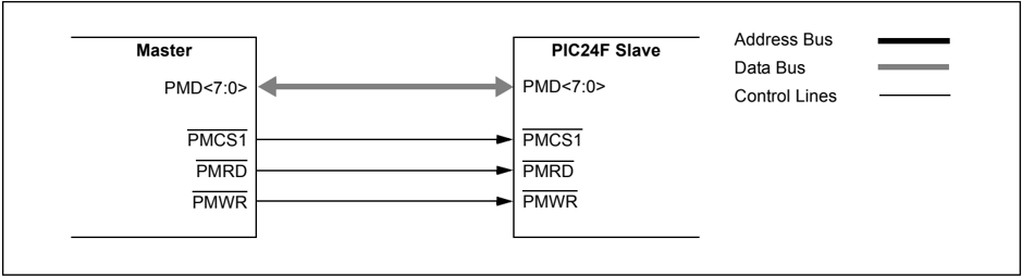
FIGURE 18-3: ADDRESSABLE PARALLEL SLAVE PORT EXAMPLE
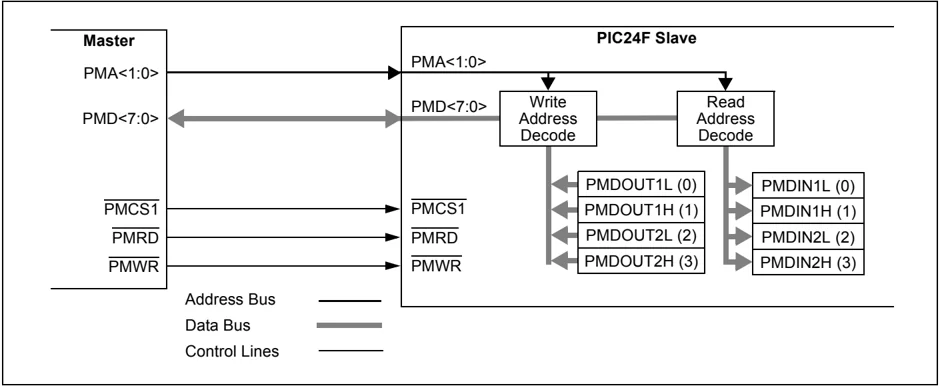
TABLE 18-1: SLAVE MODE ADDRESS RESOLUTION
| PMA<1:0> | Output Register (Buffer) | Input Register (Buffer) |
|---|---|---|
| 00 | PMDOUT1<7:0> (0) | PMDIN1<7:0> (0) |
| 01 | PMDOUT1<15:8> (1) | PMDIN1<15:8> (1) |
| 10 | PMDOUT2<7:0> (2) | PMDIN2<7:0> (2) |
| 11 | PMDOUT2<15:8> (3) | PMDIN2<15:8> (3) |
FIGURE 18-4: MASTER MODE, DEMULTIPLEXED ADDRESSING (SEPARATE READ AND WRITE STROBES, SINGLE CHIP SELECT)
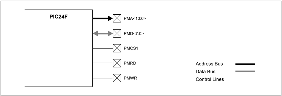
FIGURE 18-5: MASTER MODE, PARTIALLY MULTIPLEXED ADDRESSING (SEPARATE READ AND WRITE STROBES, SINGLE CHIP SELECT)
 PIC24F
PMA<10:8>
PMD<7:0>
PMA<7:0>
PMCS1
PMALL
PMRD
PMWR
Address Bus Multiplexed Data and Address Bus Control Lines
FIGURE 18-6: MASTER MODE, FULLY MULTIPLEXED ADDRESSING (SEPARATE READ AND WRITE STROBES, SINGLE CHIP SELECT)
 PIC24F
PMD<7:0>
PMA<7:0>
PMA<15:8>
PMCS1
PMALL
PMALH
PMRD
PMWR
Multiplexed Data and Address Bus Control Lines
FIGURE 18-7: EXAMPLE OF A MULTIPLEXED ADDRESSING APPLICATION
 PIC24F
PMD<7:0>
PMALL
373
A<7:0>
D<7:0>
A<15:0>
D<7:0>
CE
OE
WR
373
A<15:8>
PMALH
PMCS1
PMRD
PMWR
Address Bus Data Bus Control Lines
FIGURE 18-8: EXAMPLE OF A PARTIALLY MULTIPLEXED ADDRESSING APPLICATION
 PIC24F
PMD<7:0>
PMALL
373
A<7:0>
D<7:0>
A<10:0>
D<7:0>
CE
OE
WR
A<10:8>
PMA<10:8>
PMCS1
PMRD
PMWR
Address Bus Data Bus Control Lines
FIGURE 18-9: EXAMPLE OF AN 8-BIT MULTIPLEXED ADDRESS AND DATA APPLICATION
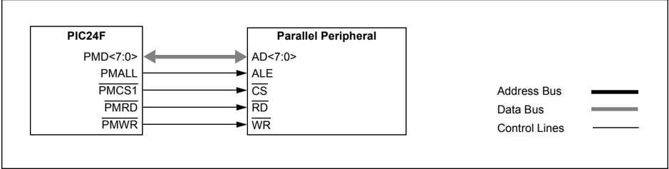
FIGURE 18-10: PARALLEL EEPROM EXAMPLE (UP TO 11-BIT ADDRESS, 8-BIT DATA)
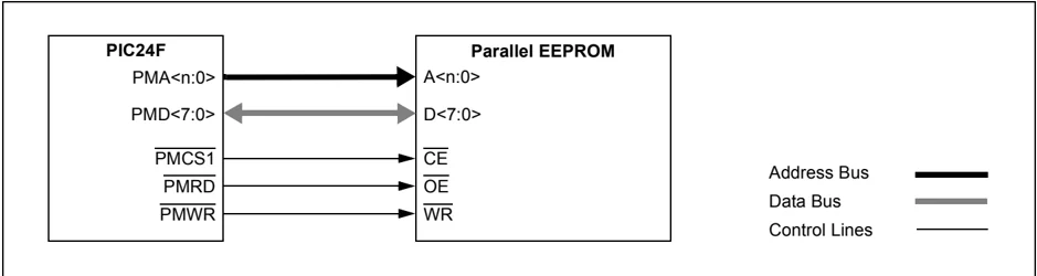
FIGURE 18-11: PARALLEL EEPROM EXAMPLE (UP TO 11-BIT ADDRESS, 16-BIT DATA)
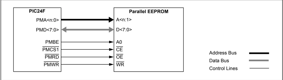
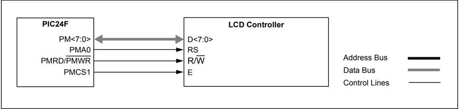
FIGURE 18-12: LCD CONTROL EXAMPLE (BYTE MODE OPERATION)
19.0 REAL-TIME CLOCK AND CALENDAR (RTCC)
Note: This data sheet summarizes the features of this group of PIC24F devices. It is not intended to be a comprehensive reference source. For more information, refer to the "PIC24F Family Reference Manual", "Real-Time Clock and Calendar (RTCC)" (DS39696).
The Real-Time Clock and Calendar (RTCC) provides on-chip, hardware-based clock and calendar functionality with little or no CPU overhead. It is intended for applications where accurate time must be maintained for extended periods, with minimal CPU activity and with limited power resources, such as battery-powered applications.
Key features include:
- Time data in hours, minutes and seconds, with a granularity of one-half second
- 24-hour format (military time) display option
- Calendar data as date, month and year
- Automatic, hardware-based day of week and leap year calculations for dates from 2000 through 2099
- Time and calendar data in BCD format for compact firmware
- Highly configurable alarm function
- External output pin with selectable alarm signal or seconds "tick" signal output
- Time base input from Secondary Oscillator (SOSC) or the T1CK digital clock input (32.768 kHz)
- User calibration feature with auto-adjust
A simplified block diagram of the module is shown in Figure 19-1. The SOSC and RTCC will both remain running while the device is held in Reset with MCLR, and will continue running after MCLR is released.
FIGURE 19-1: RTCC BLOCK DIAGRAM
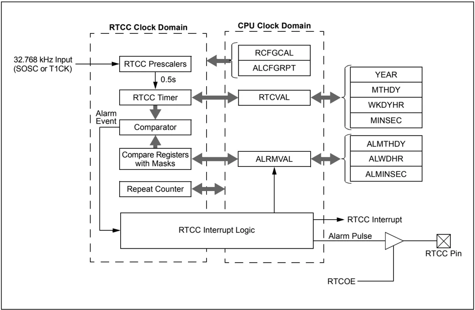
19.1 RTCC Module Registers
The RTCC module registers are organized into three categories:
- RTCC Control Registers
- RTCC Value Registers
- Alarm Value Registers
19.1.1 REGISTER MAPPING
To limit the register interface, the RTCC Timer and Alarm Time registers are accessed through corresponding register pointers. The RTCC Value register window (RTCVALH and RTCVALL) uses the RTCPTR<1:0> bits (RCFGCAL<9:8>) to select the desired Timer register pair (see Table 19-1).
By writing the RTCVALH byte, the RTCC Pointer value (the RTCPTR<1:0> bits) decrements by one until the bits reach '00'. Once they reach '00', the MINUTES and SECONDS value will be accessible through RTCVALH and RTCVALL until the pointer value is manually changed.
TABLE 19-1: RTCVAL REGISTER MAPPING
The Alarm Value register window (ALRMVALH and ALRMVALL) uses the ALRMPTR bits (ALCFGRCT<9:8>) to select the desired Alarm register pair (see Table 19-2).
By writing the ALRMVALH byte, the Alarm Pointer value (the ALRMPTR<1:0> bits) decrements by one until the bits reach '00'. Once they reach '00', the ALRMMIN and ALRMSEC value will be accessible through ALRMVALH and ALRMVALL until the pointer value is manually changed.
TABLE 19-2: ALRMVAL REGISTER MAPPING
Considering that the 16-bit core does not distinguish between 8-bit and 16-bit read operations, the user must be aware that when reading either the ALRMVALH or ALRMVALL, the bytes will decrement the ALRMPTR<1:0> value. The same applies to the RTCVALH or RTCVALL bytes with the RTCPTR<1:0> being decremented.
Note: This only applies to read operations and not write operations.
19.1.2 WRITE LOCK
In order to perform a write to any of the RTCC Timer registers, the RTCWREN bit (RCFGCAL<13>) must be set (refer to Example 19-1).
Note: To avoid accidental writes to the timer, it is recommended that the RTCWREN bit (RCFGCAL<13>) is kept clear at any other time. For the RTCWREN bit to be set, there is only 1 instruction cycle time window allowed between the 55h/AA sequence and the setting of RTCWREN; therefore, it is recommended that code follow the procedure in Example 19-1.
EXAMPLE 19-1: SETTING THE RTCWREN BIT
asm volatile("push w7"); asm volatile("push w8"); asm volatile("disi #5"); asm volatile("mov #0x55, w7"); asm volatile("mov w7, _NVMKEY"); asm volatile("mov #0xAA, w8"); asm volatile("mov w8, _NVMKEY"); asm volatile("bset _RCFGCAL, #13"); //set the RTCWREN bit asm volatile("pop w8"); asm volatile("pop w7");
19.1.3 RTCC CONTROL REGISTERS
REGISTER 19-1: RCFGCAL: RTCC CALIBRATION AND CONFIGURATION REGISTER(1)
| R/W-0 | U-0 | R/W-0 | R-0 | R-0 | R/W-0 | R/W-0 | R/W-0 |
|---|---|---|---|---|---|---|---|
| RTCEN(2) | — | RTCWREN | RTCSYNC | HALFSEC(3) | RTCOE | RTCPTR1 | RTCPTR0 |
| bit 15 | bit 8 |
| R/W-0 | R/W-0 | R/W-0 | R/W-0 | R/W-0 | R/W-0 | R/W-0 | R/W-0 |
|---|---|---|---|---|---|---|---|
| CAL7 | CAL6 | CAL5 | CAL4 | CAL3 | CAL2 | CAL1 | CAL0 |
| bit 7 | bit 0 |
Legend:
R = Readable bit
W = Writable bit
U = Unimplemented bit, read as ‘0’
-n = Value at POR
‘1’ = Bit is set
‘0’ = Bit is cleared
x = Bit is unknown
bit 15
RTCEN: RTCC Enable bit(2)
1 = RTCC module is enabled
0 = RTCC module is disabled
bit 14
Unimplemented: Read as ‘0’
bit 13
RTCWREN: RTCC Value Registers Write Enable bit
1 = RTCVALH and RTCVALL registers can be written to by the user
0 = RTCVALH and RTCVALL registers are locked out from being written to by the user
bit 12
RTCSYNC: RTCC Value Registers Read Synchronization bit
1 = RTCVALH, RTCVALL and ALCFGRPT registers can change while reading due to a rollover ripple resulting in an invalid data read. If the register is read twice and results in the same data, the data can be assumed to be valid.
0 = RTCVALH, RTCVALL or ALCFGRPT register can be read without concern over a rollover ripple
bit 11
HALFSEC: Half-Second Status bit(3)
1 = Second half period of a second
0 = First half period of a second
bit 10
RTCOE: RTCC Output Enable bit
1 = RTCC output is enabled
0 = RTCC output is disabled
bit 9-8
RTCPTR<1:0>: RTCC Value Register Window Pointer bits
Points to the corresponding RTCC Value registers when reading the RTCVALH and RTCVALL registers; the RTCPTR<1:0> value decrements on every read or write of RTCVALH until it reaches ‘00’.
RTCVAL<15:8>:
00 = MINUTES
01 = WEEKDAY
10 = MONTH
11 = Reserved
RTCVAL<7:0>:
00 = SECONDS
01 = HOURS
10 = DAY
11 = YEAR
Note 1: The RCFGCAL register is only affected by a POR.
2: A write to the RTCEN bit is only allowed when RTCWREN = 1.
3: This bit is read-only. It is cleared to ‘0’ on a write to the lower half of the MINSEC register.
REGISTER 19-1: RCFGCAL: RTCC CALIBRATION AND CONFIGURATION REGISTER⁽¹⁾
bit 7-0
CAL<7:0>: RTCC Drift Calibration bits
01111111 = Maximum positive adjustment; adds 508 RTC clock pulses every one minute
...
01111111 = Minimum positive adjustment; adds 4 RTC clock pulses every one minute
00000000 = No adjustment
11111111 = Minimum negative adjustment; subtracts 4 RTC clock pulses every one minute
...
10000000 = Maximum negative adjustment; subtracts 512 RTC clock pulses every one minute
Note 1: The RCFGCAL register is only affected by a POR.
2: A write to the RTCEN bit is only allowed when RTCWREN = 1.
3: This bit is read-only. It is cleared to ‘0’ on a write to the lower half of the MINSEC register.
REGISTER 19-2: PADC FG1: PAD CONFIGURATION CONTROL REGISTER
| U-0 | U-0 | U-0 | U-0 | U-0 | U-0 | U-0 | U-0 |
|---|---|---|---|---|---|---|---|
| — | — | — | — | — | — | — | — |
| bit 15 | bit 8 |
| U-0 | U-0 | U-0 | U-0 | U-0 | U-0 | R/W-0 | R/W-0 |
|---|---|---|---|---|---|---|---|
| — | — | — | — | — | — | RTSECS EL⁽¹⁾ | PMPTTL |
| bit 7 | bit 0 |
Legend:
R = Readable bit
W = Writable bit
U = Unimplemented bit, read as ‘0’
-n = Value at POR
‘1’ = Bit is set
‘0’ = Bit is cleared
x = Bit is unknown
bit 15-2
Unimplemented: Read as ‘0’
bit 1
RTSECS EL: RTCC Seconds Clock Output Select bit⁽¹⁾
1 = RTCC seconds clock is selected for the RTCC pin
0 = RTCC alarm pulse is selected for the RTCC pin
bit 0
PMPTTL: PMP Module TTL Input Buffer Select bit
1 = PMP module uses TTL input buffers
0 = PMP module uses Schmitt Trigger input buffers
Note 1: To enable the actual RTCC output, the RTCOE (RCFGCAL) bit needs to be set.
REGISTER 19-3: ALCFGRPT: ALARM CONFIGURATION REGISTER
| R/W-0 | R/W-0 | R/W-0 | R/W-0 | R/W-0 | R/W-0 | R/W-0 | R/W-0 |
|---|---|---|---|---|---|---|---|
| ALRMEN | CHIME | AMASK3 | AMASK2 | AMASK1 | AMASK0 | ALRMPTR1 | ALRMPTR0 |
| bit 15 | bit 8 |
| R/W-0 | R/W-0 | R/W-0 | R/W-0 | R/W-0 | R/W-0 | R/W-0 | R/W-0 |
|---|---|---|---|---|---|---|---|
| ARPT7 | ARPT6 | ARPT5 | ARPT4 | ARPT3 | ARPT2 | ARPT1 | ARPT0 |
| bit 7 | bit 0 |
Legend:
R = Readable bit
W = Writable bit
U = Unimplemented bit, read as ‘0’
-n = Value at POR
‘1’ = Bit is set
‘0’ = Bit is cleared
x = Bit is unknown
bit 15
ALRMEN: Alarm Enable bit
1 = Alarm is enabled (cleared automatically after an alarm event whenever ARPT<7:0> = 00h and CHIME = 0)
0 = Alarm is disabled
bit 14
CHIME: Chime Enable bit
1 = Chime is enabled; ARPT<7:0> bits are allowed to roll over from 00h to FFh
0 = Chime is disabled; ARPT<7:0> bits stop once they reach 00h
bit 13-10
AMASK<3:0>: Alarm Mask Configuration bits
0000 = Every half second
0001 = Every second
0010 = Every 10 seconds
0011 = Every minute
0100 = Every 10 minutes
0101 = Every hour
0110 = Once a day
0111 = Once a week
1000 = Once a month
1001 = Once a year (except when configured for February 29th, once every 4 years)
101x = Reserved; do not use
11xx = Reserved; do not use
bit 9-8
ALRMPTR<1:0>: Alarm Value Register Window Pointer bits
Points to the corresponding Alarm Value registers when reading ALRMVALH and ALRMVALL registers; the ALRMPTR<1:0> value decrements on every read or write of ALRMVALH until it reaches ‘00’.
ALRMVAL<15:8>:
00 = ALRMMIN
01 = ALRMWD
10 = ALRMMNTH
11 = Unimplemented
ALRMVAL<7:0>:
00 = ALRMSEC
01 = ALRMHR
10 = ALRMDAY
11 = Unimplemented
bit 7-0
ARPT<7:0>: Alarm Repeat Counter Value bits
11111111 = Alarm will repeat 255 more times
...
00000000 = Alarm will not repeat
The counter decrements on any alarm event. The counter is prevented from rolling over from 00h to FFh unless CHIME = 1.
19.1.4 RTCVAL REGISTER MAPPINGS
REGISTER 19-4: YEAR: YEAR VALUE REGISTER(1)
| U-0 | U-0 | U-0 | U-0 | U-0 | U-0 | U-0 | U-0 |
|---|---|---|---|---|---|---|---|
| — | — | — | — | — | — | — | — |
| bit 15 | bit 8 |
| R/W-x | R/W-x | R/W-x | R/W-x | R/W-x | R/W-x | R/W-x | R/W-x |
|---|---|---|---|---|---|---|---|
| YRTEN3 | YRTEN2 | YRTEN1 | YRTEN0 | YRONE3 | YRONE2 | YRONE1 | YRONE0 |
| bit 7 | bit 0 |
Legend: R = Readable bit W = Writable bit U = Unimplemented bit, read as ‘0’ -n = Value at POR ‘1’ = Bit is set ‘0’ = Bit is cleared x = Bit is unknown
bit 15-8 Unimplemented: Read as ‘0’ bit 7-4 YRTEN<3:0>: Binary Coded Decimal Value of Year’s Tens Digit bits Contains a value from 0 to 9. bit 3-0 YRONE<3:0>: Binary Coded Decimal Value of Year’s Ones Digit bits Contains a value from 0 to 9.
Note 1: A write to this register is only allowed when RTCWREN = 1.
REGISTER 19-5: MTHDY: MONTH AND DAY VALUE REGISTER(1)
| U-0 | U-0 | U-0 | R-x | R-x | R-x | R-x | R-x |
|---|---|---|---|---|---|---|---|
| — | — | — | MTHTEN0 | MTHONE3 | MTHONE2 | MTHONE1 | MTHONE0 |
| bit 15 | bit 8 |
| U-0 | U-0 | R/W-x | R/W-x | R/W-x | R/W-x | R/W-x | R/W-x |
|---|---|---|---|---|---|---|---|
| — | — | DAYTEN1 | DAYTEN0 | DAYONE3 | DAYONE2 | DAYONE1 | DAYONE0 |
| bit 7 | bit 0 |
Legend: R = Readable bit W = Writable bit U = Unimplemented bit, read as ‘0’ -n = Value at POR ‘1’ = Bit is set ‘0’ = Bit is cleared x = Bit is unknown
bit 15-13 Unimplemented: Read as ‘0’ bit 12 MTHTEN0: Binary Coded Decimal Value of Month’s Tens Digit bit Contains a value of ‘0’ or ‘1’. bit 11-8 MTHONE<3:0<: Binary Coded Decimal Value of Month’s Ones Digit bits Contains a value from 0 to 9. bit 7-6 Unimplemented: Read as ‘0’ bit 5-4 DAYTEN<1:0>: Binary Coded Decimal Value of Day’s Tens Digit bits Contains a value from 0 to 3. bit 3-0 DAYONE<3:0>: Binary Coded Decimal Value of Day’s Ones Digit bits Contains a value from 0 to 9.
Note 1: A write to this register is only allowed when RTCWREN = 1.
REGISTER 19-6: WKDYHR: WEEKDAY AND HOURS VALUE REGISTER(1)
| U-0 | U-0 | U-0 | U-0 | U-0 | R/W-x | R/W-x | R/W-x |
|---|---|---|---|---|---|---|---|
| — | — | — | — | — | WDAY2 | WDAY1 | WDAY0 |
| bit 15 | bit 8 |
| U-0 | U-0 | R/W-x | R/W-x | R/W-x | R/W-x | R/W-x | R/W-x |
|---|---|---|---|---|---|---|---|
| — | — | HRTEN1 | HRTEN0 | HRONE3 | HRONE2 | HRONE1 | HRONE0 |
| bit 7 | bit 0 |
Legend:
R = Readable bit
W = Writable bit
U = Unimplemented bit, read as ‘0’
-n = Value at POR
‘1’ = Bit is set
‘0’ = Bit is cleared
x = Bit is unknown
- bit 15-11 Unimplemented: Read as ‘0’
- bit 10-8 WDAY<2:0>: Binary Coded Decimal Value of Weekday Digit bits
Contains a value from 0 to 6. - bit 7-6 Unimplemented: Read as ‘0’
- bit 5-4 HRTEN<1:0>: Binary Coded Decimal Value of Hour’s Tens Digit bits
Contains a value from 0 to 2. - bit 3-0 HRONE<3:0>: Binary Coded Decimal Value of Hour’s Ones Digit bits
Contains a value from 0 to 9.
Note 1: A write to this register is only allowed when RTCWREN = 1.
REGISTER 19-7: MINSEC: MINUTES AND SECONDS VALUE REGISTER
| U-0 | R/W-x | R/W-x | R/W-x | R/W-x | R/W-x | R/W-x | R/W-x |
|---|---|---|---|---|---|---|---|
| — | MINTEN2 | MINTEN1 | MINTEN0 | MINONE3 | MINONE2 | MINONE1 | MINONE0 |
| bit 15 | bit 8 |
| U-0 | R/W-x | R/W-x | R/W-x | R/W-x | R/W-x | R/W-x | R/W-x |
|---|---|---|---|---|---|---|---|
| — | SECTEN2 | SECTEN1 | SECTEN0 | SECON3 | SECON2 | SECON1 | SECON0 |
| bit 7 | bit 0 |
Legend:
R = Readable bit
W = Writable bit
U = Unimplemented bit, read as ‘0’
-n = Value at POR
‘1’ = Bit is set
‘0’ = Bit is cleared
x = Bit is unknown
- bit 15 Unimplemented: Read as ‘0’
- bit 14-12 MINTEN<2:0>: Binary Coded Decimal Value of Minute’s Tens Digit bits
Contains a value from 0 to 5. - bit 11-8 MINONE<3:0>: Binary Coded Decimal Value of Minute’s Ones Digit bits
Contains a value from 0 to 9. - bit 7 Unimplemented: Read as ‘0’
- bit 6-4 SECTEN<2:0>: Binary Coded Decimal Value of Second’s Tens Digit bits
Contains a value from 0 to 5. - bit 3-0 SECON<3:0>: Binary Coded Decimal Value of Second’s Ones Digit bits
Contains a value from 0 to 9.
19.1.5 ALRMVAL REGISTER MAPPINGS
REGISTER 19-8: ALMTHDY: ALARM MONTH AND DAY VALUE REGISTER(1)
| U-0 | U-0 | U-0 | R/W-x | R/W-x | R/W-x | R/W-x | R/W-x |
|---|---|---|---|---|---|---|---|
| — | — | — | MTHTEN0 | MTHONE3 | MTHONE2 | MTHONE1 | MTHONE0 |
| bit 15 | bit 8 |
| U-0 | U-0 | R/W-x | R/W-x | R/W-x | R/W-x | R/W-x | R/W-x |
|---|---|---|---|---|---|---|---|
| — | — | DAYTEN1 | DAYTEN0 | DAYONE3 | DAYONE2 | DAYONE1 | DAYONE0 |
| bit 7 | bit 0 |
Legend: R = Readable bit W = Writable bit U = Unimplemented bit, read as ‘0’ -n = Value at POR ‘1’ = Bit is set ‘0’ = Bit is cleared x = Bit is unknown
bit 15-13 Unimplemented: Read as ‘0’ bit 12 MTHTEN0: Binary Coded Decimal Value of Month’s Tens Digit bit Contains a value of ‘0’ or ‘1’. bit 11-8 MTHONE<3:0>: Binary Coded Decimal Value of Month’s Ones Digit bits Contains a value from 0 to 9. bit 7-6 Unimplemented: Read as ‘0’ bit 5-4 DAYTEN<1:0>: Binary Coded Decimal Value of Day’s Tens Digit bits Contains a value from 0 to 3. bit 3-0 DAYONE<3:0>: Binary Coded Decimal Value of Day’s Ones Digit bits Contains a value from 0 to 9.
Note 1: A write to this register is only allowed when RTCWREN = 1.
REGISTER 19-9: ALWDHR: ALARM WEEKDAY AND HOURS VALUE REGISTER(1)
| U-0 | U-0 | U-0 | U-0 | U-0 | R/W-x | R/W-x | R/W-x |
|---|---|---|---|---|---|---|---|
| — | — | — | — | — | WDAY2 | WDAY1 | WDAY0 |
| bit 15 | bit 8 |
| U-0 | U-0 | R/W-x | R/W-x | R/W-x | R/W-x | R/W-x | R/W-x |
|---|---|---|---|---|---|---|---|
| — | — | HRTEN1 | HRTEN0 | HRONE3 | HRONE2 | HRONE1 | HRONE0 |
| bit 7 | bit 0 |
Legend:
R = Readable bit
W = Writable bit
U = Unimplemented bit, read as ‘0’
-n = Value at POR
‘1’ = Bit is set
‘0’ = Bit is cleared
x = Bit is unknown
bit 15-11 Unimplemented: Read as ‘0’
bit 10-8 WDAY<2:0>: Binary Coded Decimal Value of Weekday Digit bits
Contains a value from 0 to 6.
bit 7-6 Unimplemented: Read as ‘0’
bit 5-4 HRTEN<1:0>: Binary Coded Decimal Value of Hour’s Tens Digit bits
Contains a value from 0 to 2.
bit 3-0 HRONE<3:0>: Binary Coded Decimal Value of Hour’s Ones Digit bits
Contains a value from 0 to 9.
Note 1: A write to this register is only allowed when RTCWREN = 1.
REGISTER 19-10: ALMINSEC: ALARM MINUTES AND SECONDS VALUE REGISTER
| U-0 | R/W-x | R/W-x | R/W-x | R/W-x | R/W-x | R/W-x | R/W-x |
|---|---|---|---|---|---|---|---|
| — | MINTEN2 | MINTEN1 | MINTEN0 | MINONE3 | MINONE2 | MINONE1 | MINONE0 |
| bit 15 | bit 8 |
| U-0 | R/W-x | R/W-x | R/W-x | R/W-x | R/W-x | R/W-x | R/W-x |
|---|---|---|---|---|---|---|---|
| — | SECTEN2 | SECTEN1 | SECTEN0 | SECON3 | SECON2 | SECON1 | SECON0 |
| bit 7 | bit 0 |
Legend:
R = Readable bit
W = Writable bit
U = Unimplemented bit, read as ‘0’
-n = Value at POR
‘1’ = Bit is set
‘0’ = Bit is cleared
x = Bit is unknown
bit 15 Unimplemented: Read as ‘0’
bit 14-12 MINTEN<2:0>: Binary Coded Decimal Value of Minute’s Tens Digit bits
Contains a value from 0 to 5.
bit 11-8 MINONE<3:0>: Binary Coded Decimal Value of Minute’s Ones Digit bits
Contains a value from 0 to 9.
bit 7 Unimplemented: Read as ‘0’
bit 6-4 SECTEN<2:0>: Binary Coded Decimal Value of Second’s Tens Digit bits
Contains a value from 0 to 5.
bit 3-0 SECON<3:0>: Binary Coded Decimal Value of Second’s Ones Digit bits
Contains a value from 0 to 9.
19.2 Calibration
The real-time crystal input can be calibrated using the periodic auto-adjust feature. When properly calibrated, the RTCC can provide an error of less than 3 seconds per month. This is accomplished by finding the number of error clock pulses and storing the value into the lower half of the RCFGCAL register. The 8-bit signed value, loaded into the lower half of RCFGCAL, is multiplied by four and will be either added or subtracted from the RTCC timer, once every minute. Refer to the steps below for RTCC calibration:
- Using another timer resource on the device, the user must find the error of the 32.768 kHz crystal.
- Once the error is known, it must be converted to the number of error clock pulses per minute.
EQUATION 19-1:
(Ideal Frequency† – Measured Frequency) * 60 = Clocks per Minute † Ideal frequency = 32,768 Hz
- a) If the oscillator is faster then ideal (negative result form Step 2), the RCFGCAL register value needs to be negative. This causes the specified number of clock pulses to be subtracted from the timer counter, once every minute. b) If the oscillator is slower then ideal (positive result from Step 2), the RCFGCAL register value needs to be positive. This causes the specified number of clock pulses to be subtracted from the timer counter, once every minute.
- Divide the number of error clocks per minute by 4 to get the correct CAL<7:0> bits value and load the RCFGCAL register with the correct value.
(Each 1-bit increment in the CALx bits value adds or subtracts 4 pulses).
Writes to the lower half of the RCFGCAL register should only occur when the timer is turned off or immediately after the rising edge of the seconds pulse.
Note: It is up to the user to include in the error value the initial error of the crystal, drift due to temperature and drift due to crystal aging.
19.3 Alarm
- Configurable from half second to one year
- Enabled using the ALRMEN bit (ALCFGRPT<15>, Register 19-3)
- One-time alarm and repeat alarm options are available
19.3.1 CONFIGURING THE ALARM
The alarm feature is enabled using the ALRMEN bit. This bit is cleared when an alarm is issued. Writes to ALRMVAL should only take place when ALRMEN = 0.
As shown in Figure 19-2, the interval selection of the alarm is configured through the AMASK<3:0> bits (ALCFGRPT<13:10>). These bits determine which and how many digits of the alarm must match the clock value for the alarm to occur.
The alarm can also be configured to repeat based on a preconfigured interval. The amount of times this occurs, once the alarm is enabled, is stored in the ARPT<7:0> bits (ALCFGRPT<7:0>). When the value of the ARPTx bits equals 00h and the CHIME bit (ALCFGRPT<14>) is cleared, the repeat function is disabled and only a single alarm will occur. The alarm can be repeated up to 255 times by loading ARPT<7:0> with FFh.
After each alarm is issued, the value of the ARPTx bits is decremented by one. Once the value has reached 00h, the alarm will be issued one last time, after which, the ALRMEN bit will be cleared automatically and the alarm will turn off.
Indefinite repetition of the alarm can occur if CHIME (ALCFGRPT<14>) = 1. Instead of the alarm being disabled when the value of the ARPTX bits reaches 00h, it rolls over to FFh and continues counting indefinitely while CHIME is set.
19.3.2 ALARM INTERRUPT
At every alarm event, an interrupt is generated. In addition, an alarm pulse output is provided that operates at half the frequency of the alarm. This output is completely synchronous to the RTCC clock and can be used as a trigger clock to other peripherals.
Note: Changing any of the registers, other then the RCFGCAL and ALCFGRPT registers and the CHIME bit while the alarm is enabled (ALRMEN = 1), can result in a false alarm event leading to a false alarm interrupt. To avoid a false alarm event, the timer and alarm values should only be changed while the alarm is disabled (ALRMEN = 0). It is recommended that the ALCFGRPT register and CHIME bit be changed when RTCSYNC = 0.
FIGURE 19-2: ALARM MASK SETTINGS
| Alarm Mask Setting (AMASK<3:0>) | Day of the Week | Month | Day | Hours | Minutes | Seconds |
|---|---|---|---|---|---|---|
| 0000 – Every half second | □ | □□/□□ | □□ | □□:□□:□□ | ||
| 0001 – Every second | □ | □□/□□ | □□ | □□:□□:□□ | ||
| 0010 – Every 10 seconds | □ | □□/□□ | □□ | □□:□□:□s | ||
| 0011 – Every minute | □ | □□/□□ | □□ | □□:□□:ss | ||
| 0100 – Every 10 minutes | □ | □□/□□ | □□ | □□:□m:ss | ||
| 0101 – Every hour | □ | □□/□□ | □□ | □□:mm:ss | ||
| 0110 – Every day | □ | □□/□□ | □□ | hh:mm:ss | ||
| 0111 – Every week | d | □□/□□ | □□ | hh:mm:ss | ||
| 1000 – Every month | □ | □□/dd | □□ | hh:mm:ss | ||
| 1001 – Every year(1) | □ | mm/dd | □□ | hh:mm:ss |
Note 1: Annually, except when configured for February 29.
NOTES:
DS39881E-page 188 © 2010-2013 Microchip Technology Inc.