5.0 FLASH PROGRAM MEMORY
Note: This data sheet summarizes the features of this group of PIC24F devices. It is not intended to be a comprehensive reference source. For more information, refer to the "PIC24F Family Reference Manual", "Program Memory" (DS39715).
The PIC24FJ64GA004 family of devices contains internal Flash program memory for storing and executing application code. The memory is readable, writable and erasable when operating with VDD over 2.25V.
Flash memory can be programmed in three ways:
- In-Circuit Serial Programming™ (ICSP™)
- Run-Time Self-Programming (RTSP)
- Enhanced In-Circuit Serial Programming (Enhanced ICSP)
ICSP allows a PIC24FJ64GA004 family device to be serially programmed while in the end application circuit. This is simply done with two lines for the programming clock and programming data (which are named PGCx and PGDx, respectively), and three other lines for power (VDD), ground (VSS) and Master Clear (MCLR). This allows customers to manufacture boards with unprogrammed devices and then program the microcontroller just before shipping the product. This also allows the most recent firmware or a custom firmware to be programmed.
RTSP is accomplished using TBLRD (Table Read) and TBLWT (Table Write) instructions. With RTSP, the user may write program memory data in blocks of 64 instructions (192 bytes) at a time and erase program memory in blocks of 512 instructions (1536 bytes) at a time.
5.1 Table Instructions and Flash Programming
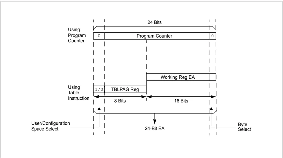
Regardless of the method used, all programming of Flash memory is done with the table read and table write instructions. These allow direct read and write access to the program memory space from the data memory while the device is in normal operating mode. The 24-bit target address in the program memory is formed using the TBLPAG<7:0> bits and the Effective Address (EA) from a W register, specified in the table instruction, as shown in Figure 5-1.
The TBLRDL and the TBLWTL instructions are used to read or write to bits<15:0> of program memory. TBLRDL and TBLWTL can access program memory in both Word and Byte modes.
The TBLRDH and TBLWTH instructions are used to read or write to bits<23:16> of program memory. TBLRDH and TBLWTH can also access program memory in Word or Byte mode.
FIGURE 5-1: ADDRESSING FOR TABLE REGISTERS
5.2 RTSP Operation
The PIC24F Flash program memory array is organized into rows of 64 instructions or 192 bytes. RTSP allows the user to erase blocks of eight rows (512 instructions) at a time and to program one row at a time. It is also possible to program single words.
The 8-row erase blocks and single row write blocks are edge-aligned, from the beginning of program memory, on boundaries of 1536 bytes and 192 bytes, respectively.
When data is written to program memory using TBLWT instructions, the data is not written directly to memory. Instead, data written using table writes is stored in holding latches until the programming sequence is executed.
Any number of TBLWT instructions can be executed and a write will be successfully performed. However, 64 TBLWT instructions are required to write the full row of memory.
To ensure that no data is corrupted during a write, any unused addresses should be programmed with FFFFFFh. This is because the holding latches reset to an unknown state, so if the addresses are left in the Reset state, they may overwrite the locations on rows which were not rewritten.
The basic sequence for RTSP programming is to set up a Table Pointer, then do a series of TBLWT instructions to load the buffers. Programming is performed by setting the control bits in the NVMCON register.
Data can be loaded in any order and the holding registers can be written to multiple times before performing a write operation. Subsequent writes, however, will wipe out any previous writes.
Note: Writing to a location multiple times without erasing it is not recommended.
All of the table write operations are single-word writes (2 instruction cycles), because only the buffers are written. A programming cycle is required for programming each row.
5.3 Enhanced In-Circuit Serial Programming
Enhanced In-Circuit Serial Programming uses an on-board bootloader, known as the Program Executive (PE), to manage the programming process. Using an SPI data frame format, the Program Executive can erase, program and verify program memory. For more information on Enhanced ICSP, see the device programming specification.
5.4 Control Registers
There are two SFRs used to read and write the program Flash memory: NVMCON and NVMKEY.
The NVMCON register (Register 5-1) controls which blocks are to be erased, which memory type is to be programmed and when the programming cycle starts.
NVMKEY is a write-only register that is used for write protection. To start a programming or erase sequence, the user must consecutively write 55h and AAh to the NVMKEY register. Refer to Section 5.5 “Programming Operations” for further details.
5.5 Programming Operations
A complete programming sequence is necessary for programming or erasing the internal Flash in RTSP mode. During a programming or erase operation, the processor stalls (waits) until the operation is finished. Setting the WR bit (NVMCON<15>) starts the operation and the WR bit is automatically cleared when the operation is finished.
Configuration Word values are stored in the last two locations of program memory. Performing a page erase operation on the last page of program memory clears these values and enables code protection. As a result, avoid performing page erase operations on the last page of program memory.
REGISTER 5-1: NVMCON: FLASH MEMORY CONTROL REGISTER
| R/SO-0 | R/W-0 | R/W-0 | U-0 | U-0 | U-0 | U-0 | U-0 |
|---|---|---|---|---|---|---|---|
| WR | WREN | WRERR | — | — | — | — | — |
| bit 15 | bit 8 |
| U-0 | R/W-0 | U-0 | U-0 | R/W-0 | R/W-0 | R/W-0 | R/W-0 |
|---|---|---|---|---|---|---|---|
| — | ERASE | — | — | NVMOP3⁽¹⁾ | NVMOP2⁽¹⁾ | NVMOP1⁽¹⁾ | NVMOP0⁽¹⁾ |
| bit 7 | bit 0 |
Legend:
- R = Readable bit
- W = Writable bit
- U = Unimplemented bit, read as ‘0’
- -n = Value at POR
- ‘1’ = Bit is set
- ‘0’ = Bit is cleared
- x = Bit is unknown
- SO = Settable Only bit
bit 15
WR: Write Control bit
1 = Initiates a Flash memory program or erase operation; the operation is self-timed and the bit is cleared by hardware once operation is complete
0 = Program or erase operation is complete and inactive
bit 14
WREN: Write Enable bit
1 = Enables Flash program/erase operations
0 = Inhibits Flash program/erase operations
bit 13
WRERR: Write Sequence Error Flag bit
1 = An improper program or erase sequence attempt or termination has occurred (bit is set automatically on any set attempt of the WR bit)
0 = The program or erase operation completed normally
bit 12-7
Unimplemented: Read as ‘0’
bit 6
ERASE: Erase/Program Enable bit
1 = Performs the erase operation specified by the NVMOP<3:0> bits on the next WR command
0 = Performs the program operation specified by the NVMOP<3:0> bits on the next WR command
bit 5-4
Unimplemented: Read as ‘0’
bit 3-0
NVMOP<3:0>: NVM Operation Select bits⁽¹⁾
1111 = Memory bulk erase operation (ERASE = 1) or no operation (ERASE = 0)⁽²⁾
0011 = Memory word program operation (ERASE = 0) or no operation (ERASE = 1)
0010 = Memory page erase operation (ERASE = 1) or no operation (ERASE = 0)
0001 = Memory row program operation (ERASE = 0) or no operation (ERASE = 1)
Note 1: All other combinations of NVMOP<3:0> are unimplemented.
Note 2: Available in ICSP™ mode only. Refer to the device programming specifications.
5.5.1 PROGRAMMING ALGORITHM FOR FLASH PROGRAM MEMORY
The user can program one row of Flash program memory at a time. To do this, it is necessary to erase the 8-row erase block containing the desired row. The general process is:
- Read eight rows of program memory (512 instructions) and store in data RAM.
- Update the program data in RAM with the desired new data.
- Erase the block (see Example 5-1): a) Set the NVMOPx bits (NVMCON<3:0>) to '0010' to configure for block erase. Set the ERASE (NVMCON<6>) and WREN (NVMCON<14>) bits. b) Write the starting address of the block to be erased into the TBLPAG and W registers. c) Write 55h to NVMKEY. d) Write AAh to NVMKEY. e) Set the WR bit (NVMCON<15>). The erase cycle begins and the CPU stalls for the duration of the erase cycle. When the erase is done, the WR bit is cleared automatically.
- Write the first 64 instructions from data RAM into the program memory buffers (see Example 5-1).
- Write the program block to Flash memory: a) Set the NVMOPx bits to '0001' to configure for row programming. Clear the ERASE bit and set the WREN bit. b) Write 55h to NVMKEY. c) Write AAh to NVMKEY. d) Set the WR bit. The programming cycle begins and the CPU stalls for the duration of the write cycle. When the write to Flash memory is done, the WR bit is cleared automatically.
- Repeat Steps 4 and 5, using the next available 64 instructions from the block in data RAM by incrementing the value in TBLPAG, until all 512 instructions are written back to Flash memory.
For protection against accidental operations, the write initiate sequence for NVMKEY must be used to allow any erase or program operation to proceed. After the programming command has been executed, the user must wait for the programming time until programming is complete. The two instructions following the start of the programming sequence should be NOPs, as shown in Example 5-3.
EXAMPLE 5-1: ERASING A PROGRAM MEMORY BLOCK
; Set up NVMCON for block erase operation MOV #0x4042, W0 ; Initialize NVMCON MOV W0, NVMCON ; Init pointer to row to be ERASED MOV #tblpage(PROG_ADDR), W0 ; Initialize PM Page Boundary SFR MOV W0, TBLPAG MOV #tbloffset(PROG_ADDR), W0 ; Initialize in-page EA[15:0] pointer TBLWTL W0, [W0] ; Set base address of erase block DISI #5 ; Block all interrupts with priority <7 ; for next 5 instructions MOV #0x55, W0 ; Write the 55 key MOV W0, NVMKEY MOV #0xAA, W1 ; MOV W1, NVMKEY ; Write the AA key BSET NVMCON, #WR ; Start the erase sequence NOP ; Insert two NOPs after the erase NOP ; command is asserted
DS39881E-page 50 © 2010-2013 Microchip Technology Inc.
EXAMPLE 5-2: LOADING THE WRITE BUFFERS
; Set up NVMCON for row programming operations MOV #0x4001, W0 MOV W0, NVMCON ; Initialize NVMCON ; Set up a pointer to the first program memory location to be written ; program memory selected, and writes enabled MOV #0x0000, W0 MOV W0, TBLPAG ; Initialize PM Page Boundary SFR MOV #0x6000, W0 ; An example program memory address ; Perform the TBLWT instructions to write the latches ; 0th_program_word MOV #LOW_WORD_0, W2 MOV #HIGH_BYTE_0, W3 TBLWTL W2, [W0] ; Write PM low word into program latch TBLWTH W3, [W0++] ; Write PM high byte into program latch ; 1st_program_word MOV #LOW_WORD_1, W2 MOV #HIGH_BYTE_1, W3 TBLWTL W2, [W0] ; Write PM low word into program latch TBLWTH W3, [W0++] ; Write PM high byte into program latch ; 2nd_program_word MOV #LOW_WORD_2, W2 MOV #HIGH_BYTE_2, W3 TBLWTL W2, [W0] ; Write PM low word into program latch TBLWTH W3, [W0++] ; Write PM high byte into program latch . . . ; 63rd_program_word MOV #LOW_WORD_31, W2 MOV #HIGH_BYTE_31, W3 TBLWTL W2, [W0] ; Write PM low word into program latch TBLWTH W3, [W0] ; Write PM high byte into program latch
EXAMPLE 5-3: INITIATING A PROGRAMMING SEQUENCE
DISI #5 ; Block all interrupts with priority <7 ; for next 5 instructions MOV #0x55, W0 MOV W0, NVMKEY ; Write the 55 key MOV #0xAA, W1 MOV W1, NVMKEY ; Write the AA key BSET NVMCON, #WR ; Start the erase sequence NOP ; 2 NOPs required after setting WR NOP BTSC NVMCON, #15 ; Wait for the sequence to be completed BRA $-2
© 2010-2013 Microchip Technology Inc. DS39881E-page 51
5.5.2 PROGRAMMING A SINGLE WORD OF FLASH PROGRAM MEMORY
If a Flash location has been erased, it can be programmed using table write instructions to write an instruction word (24-bit) into the write latch. The TBLPAG register is loaded with the 8 Most Significant Bytes of the Flash address. The TBLWTL and TBLWTH instructions write the desired data into the write latches and specify the lower 16 bits of the program memory address to write to. To configure the NVMCON register for a word write, set the NVMOPx bits (NVMCON<3:0>) to '0011'. The write is performed by executing the unlock sequence and setting the WR bit (see Example 5-4).
EXAMPLE 5-4: PROGRAMMING A SINGLE WORD OF FLASH PROGRAM MEMORY
; Setup a pointer to data Program Memory MOV #tblpage(PROG_ADDR), W0 ; MOV W0, TBLPAG ;Initialize PM Page Boundary SFR MOV #tbloffset(PROG_ADDR), W0 ;Initialize a register with program memory address
MOV #LOW_WORD_N, W2 ; MOV #HIGH_BYTE_N, W3 ; TBLWTL W2, [W0] ; Write PM low word into program latch TBLWTH W3, [W0++] ; Write PM high byte into program latch
; Setup NVMCON for programming one word to data Program Memory MOV #0x4003, W0 ; MOV W0, NVMCON ; Set NVMOP bits to 0011
DISI #5 ; Disable interrupts while the KEY sequence is written MOV #0x55, W0 ; Write the key sequence MOV W0, NVMKEY MOV #0xAA, W0 MOV W0, NVMKEY BSET NVMCON, #WR ; Start the write cycle NOP ; 2 NOPs required after setting WR NOP ;
DS39881E-page 52 © 2010-2013 Microchip Technology Inc.
6.0 RESETS
Note: This data sheet summarizes the features of this group of PIC24F devices. It is not intended to be a comprehensive reference source. For more information, refer to the "PIC24F Family Reference Manual", "Reset" (DS39712).
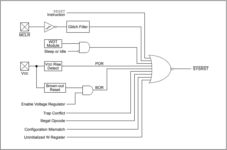
The Reset module combines all Reset sources and controls the device Master Reset Signal, \overlineSYSRST. The following is a list of device Reset sources:
- POR: Power-on Reset
- MCLR: Pin Reset
- SWR: RESET Instruction
- WDT: Watchdog Timer Reset
- BOR: Brown-out Reset
- CM: Configuration Mismatch Reset
- TRAPR: Trap Conflict Reset
- IOPUWR: Illegal Opcode Reset
- UWR: Uninitialized W Register Reset
A simplified block diagram of the Reset module is shown in Figure 6-1.
Any active source of Reset will make the \overlineSYSRST signal active. Many registers associated with the CPU and peripherals are forced to a known Reset state. Most registers are unaffected by a Reset; their status is unknown on POR and unchanged by all other Resets.
Note: Refer to the specific peripheral or CPU section of this manual for register Reset states.
All types of device Reset will set a corresponding status bit in the RCON register to indicate the type of Reset (see Register 6-1). A Power-on Reset will clear all bits except for the BOR and POR bits (RCON<1:0>) which are set. The user may set or clear any bit at any time during code execution. The RCON bits only serve as status bits. Setting a particular Reset status bit in software will not cause a device Reset to occur.
The RCON register also has other bits associated with the Watchdog Timer and device power-saving states. The function of these bits is discussed in other sections of this manual.
Note: The status bits in the RCON register should be cleared after they are read so that the next RCON register value after a device Reset will be meaningful.
FIGURE 6-1: RESET SYSTEM BLOCK DIAGRAM
REGISTER 6-1: RCON: RESET CONTROL REGISTER(1)
| R/W-0 | R/W-0 | U-0 | U-0 | U-0 | U-0 | R/W-0 | R/W-0 |
|---|---|---|---|---|---|---|---|
| TRAPR | IOPUWR | — | — | — | — | CM | PMSLP |
| bit 15 | bit 8 |
| R/W-0 | R/W-0 | R/W-0 | R/W-0 | R/W-0 | R/W-0 | R/W-1 | R/W-1 |
|---|---|---|---|---|---|---|---|
| EXTR | SWR | SWDTEN(2) | WDTO | SLEEP | IDLE | BOR | POR |
| bit 7 | bit 0 |
Legend:
R = Readable bit
W = Writable bit
U = Unimplemented bit, read as ‘0’
-n = Value at POR
‘1’ = Bit is set
‘0’ = Bit is cleared
x = Bit is unknown
bit 15
TRAPR: Trap Reset Flag bit
1 = A Trap Conflict Reset has occurred
0 = A Trap Conflict Reset has not occurred
bit 14
IOPUWR: Illegal Opcode or Uninitialized W Access Reset Flag bit
1 = An illegal opcode detection, an illegal address mode or Uninitialized W register used as an Address Pointer caused a Reset
0 = An illegal opcode or Uninitialized W register Reset has not occurred
bit 13-10
Unimplemented: Read as ‘0’
bit 9
CM: Configuration Word Mismatch Reset Flag bit
1 = A Configuration Word Mismatch Reset has occurred
0 = A Configuration Word Mismatch Reset has not occurred
bit 8
PMSLP: Program Memory Power During Sleep bit
1 = Program memory bias voltage remains powered during Sleep
0 = Program memory bias voltage is powered down during Sleep and voltage regulator enters Standby mode
bit 7
EXTR: External Reset (MCLR) Pin bit
1 = A Master Clear (pin) Reset has occurred
0 = A Master Clear (pin) Reset has not occurred
bit 6
SWR: Software Reset (Instruction) Flag bit
1 = A RESET instruction has been executed
0 = A RESET instruction has not been executed
bit 5
SWDTEN: Software Enable/Disable of WDT bit(2)
1 = WDT is enabled
0 = WDT is disabled
bit 4
WDTO: Watchdog Timer Time-out Flag bit
1 = WDT time-out has occurred
0 = WDT time-out has not occurred
bit 3
SLEEP: Wake from Sleep Flag bit
1 = Device has been in Sleep mode
0 = Device has not been in Sleep mode
Note 1: All of the Reset status bits may be set or cleared in software. Setting one of these bits in software does not cause a device Reset.
2: If the FWDEN Configuration bit is ‘1’ (unprogrammed), the WDT is always enabled, regardless of the SWDTEN bit setting.
REGISTER 6-1: RCON: RESET CONTROL REGISTER(1) (CONTINUED)
bit 2
IDLE: Wake-up from Idle Flag bit
1 = Device has been in Idle mode
0 = Device has not been in Idle mode
bit 1
BOR: Brown-out Reset Flag bit
1 = A Brown-out Reset has occurred (note that BOR is also set after a Power-on Reset)
0 = A Brown-out Reset has not occurred
bit 0
POR: Power-on Reset Flag bit
1 = A Power-on Reset has occurred
0 = A Power-on Reset has not occurred
Note 1: All of the Reset status bits may be set or cleared in software. Setting one of these bits in software does not cause a device Reset.
2: If the FWDTEN Configuration bit is ‘1’ (unprogrammed), the WDT is always enabled, regardless of the SWDTEN bit setting.
TABLE 6-1: RESET FLAG BIT OPERATION
| Flag Bit | Setting Event | Clearing Event |
|---|---|---|
| TRAPR (RCON<15>) | Trap Conflict Event | POR |
| IOPUWR (RCON<14>) | Illegal Opcode or Uninitialized W Register Access | POR |
| CM (RCON<9>) | Configuration Mismatch Reset | POR |
| EXTR (RCON<7>) | MCLR Reset | POR |
| SWR (RCON<6>) | RESET Instruction | POR |
| WDTO (RCON<4>) | WDT Time-out | PWRSAV Instruction, POR |
| SLEEP (RCON<3>) | PWRSAV #SLEEP Instruction | POR |
| IDLE (RCON<2>) | PWRSAV #IDLE Instruction | POR |
| BOR (RCON<1>) | POR, BOR | — |
| POR (RCON<0>) | POR | — |
Note: All Reset flag bits may be set or cleared by the user software.
6.1 Clock Source Selection at Reset
If clock switching is enabled, the system clock source at device Reset is chosen, as shown in Table 6-2. If clock switching is disabled, the system clock source is always selected according to the Oscillator Configuration bits. Refer to Section 8.0 “Oscillator Configuration” for further details.
TABLE 6-2: OSCILLATOR SELECTION vs. TYPE OF RESET (CLOCK SWITCHING ENABLED)
| Reset Type | Clock Source Determinant |
|---|---|
| POR | FNOSC<2:0> Configuration bits (CW2<10:8>) |
| BOR | |
| MCLR | COSC<2:0> Control bits (OSCCON<14:12>) |
| WDTO | |
| SWR |
6.2 Device Reset Times
The Reset times for various types of device Reset are summarized in Table 6-3. Note that the system Master Reset Signal, SYSRST, is released after the POR and PWRT delay times expire.
The time that the device actually begins to execute code will also depend on the system oscillator delays, which include the Oscillator Start-up Timer (OST) and the PLL lock time. The OST and PLL lock times occur in parallel with the applicable SYSRST delay times.
The FSCM delay determines the time at which the FSCM begins to monitor the system clock source after the SYSRST signal is released.
TABLE 6-3: RESET DELAY TIMES FOR VARIOUS DEVICE RESETS
| Reset Type | Clock Source | SYSRST Delay | System Clock Delay | Notes |
|---|---|---|---|---|
| POR⁽⁶⁾ | EC | TPOR + TPWRT + TRST | — | 1, 2, 7 |
| FRC, FRCDIV | TPOR + TPWRT + TRST | TFRC | 1, 2, 3, 7 | |
| LPRC | TPOR + TPWRT + TRST | TLPRC | 1, 2, 3, 7 | |
| ECPLL | TPOR + TPWRT + TRST | TLOCK | 1, 2, 4, 7 | |
| FRCPLL | TPOR + TPWRT + TRST | TFRC + TLOCK | 1, 2, 3, 4, 7 | |
| XT, HS, SOSC | TPOR + TPWRT + TRST | TOST | 1, 2, 5, 7 | |
| XTPLL, HSPLL | TPOR + TPWRT + TRST | TOST + TLOCK | 1, 2, 4, 5, 7 | |
| BOR | EC | TPWRT + TRST | — | 2, 7 |
| FRC, FRCDIV | TPWRT + TRST | TFRC | 2, 3, 7 | |
| LPRC | TPWRT + TRST | TLPRC | 2, 3, 7 | |
| ECPLL | TPWRT + TRST | TLOCK | 2, 4, 7 | |
| FRCPLL | TPWRT + TRST | TFRC + TLOCK | 2, 3, 4, 7 | |
| XT, HS, SOSC | TPWRT + TRST | TOST | 2, 5, 7 | |
| XTPLL, HSPLL | TPWRT + TRST | TFRC + TLOCK | 2, 3, 4, 7 | |
| All Others | Any Clock | TRST | — | 7 |
Note 1: TPOR = Power-on Reset delay.
2: TPWRT = 64 ms nominal if regulator is disabled (ENVREG tied to Vss).
3: TFRC and TLPRC = RC Oscillator Start-up Times.
4: TLOCK = PLL Lock Time.
5: TOST = Oscillator Start-up Timer (OST). A 10-bit counter waits 1024 oscillator periods before releasing the oscillator clock to the system.
6: If Two-Speed Start-up is enabled, regardless of the primary oscillator selected, the device starts with FRC, and in such cases, FRC start-up time is valid.
7: TRST = Internal State Reset Timer
DS39881E-page 56 © 2010-2013 Microchip Technology Inc.
6.2.1 POR AND LONG OSCILLATOR START-UP TIMES
The oscillator start-up circuitry and its associated delay timers are not linked to the device Reset delays that occur at power-up. Some crystal circuits (especially low-frequency crystals) will have a relatively long start-up time. Therefore, one or more of the following conditions is possible after SYSRST is released:
- The oscillator circuit has not begun to oscillate.
- The Oscillator Start-up Timer has not expired (if a crystal oscillator is used).
- The PLL has not achieved a lock (if PLL is used).
The device will not begin to execute code until a valid clock source has been released to the system. Therefore, the oscillator and PLL start-up delays must be considered when the Reset delay time must be known.
6.2.2 FAIL-SAFE CLOCK MONITOR (FSCM) AND DEVICE RESETS
If the FSCM is enabled, it will begin to monitor the system clock source when \overlineSYSRST is released. If a valid clock source is not available at this time, the device will automatically switch to the FRC oscillator and the user can switch to the desired crystal oscillator in the Trap Service Routine.
6.2.2.1 FSCM Delay for Crystal and PLL Clock Sources
When the system clock source is provided by a crystal oscillator and/or the PLL, a small delay, T_FSCM, will automatically be inserted after the POR and PWRT delay times. The FSCM will not begin to monitor the system clock source until this delay expires. The FSCM delay time is nominally 100 µs and provides additional time for the oscillator and/or PLL to stabilize. In most cases, the FSCM delay will prevent an oscillator failure trap at a device Reset when the PWRT is disabled.
6.3 Special Function Register Reset States
Most of the Special Function Registers (SFRs) associated with the PIC24F CPU and peripherals are reset to a particular value at a device Reset. The SFRs are grouped by their peripheral or CPU function and their Reset values are specified in each section of this manual.
The Reset value for each SFR does not depend on the type of Reset, with the exception of four registers. The Reset value for the Reset Control register, RCON, will depend on the type of device Reset. The Reset value for the Oscillator Control register, OSCCON, will depend on the type of Reset and the programmed values of the FNOSCx bits in the CW2 register (see Table 6-2). The RCFGCAL and NVMCON registers are only affected by a POR.
NOTES:
DS39881E-page 58 © 2010-2013 Microchip Technology Inc.
7.0 INTERRUPT CONTROLLER
Note: This data sheet summarizes the features of this group of PIC24F devices. It is not intended to be a comprehensive reference source. For more information, refer to the "PIC24F Family Reference Manual", "Interrupts" (DS39707).
The PIC24F interrupt controller reduces the numerous peripheral interrupt request signals to a single interrupt request signal to the PIC24F CPU. It has the following features:
- Up to 8 processor exceptions and software traps
- 7 user-selectable priority levels
- Interrupt Vector Table (IVT) with up to 118 vectors
- A unique vector for each interrupt or exception source
- Fixed priority within a specified user priority level
- Alternate Interrupt Vector Table (AIVT) for debug support
- Fixed interrupt entry and return latencies
7.1 Interrupt Vector Table
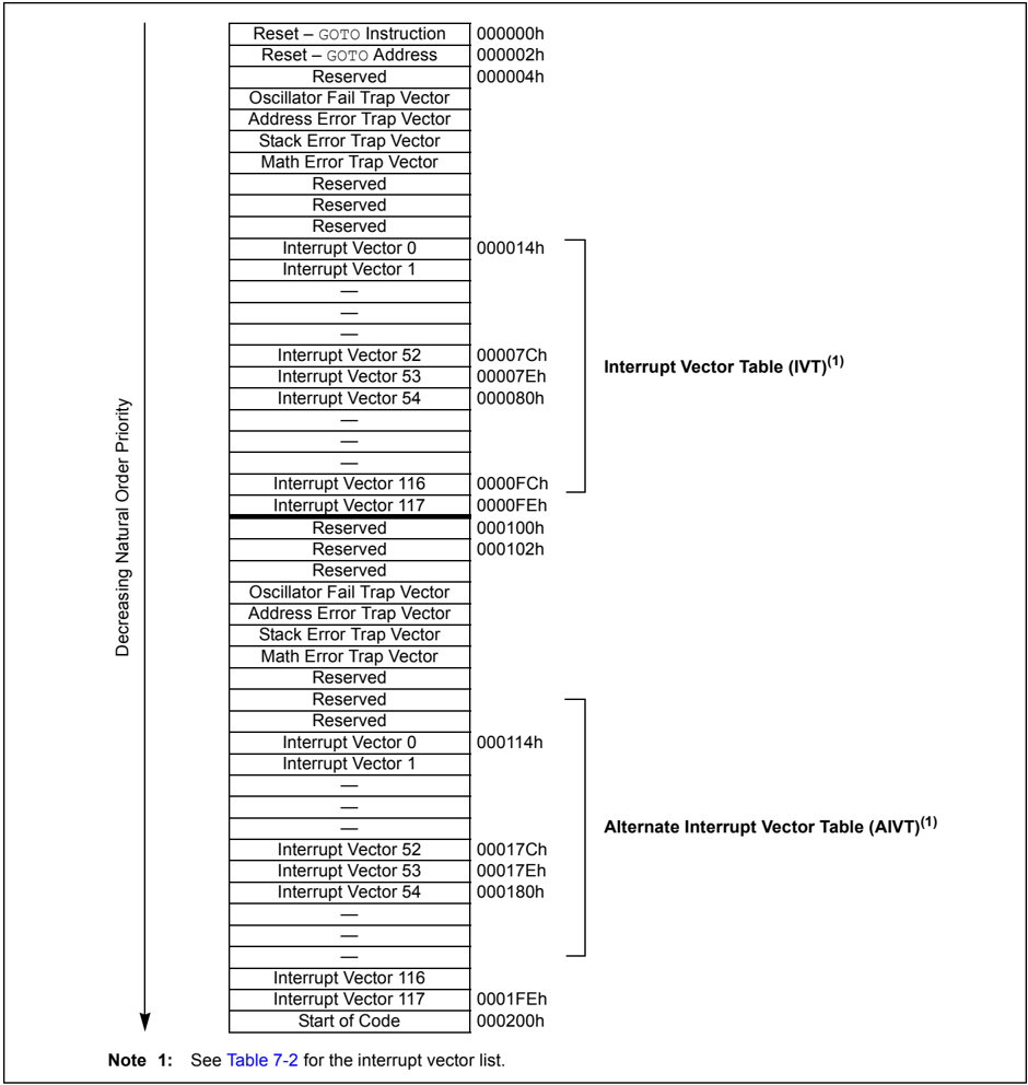
The Interrupt Vector Table (IVT) is shown in Figure 7-1. The IVT resides in program memory, starting at location, 000004h. The IVT contains 126 vectors, consisting of 8 non-maskable trap vectors, plus up to 118 sources of interrupt. In general, each interrupt source has its own vector. Each interrupt vector contains a 24-bit wide address. The value programmed into each interrupt vector location is the starting address of the associated Interrupt Service Routine (ISR).
Interrupt vectors are prioritized in terms of their natural priority; this is linked to their position in the vector table. All other things being equal, lower addresses have a higher natural priority. For example, the interrupt associated with Vector 0 will take priority over interrupts at any other vector address.
PIC24FJ64GA004 family devices implement non-maskable traps and unique interrupts. These are summarized in Table 7-1 and Table 7-2.
7.1.1 ALTERNATE INTERRUPT VECTOR TABLE
The Alternate Interrupt Vector Table (AIVT) is located after the IVT, as shown in Figure 7-1. Access to the AIVT is provided by the ALTIVT control bit (INTCON2<15>). If the ALTIVT bit is set, all interrupt and exception processes will use the alternate vectors instead of the default vectors. The alternate vectors are organized in the same manner as the default vectors.
The AIVT supports emulation and debugging efforts by providing a means to switch between an application and a support environment without requiring the interrupt vectors to be reprogrammed. This feature also enables switching between applications for evaluation of different software algorithms at run time. If the AIVT is not needed, the AIVT should be programmed with the same addresses used in the IVT.
7.2 Reset Sequence
A device Reset is not a true exception because the interrupt controller is not involved in the Reset process. The PIC24F devices clear their registers in response to a Reset which forces the PC to zero. The microcontroller then begins program execution at location, 000000h. The user programs a GOTO instruction at the Reset address, which redirects program execution to the appropriate start-up routine.
Note: Any unimplemented or unused vector locations in the IVT and AIVT should be programmed with the address of a default interrupt handler routine that contains a RESET instruction.
FIGURE 7-1: PIC24F INTERRUPT VECTOR TABLE
Note 1: See Table 7-2 for the interrupt vector list.
TABLE 7-1: TRAP VECTOR DETAILS
| Vector Number | IVT Address | AIVT Address | Trap Source |
|---|---|---|---|
| 0 | 000004h | 000104h | Reserved |
| 1 | 000006h | 000106h | Oscillator Failure |
| 2 | 000008h | 000108h | Address Error |
| 3 | 00000Ah | 00010Ah | Stack Error |
| 4 | 00000Ch | 00010Ch | Math Error |
| 5 | 00000Eh | 00010Eh | Reserved |
| 6 | 000010h | 000110h | Reserved |
| 7 | 000012h | 0001172h | Reserved |
TABLE 7-2: IMPLEMENTED INTERRUPT VECTORS
| Interrupt Source | Vector Number | IVT Address | AIVT Address | Interrupt Bit Locations | ||
|---|---|---|---|---|---|---|
| Flag | Enable | Priority | ||||
| ADC1 Conversion Done | 13 | 00002Eh | 00012Eh | IFS0<13> | IEC0<13> | IPC3<6:4> |
| Comparator Event | 18 | 000038h | 000138h | IFS1<2> | IEC1<2> | IPC4<10:8> |
| CRC Generator | 67 | 00009Ah | 00019Ah | IFS4<3> | IEC4<3> | IPC16<14:12> |
| External Interrupt 0 | 0 | 000014h | 000114h | IFS0<0> | IEC0<0> | IPC0<2:0> |
| External Interrupt 1 | 20 | 00003Ch | 00013Ch | IFS1<4> | IEC1<4> | IPC5<2:0> |
| External Interrupt 2 | 29 | 00004Eh | 00014Eh | IFS1<13> | IEC1<13> | IPC7<6:4> |
| I2C1 Master Event | 17 | 000036h | 000136h | IFS1<1> | IEC1<1> | IPC4<6:4> |
| I2C1 Slave Event | 16 | 000034h | 000034h | IFS1<0> | IEC1<0> | IPC4<2:0> |
| I2C2 Master Event | 50 | 000078h | 000178h | IFS3<2> | IEC3<2> | IPC12<10:8> |
| I2C2 Slave Event | 49 | 000076h | 000176h | IFS3<1> | IEC3<1> | IPC12<6:4> |
| Input Capture 1 | 1 | 000016h | 000116h | IFS0<1> | IEC0<1> | IPC0<6:4> |
| Input Capture 2 | 5 | 00001Eh | 00011Eh | IFS0<5> | IEC0<5> | IPC1<6:4> |
| Input Capture 3 | 37 | 00005Eh | 00015Eh | IFS2<5> | IEC2<5> | IPC9<6:4> |
| Input Capture 4 | 38 | 000060h | 000160h | IFS2<6> | IEC2<6> | IPC9<10:8> |
| Input Capture 5 | 39 | 000062h | 000162h | IFS2<7> | IEC2<7> | IPC9<14:12> |
| Input Change Notification | 19 | 00003Ah | 00013Ah | IFS1<3> | IEC1<3> | IPC4<14:12> |
| Output Compare 1 | 2 | 000018h | 000118h | IFS0<2> | IEC0<2> | IPC0<10:8> |
| Output Compare 2 | 6 | 000020h | 000120h | IFS0<6> | IEC0<6> | IPC1<10:8> |
| Output Compare 3 | 25 | 000046h | 000146h | IFS1<9> | IEC1<9> | IPC6<6:4> |
| Output Compare 4 | 26 | 000048h | 000148h | IFS1<10> | IEC1<10> | IPC6<10:8> |
| Output Compare 5 | 41 | 000066h | 000166h | IFS2<9> | IEC2<9> | IPC10<6:4> |
| Parallel Master Port | 45 | 00006Eh | 00016Eh | IFS2<13> | IEC2<13> | IPC11<6:4> |
| Real-Time Clock/Calendar | 62 | 000090h | 000190h | IFS3<14> | IEC3<14> | IPC15<10:8> |
| SPI1 Error | 9 | 000026h | 000126h | IFS0<9> | IEC0<9> | IPC2<6:4> |
| SPI1 Event | 10 | 000028h | 000128h | IFS0<10> | IEC0<10> | IPC2<10:8> |
| SPI2 Error | 32 | 000054h | 000154h | IFS2<0> | IEC0<0> | IPC8<2:0> |
| SPI2 Event | 33 | 000056h | 000156h | IFS2<1> | IEC2<1> | IPC8<6:4> |
| Timer1 | 3 | 00001Ah | 00011Ah | IFS0<3> | IEC0<3> | IPC0<14:12> |
| Timer2 | 7 | 000022h | 000122h | IFS0<7> | IEC0<7> | IPC1<14:12> |
| Timer3 | 8 | 000024h | 000124h | IFS0<8> | IEC0<8> | IPC2<2:0> |
| Timer4 | 27 | 00004Ah | 00014Ah | IFS1<11> | IEC1<11> | IPC6<14:12> |
| Timer5 | 28 | 00004Ch | 00014Ch | IFS1<12> | IEC1<12> | IPC7<2:0> |
| UART1 Error | 65 | 000096h | 000196h | IFS4<1> | IEC4<1> | IPC16<6:4> |
| UART1 Receiver | 11 | 00002Ah | 00012Ah | IFS0<11> | IEC0<11> | IPC2<14:12> |
| UART1 Transmitter | 12 | 00002Ch | 00012Ch | IFS0<12> | IEC0<12> | IPC3<2:0> |
| UART2 Error | 66 | 000098h | 000198h | IFS4<2> | IEC4<2> | IPC16<10:8> |
| UART2 Receiver | 30 | 000050h | 000150h | IFS1<14> | IEC1<14> | IPC7<10:8> |
| UART2 Transmitter | 31 | 000052h | 000152h | IFS1<15> | IEC1<15> | IPC7<14:12> |
| Low-Voltage Detect (LVD) | 72 | 0000A4h | 000124h | IFS4<8> | IEC4<8> | IPC17<2:0> |
7.3 Interrupt Control and Status Registers
The PIC24FJ64GA004 family of devices implements a total of 29 registers for the interrupt controller:
- INTCON1
- INTCON2
- IFS0 through IFS4
- IEC0 through IEC4
- IPC0 through IPC12, IPC15, IPC16 and IPC18
- INTTREG
Global interrupt control functions are controlled from INTCON1 and INTCON2. INTCON1 contains the Interrupt Nesting Disable (NSTDIS) bit, as well as the control and status flags for the processor trap sources. The INTCON2 register controls the external interrupt request signal behavior and the use of the Alternate Interrupt Vector Table.
The IFSx registers maintain all of the interrupt request flags. Each source of interrupt has a status bit which is set by the respective peripherals, or external signal, and is cleared via software.
The IECx registers maintain all of the interrupt enable bits. These control bits are used to individually enable interrupts from the peripherals or external signals.
The IPCx registers are used to set the Interrupt Priority Level (IPL) for each source of interrupt. Each user interrupt source can be assigned to one of eight priority levels.
The INTTREG register contains the associated interrupt vector number and the new CPU Interrupt Priority Level, which are latched into the Vector Number (VECNUM<6:0>) and the Interrupt Level (ILR<3:0>) bit fields in the INTTREG register. The new Interrupt Priority Level is the priority of the pending interrupt.
The interrupt sources are assigned to the IFSx, IECx and IPCx registers in the same sequence that they are listed in Table 7-2. For example, the INT0 (External Interrupt 0) is shown as having a vector number and a natural order priority of 0. Thus, the INT0IF status bit is found in IFS0<0>, the INT0IE enable bit in IEC0<0> and the INT0IP<2:0> priority bits in the first position of IPC0 (IPC0<2:0>).
Although they are not specifically part of the interrupt control hardware, two of the CPU control registers contain bits that control interrupt functionality. The ALU STATUS Register (SR) contains the IPL<2:0> bits (SR<7:5>). These indicate the current CPU Interrupt Priority Level. The user may change the current CPU priority level by writing to the IPLx bits.
The CORCON register contains the IPL3 bit, which together with IPL<2:0>, also indicates the current CPU priority level. IPL3 is a read-only bit so that trap events cannot be masked by the user software.
All Interrupt registers are described in Register 7-1 through Register 7-31, in the following pages.
REGISTER 7-1: SR: ALU STATUS REGISTER (IN CPU)
| U-0 | U-0 | U-0 | U-0 | U-0 | U-0 | U-0 | R/W-0 |
|---|---|---|---|---|---|---|---|
| — | — | — | — | — | — | — | DC(1) |
| bit 15 | bit 8 |
| R/W-0 | R/W-0 | R/W-0 | R-0 | R/W-0 | R/W-0 | R/W-0 | R/W-0 |
|---|---|---|---|---|---|---|---|
| IPL2(2,3) | IPL1(2,3) | IPL0(2,3) | RA(1) | N(1) | OV(1) | Z(1) | C(1) |
| bit 7 | bit 0 |
Legend:
R = Readable bit
W = Writable bit
U = Unimplemented bit, read as ‘0’
-n = Value at POR
‘1’ = Bit is set
‘0’ = Bit is cleared
x = Bit is unknown
bit 7-5 IPL<2:0>: CPU Interrupt Priority Level Status bits(2,3)
111 = CPU Interrupt Priority Level is 7 (15); user interrupts are disabled
110 = CPU Interrupt Priority Level is 6 (14)
101 = CPU Interrupt Priority Level is 5 (13)
100 = CPU Interrupt Priority Level is 4 (12)
011 = CPU Interrupt Priority Level is 3 (11)
010 = CPU Interrupt Priority Level is 2 (10)
001 = CPU Interrupt Priority Level is 1 (9)
000 = CPU Interrupt Priority Level is 0 (8)
Note 1:
See Register 3-1 for the description of the remaining bit(s) that are not dedicated to interrupt control functions.
Note 2:
The IPLx bits are concatenated with the IPL3 bit (CORCON<3>) to form the CPU interrupt Priority Level.
The value in parentheses indicates the Interrupt Priority Level if IPL3 = 1.
Note 3:
The IPLx Status bits are read-only when NSTDIS (INTCON1<15>) = 1.
REGISTER 7-2: CORCON: CPU CONTROL REGISTER
| U-0 | U-0 | U-0 | U-0 | U-0 | U-0 | U-0 | U-0 |
|---|---|---|---|---|---|---|---|
| — | — | — | — | — | — | — | — |
| bit 15 | bit 8 |
| U-0 | U-0 | U-0 | U-0 | R/C-0 | R/W-0 | U-0 | U-0 |
|---|---|---|---|---|---|---|---|
| — | — | — | — | IPL3(2) | PSV(1) | — | — |
| bit 7 | bit 0 |
Legend:
C = Clearable bit
R = Readable bit
W = Writable bit
U = Unimplemented bit, read as ‘0’
-n = Value at POR
‘1’ = Bit is set
‘0’ = Bit is cleared
x = Bit is unknown
bit 3 IPL3: CPU Interrupt Priority Level Status bit(2)
1 = CPU Interrupt Priority Level is greater than 7
0 = CPU Interrupt Priority Level is 7 or less
Note 1:
See Register 3-2 for the description of the remaining bit(s) that are not dedicated to interrupt control functions.
Note 2:
The IPL3 bit is concatenated with the IPL<2:0: bits (SR<7:5>) to form the CPU Interrupt priority Level.
REGISTER 7-3: INTCON1: INTERRUPT CONTROL REGISTER 1
| R/W-0 | U-0 | U-0 | U-0 | U-0 | U-0 | U-0 | U-0 |
|---|---|---|---|---|---|---|---|
| NSTDIS | — | — | — | — | — | — | — |
| bit 15 | bit 8 |
| U-0 | U-0 | U-0 | R/W-0 | R/W-0 | R/W-0 | R/W-0 | U-0 |
|---|---|---|---|---|---|---|---|
| — | — | — | MATHERR | ADDRERR | STKERR | OSCFAIL | — |
| bit 7 | bit 0 |
Legend:
R = Readable bit
W = Writable bit
U = Unimplemented bit, read as ‘0’
-n = Value at POR
‘1’ = Bit is set
‘0’ = Bit is cleared
x = Bit is unknown
bit 15
NSTDIS: Interrupt Nesting Disable bit
1 = Interrupt nesting is disabled
0 = Interrupt nesting is enabled
bit 14-5
Unimplemented: Read as ‘0’
bit 4
MATHERR: Arithmetic Error Trap Status bit
1 = Overflow trap has occurred
0 = Overflow trap has not occurred
bit 3
ADDRERR: Address Error Trap Status bit
1 = Address error trap has occurred
0 = Address error trap has not occurred
bit 2
STKERR: Stack Error Trap Status bit
1 = Stack error trap has occurred
0 = Stack error trap has not occurred
bit 1
OSCFAIL: Oscillator Failure Trap Status bit
1 = Oscillator failure trap has occurred
0 = Oscillator failure trap has not occurred
bit 0
Unimplemented: Read as ‘0’
REGISTER 7-4: INTCON2: INTERRUPT CONTROL REGISTER 2
| R/W-0 | R-0 | U-0 | U-0 | U-0 | U-0 | U-0 | U-0 |
|---|---|---|---|---|---|---|---|
| ALTIVT | DISI | — | — | — | — | — | — |
| bit 15 | bit 8 |
| U-0 | U-0 | U-0 | U-0 | U-0 | R/W-0 | R/W-0 | R/W-0 |
|---|---|---|---|---|---|---|---|
| — | — | — | — | — | INT2EP | INT1EP | INT0EP |
| bit 7 | bit 0 |
Legend:
R = Readable bit
W = Writable bit
U = Unimplemented bit, read as ‘0’
-n = Value at POR
‘1’ = Bit is set
‘0’ = Bit is cleared
x = Bit is unknown
bit 15
ALTIVT: Enable Alternate Interrupt Vector Table bit
1 = Uses Alternate Interrupt Vector Table
0 = Uses standard (default) Interrupt Vector Table
bit 14
DISI: DISI Instruction Status bit
1 = DISI instruction is active
0 = DISI instruction is not active
bit 13-3
Unimplemented: Read as ‘0’
bit 2
INT2EP: External Interrupt 2 Edge Detect Polarity Select bit
1 = Interrupt on negative edge
0 = Interrupt on positive edge
bit 1
INT1EP: External Interrupt 1 Edge Detect Polarity Select bit
1 = Interrupt on negative edge
0 = Interrupt on positive edge
bit 0
INT0EP: External Interrupt 0 Edge Detect Polarity Select bit
1 = Interrupt on negative edge
0 = Interrupt on positive edge
REGISTER 7-5: IFS0: INTERRUPT FLAG STATUS REGISTER 0
| U-0 | U-0 | R/W-0 | R/W-0 | R/W-0 | R/W-0 | R/W-0 | R/W-0 |
|---|---|---|---|---|---|---|---|
| — | — | AD1IF | U1TXIF | U1RXIF | SPI1IF | SPF1IF | T3IF |
| bit 15 | bit 8 |
| R/W-0 | R/W-0 | R/W-0 | U-0 | R/W-0 | R/W-0 | R/W-0 | R/W-0 |
|---|---|---|---|---|---|---|---|
| T2IF | OC2IF | IC2IF | — | T1IF | OC1IF | IC1IF | INT0IF |
| bit 7 | bit 0 |
Legend:
R = Readable bit
W = Writable bit
U = Unimplemented bit, read as ‘0’
-n = Value at POR
‘1’ = Bit is set
‘0’ = Bit is cleared
x = Bit is unknown
bit 15-14 Unimplemented: Read as ‘0’
bit 13 AD1IF: A/D Conversion Complete Interrupt Flag Status bit
1 = Interrupt request has occurred
0 = Interrupt request has not occurred
bit 12 U1TXIF: UART1 Transmitter Interrupt Flag Status bit
1 = Interrupt request has occurred
0 = Interrupt request has not occurred
bit 11 U1RXIF: UART1 Receiver Interrupt Flag Status bit
1 = Interrupt request has occurred
0 = Interrupt request has not occurred
bit 10 SPI1IF: SPI1 Event Interrupt Flag Status bit
1 = Interrupt request has occurred
0 = Interrupt request has not occurred
bit 9 SPF1IF: SPI1 Fault Interrupt Flag Status bit
1 = Interrupt request has occurred
0 = Interrupt request has not occurred
bit 8 T3IF: Timer3 Interrupt Flag Status bit
1 = Interrupt request has occurred
0 = Interrupt request has not occurred
bit 7 T2IF: Timer2 Interrupt Flag Status bit
1 = Interrupt request has occurred
0 = Interrupt request has not occurred
bit 6 OC2IF: Output Compare Channel 2 Interrupt Flag Status bit
1 = Interrupt request has occurred
0 = Interrupt request has not occurred
bit 5 IC2IF: Input Capture Channel 2 Interrupt Flag Status bit
1 = Interrupt request has occurred
0 = Interrupt request has not occurred
bit 4 Unimplemented: Read as ‘0’
bit 3 T1IF: Timer1 Interrupt Flag Status bit
1 = Interrupt request has occurred
0 = Interrupt request has not occurred
bit 2 OC1IF: Output Compare Channel 1 Interrupt Flag Status bit
1 = Interrupt request has occurred
0 = Interrupt request has not occurred
REGISTER 7-5: IFS0: INTERRUPT FLAG STATUS REGISTER 0 (CONTINUED)
bit 1 IC1IF: Input Capture Channel 1 Interrupt Flag Status bit 1 = Interrupt request has occurred 0 = Interrupt request has not occurred
bit 0 INT0IF: External Interrupt 0 Flag Status bit 1 = Interrupt request has occurred 0 = Interrupt request has not occurred
REGISTER 7-6: IFS1: INTERRUPT FLAG STATUS REGISTER 1
| R/W-0 | R/W-0 | R/W-0 | R/W-0 | R/W-0 | R/W-0 | R/W-0 | U-0 |
|---|---|---|---|---|---|---|---|
| U2TXIF | U2RXIF | INT2IF | T5IF | T4IF | OC4IF | OC3IF | — |
| bit 15 | bit 8 |
| U-0 | U-0 | U-0 | R/W-0 | R/W-0 | R/W-0 | R/W-0 | R/W-0 |
|---|---|---|---|---|---|---|---|
| — | — | — | INT1IF | CNIF | CMIF | MI2C1IF | SI2C1IF |
| bit 7 | bit 0 |
Legend:
R = Readable bit
W = Writable bit
U = Unimplemented bit, read as ‘0’
-n = Value at POR
‘1’ = Bit is set
‘0’ = Bit is cleared
x = Bit is unknown
bit 15 U2TXIF: UART2 Transmitter Interrupt Flag Status bit
1 = Interrupt request has occurred
0 = Interrupt request has not occurred
bit 14 U2RXIF: UART2 Receiver Interrupt Flag Status bit
1 = Interrupt request has occurred
0 = Interrupt request has not occurred
bit 13 INT2IF: External Interrupt 2 Flag Status bit
1 = Interrupt request has occurred
0 = Interrupt request has not occurred
bit 12 T5IF: Timer5 Interrupt Flag Status bit
1 = Interrupt request has occurred
0 = Interrupt request has not occurred
bit 11 T4IF: Timer4 Interrupt Flag Status bit
1 = Interrupt request has occurred
0 = Interrupt request has not occurred
bit 10 OC4IF: Output Compare Channel 4 Interrupt Flag Status bit
1 = Interrupt request has occurred
0 = Interrupt request has not occurred
bit 9 OC3IF: Output Compare Channel 3 Interrupt Flag Status bit
1 = Interrupt request has occurred
0 = Interrupt request has not occurred
bit 8-5 Unimplemented: Read as ‘0’
bit 4 INT1IF: External Interrupt 1 Flag Status bit
1 = Interrupt request has occurred
0 = Interrupt request has not occurred
bit 3 CNIF: Input Change Notification Interrupt Flag Status bit
1 = Interrupt request has occurred
0 = Interrupt request has not occurred
bit 2 CMIF: Comparator Interrupt Flag Status bit
1 = Interrupt request has occurred
0 = Interrupt request has not occurred
bit 1 MI2C1IF: Master I2C1 Event Interrupt Flag Status bit
1 = Interrupt request has occurred
0 = Interrupt request has not occurred
bit 0 SI2C1IF: Slave I2C1 Event Interrupt Flag Status bit
1 = Interrupt request has occurred
0 = Interrupt request has not occurred
REGISTER 7-7: IFS2: INTERRUPT FLAG STATUS REGISTER 2
| U-0 | U-0 | R/W-0 | U-0 | U-0 | U-0 | R/W-0 | U-0 |
|---|---|---|---|---|---|---|---|
| — | — | PMPIF | — | — | — | OC5IF | — |
| bit 15 | bit 8 |
| R/W-0 | R/W-0 | R/W-0 | U-0 | U-0 | U-0 | R/W-0 | R/W-0 |
|---|---|---|---|---|---|---|---|
| IC5IF | IC4IF | IC3IF | — | — | — | SPI2IF | SPF2IF |
| bit 7 | bit 0 |
Legend:
R = Readable bit
W = Writable bit
U = Unimplemented bit, read as ‘0’
-n = Value at POR
‘1’ = Bit is set
‘0’ = Bit is cleared
x = Bit is unknown
bit 15-14 Unimplemented: Read as ‘0’
bit 13 PMPIF: Parallel Master Port Interrupt Flag Status bit
1 = Interrupt request has occurred
0 = Interrupt request has not occurred
bit 12-10 Unimplemented: Read as ‘0’
bit 9 OC5IF: Output Compare Channel 5 Interrupt Flag Status bit
1 = Interrupt request has occurred
0 = Interrupt request has not occurred
bit 8 Unimplemented: Read as ‘0’
bit 7 IC5IF: Input Capture Channel 5 Interrupt Flag Status bit
1 = Interrupt request has occurred
0 = Interrupt request has not occurred
bit 6 IC4IF: Input Capture Channel 4 Interrupt Flag Status bit
1 = Interrupt request has occurred
0 = Interrupt request has not occurred
bit 5 IC3IF: Input Capture Channel 3 Interrupt Flag Status bit
1 = Interrupt request has occurred
0 = Interrupt request has not occurred
bit 4-2 Unimplemented: Read as ‘0’
bit 1 SPI2IF: SPI2 Event Interrupt Flag Status bit
1 = Interrupt request has occurred
0 = Interrupt request has not occurred
bit 0 SPF2IF: SPI2 Fault Interrupt Flag Status bit
1 = Interrupt request has occurred
0 = Interrupt request has not occurred
REGISTER 7-8: IFS3: INTERRUPT FLAG STATUS REGISTER 3
| U-0 | R/W-0 | U-0 | U-0 | U-0 | U-0 | U-0 | U-0 |
|---|---|---|---|---|---|---|---|
| — | RTCIF | — | — | — | — | — | — |
| bit 15 | bit 8 |
| U-0 | U-0 | U-0 | U-0 | U-0 | R/W-0 | R/W-0 | U-0 |
|---|---|---|---|---|---|---|---|
| — | — | — | — | — | MI2C2IF | SI2C2IF | — |
| bit 7 | bit 0 |
Legend:
R = Readable bit
W = Writable bit
U = Unimplemented bit, read as ‘0’
-n = Value at POR
‘1’ = Bit is set
‘0’ = Bit is cleared
x = Bit is unknown
bit 15 Unimplemented: Read as ‘0’
bit 14 RTCIF: Real-Time Clock/Calendar Interrupt Flag Status bit
1 = Interrupt request has occurred
0 = Interrupt request has not occurred
bit 13-3 Unimplemented: Read as ‘0’
bit 2 MI2C2IF: Master I2C2 Event Interrupt Flag Status bit
1 = Interrupt request has occurred
0 = Interrupt request has not occurred
bit 1 SI2C2IF: Slave I2C2 Event Interrupt Flag Status bit
1 = Interrupt request has occurred
0 = Interrupt request has not occurred
bit 0 Unimplemented: Read as ‘0’
REGISTER 7-9: IFS4: INTERRUPT FLAG STATUS REGISTER 4
| U-0 | U-0 | U-0 | U-0 | U-0 | U-0 | U-0 | R/W-0 |
|---|---|---|---|---|---|---|---|
| — | — | — | — | — | — | — | LVDIF |
| bit 15 | bit 8 |
| U-0 | U-0 | U-0 | U-0 | R/W-0 | R/W-0 | R/W-0 | U-0 |
|---|---|---|---|---|---|---|---|
| — | — | — | — | CRCIF | U2ERIF | U1ERIF | — |
| bit 7 | bit 0 |
Legend:
R = Readable bit
W = Writable bit
U = Unimplemented bit, read as ‘0’
-n = Value at POR
‘1’ = Bit is set
‘0’ = Bit is cleared
x = Bit is unknown
bit 15-9 Unimplemented: Read as ‘0’
bit 8 LVDIF: Low-Voltage Detect Interrupt Flag Status bit
1 = Interrupt request has occurred
0 = Interrupt request has not occurred
bit 7-4 Unimplemented: Read as ‘0’
bit 3 CRCIF: CRC Generator Interrupt Flag Status bit
1 = Interrupt request has occurred
0 = Interrupt request has not occurred
bit 2 U2ERIF: UART2 Error Interrupt Flag Status bit
1 = Interrupt request has occurred
0 = Interrupt request has not occurred
bit 1 U1ERIF: UART1 Error Interrupt Flag Status bit
1 = Interrupt request has occurred
0 = Interrupt request has not occurred
bit 0 Unimplemented: Read as ‘0’