8.12.5.15 On-Chip Analog-to-Digital Converter
8.12.5.15.1 ADC Absolute Maximum Ratings Over Recommended Operating Conditions (Unless Otherwise Noted)
| MIN(1) | MAX | UNIT | ||
|---|---|---|---|---|
| Supply voltage range | VSSA1/VSSA2 to VDDA1/VDDA2/AVDDREFBG | –0.3 | 4.6 | V |
| Supply voltage range | VSS1 to VDD1 | –0.3 | 2.5 | V |
| Analog Input (ADCIN) Clamp Current, total (max) | –20(2) | 20(2) | mA |
(1) Unless otherwise noted, the list of absolute maximum ratings are specified over recommended operating conditions. Stresses beyond those listed under Absolute Maximum Ratings may cause permanent damage to the device. These are stress ratings only, and functional operation of the device at these or any other conditions beyond those indicated under Recommended Operating Conditions is not implied. Exposure to absolute-maximum-rated conditions for extended periods may affect device reliability.
(2) The analog inputs have an internal clamping circuit that clamps the voltage to a diode drop above VDDA or below VSS. The continuous clamp current per pin is ±2 mA.
8.12.5.15.2 ADC Electrical Characteristics Over Recommended Operating Conditions (Unless Otherwise Noted)—AC Specifications
| PARAMETER | MIN | TYP | MAX | UNIT | |
|---|---|---|---|---|---|
| SINAD | Signal-to-noise ratio + distortion | 62 | dB | ||
| SNR | Signal-to-noise ratio | 62 | dB | ||
| THD (100 kHz) | Total harmonic distortion | –68 | dB | ||
| ENOB (SNR) | Effective number of bits | 10.1 | Bits | ||
| SFDR | Spurious free dynamic range | 69 | dB |

8.12.5.15.3 ADC Electrical Characteristics Over Recommended Operating Conditions (Unless Otherwise Noted)—DC Specifications
| PARAMETER(1) | MIN | TYP | MAX | UNIT |
|---|---|---|---|---|
| Resolution | 12 | Bits | ||
| ADC clock(2) | 1 | kHz | ||
| 25 | MHz | |||
| ACCURACY | ||||
| INL (Integral nonlinearity)(3) | 1–18.75 MHz ADC clock | ±1.5 | LSB | |
| DNL (Differential nonlinearity)(3) | 1–18.75 MHz ADC clock | ±1 | LSB | |
| Offset error(4) | –80 | 80 | LSB | |
| Overall gain error with internal reference(5) | –200 | 200 | LSB | |
| Overall gain error with external reference(6) | If ADCREFP – ADCREFM = 1 V ± 0.1% | –50 | 50 | LSB |
| Channel-to-channel offset variation | ±8 | LSB | ||
| Channel-to-channel Gain variation | ±8 | LSB | ||
| ANALOG INPUT | ||||
| Analog input voltage (ADCINx to ADCLO)(7) | 0 | 3 | V | |
| ADCLO | –5 | 0 | 5 mV | |
| Input capacitance | 10 | pF | ||
| Input leakage current | 3 | ±5 μA | ||
| INTERNAL VOLTAGE REFERENCE (5) | ||||
| Accuracy, ADCVREFP | 1.9 | 2 | 2.1 V | |
| Accuracy, ADCVREFM | 0.95 | 1 | 1.05 V | |
| Voltage difference, ADCREFP – ADCREFM | 1 | V | ||
| Temperature coefficient | 50 | PPM/°C | ||
| Reference noise | 100 | μV | ||
| EXTERNAL VOLTAGE REFERENCE (6) | ||||
| Accuracy, ADCVREFP | 1.9 | 2 | 2.1 V | |
| Accuracy, ADCVREFM | 0.95 | 1 | 1.05 V | |
| Input voltage difference, ADCREFP – ADCREFM | 0.99 | 1 | 1.01 V |
(1) Tested at 12.5-MHz ADCCLK.
(2) If SYSCLKOUT ≤ 25 MHz, ADC clock ≤ SYSCLKOUT/2.
(3) The INL degrades for frequencies beyond 18.75 MHz–25 MHz. Applications that require these sampling rates should use a 20K resistor as bias resistor on the ADCRESEXT pin. This improves overall linearity and typical current drawn by the ADC will be a few mA more than 24.9-kΩ bias.
(4) 1 LSB has the weighted value of 3.0/4096 = 0.732 mV.
(5) A single internal band gap reference (±5% accuracy) sources both ADCREFP and ADCREFM signals, and hence, these voltages track together. The ADC converter uses the difference between these two as its reference. The total gain error will be the combination of the gain error shown here and the voltage reference accuracy (ADCREFP – ADCREFM). A software-based calibration procedure is recommended for better accuracy. See the F2810, F2811, and F2812 ADC Calibration Application Report and Section 11.4 for relevant documents.
(6) In this mode, the accuracy of external reference is critical for overall gain. The voltage difference (ADCREFP – ADCREFM) will determine the overall accuracy.
(7) Voltages above VDDA + 0.3 V or below VSS – 0.3 V applied to an analog input pin may temporarily affect the conversion of another pin. To avoid this, the analog inputs should be kept within these limits.
8.12.5.15.4 Current Consumption for Different ADC Configurations
8.12.5.15.4.1 Current Consumption for Different ADC Configurations (at 25-MHz ADCCLK)
| IDDA (TYP)(1)(2) | IDDAIO (TYP) | IDD1 (TYP) | ADC OPERATING MODE/CONDITIONS |
|---|---|---|---|
| 40 mA | 1 µA | 0.5 mA | Mode A (Operational Mode):• BG and REF enabled• PWD disabled |
| 7 mA | 0 | 5 µA | Mode B:• ADC clock enabled• BG and REF enabled• PWD enabled |
| 1 µA | 0 | 5 µA | Mode C:• ADC clock enabled• BG and REF disabled• PWD enabled |
| 1 µA | 0 | 0 | Mode D:• ADC clock disabled• BG and REF disabled• PWD enabled |
(1) Test Conditions:
- SYSCLKOUT = 150 MHz
- ADC module clock = 25 MHz
- ADC performing a continuous conversion of all 16 channels in Mode A
(2) IDDA – includes current into VDDA1/VDDA2 and AVDDREFBG
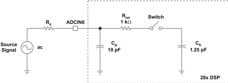
Typical Values of the Input Circuit Components:
- Switch Resistance (Ron): 1 kΩ
- Sampling Capacitor (Ch): 1.25 pF
- Parasitic Capacitance (Cp): 10 pF
- Source Resistance (Rs): 50 Ω
Figure 8-35. ADC Analog Input Impedance Model

8.12.5.15.5 ADC Power-Up Control Bit Timing
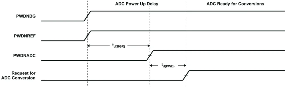
Figure 8-36. ADC Power-Up Control Bit Timing
8.12.5.15.5.1 ADC Power-Up Delays
| MIN(1) | TYP | MAX | UNIT | ||
|---|---|---|---|---|---|
| td(BGR) | Delay time for band gap reference to be stable. Bits 7 and 6 of the ADCTRL3 register (ADCBGRFDN1/0) are to be set to 1 before the ADCPWDN bit is enabled. | 7 | 8 | 10 | ms |
| td(PWD) | Delay time for power-down control to be stable. Bit 5 of the ADCTRL3 register (ADCPWDN) is to be set to 1 before any ADC conversions are initiated. | 20 | 50 | μs | |
| 1 | ms |
(1) These delays are necessary and recommended to make the ADC analog reference circuit stable before conversions are initiated. If conversions are started without these delays, the ADC results will show a higher gain. For power down, all three bits can be cleared at the same time.
8.12.5.15.6 Detailed Description
8.12.5.15.6.1 Reference Voltage
The on-chip ADC has a built-in reference, which provides the reference voltages for the ADC. ADCVREFP is set to 2.0 V and ADCVREFM is set to 1.0 V.
8.12.5.15.6.2 Analog Inputs
The on-chip ADC consists of 16 analog inputs, which are sampled either one at a time or two channels at a time. These inputs are software-selectable.
8.12.5.15.6.3 Converter
The on-chip ADC uses a 12-bit four-stage pipeline architecture, which achieves a high sample rate with low power consumption.
8.12.5.15.6.4 Conversion Modes
The conversion can be performed in two different conversion modes:
- Sequential sampling mode (SMODE = 0)
- Simultaneous sampling mode (SMODE = 1)
TMS320F2810, TMS320F2810-Q1, TMS320F2811, TMS320F2811-Q1
8.12.5.15.7 Sequential Sampling Mode (Single-Channel) (SMODE = 0)
In sequential sampling mode, the ADC can continuously convert input signals on any of the channels (Ax to Bx). The ADC can start conversions on event triggers from the Event Managers (EVA/EVB), software trigger, or from an external ADCSOC signal. If the SMODE bit is 0, the ADC will do conversions on the selected channel on every Sample/Hold pulse. The conversion time and latency of the Result register update are explained below. The ADC interrupt flags are set a few SYSCLKOUT cycles after the Result register update. The selected channels will be sampled at every falling edge of the Sample/Hold pulse. The Sample/Hold pulse width can be programmed to be 1 ADC clock wide (minimum) or 16 ADC clocks wide (maximum).
 Figure 8-37. Sequential Sampling Mode (Single-Channel) Timing
8.12.5.15.7.1 Sequential Sampling Mode Timing

TEXAS INSTRUMENTS www.ti.com
8.12.5.15.8 Simultaneous Sampling Mode (Dual-Channel) (SMODE = 1)
In simultaneous mode, the ADC can continuously convert input signals on any one pair of channels (A0/B0 to A7/B7). The ADC can start conversions on event triggers from the Event Managers (EVA/EVB), software trigger, or from an external ADCSOC signal. If the SMODE bit is 1, the ADC will do conversions on two selected channels on every Sample/Hold pulse. The conversion time and latency of the Result register update are explained below. The ADC interrupt flags are set a few SYSCLKOUT cycles after the Result register update. The selected channels will be sampled simultaneously at the falling edge of the Sample/Hold pulse. The Sample/Hold pulse width can be programmed to be 1 ADC clock wide (minimum) or 16 ADC clocks wide (maximum).
Note
In Simultaneous Mode, the ADCIN channel pair select has to be A0/B0, A1/B1, ..., A7/B7, and not in other combinations (such as A1/B3, and so forth).
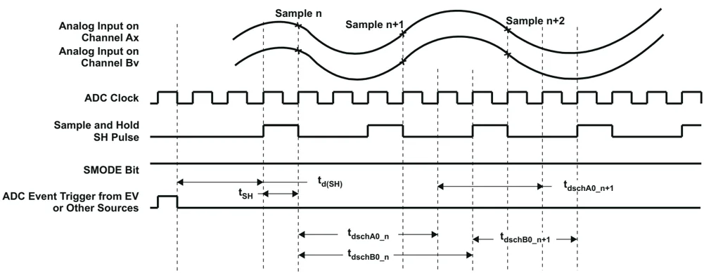
Figure 8-38. Simultaneous Sampling Mode Timing
8.12.5.15.8.1 Simultaneous Sampling Mode Timing
TMS320F2810, TMS320F2810-Q1, TMS320F2811, TMS320F2811-Q1 TMS320F2812, TMS320F2812-Q1
www.ti.com SPRS174V – APRIL 2001 – REVISED FEBRUARY 2021
8.12.5.15.9 Definitions of Specifications and Terminology
I ntegral Nonlinearity
Integral nonlinearity refers to the deviation of each individual code from a line drawn from zero through full scale. The point used as zero occurs 1/2 LSB before the first code transition. The full-scale point is defined as level 1/2 LSB beyond the last code transition. The deviation is measured from the center of each particular code to the true straight line between these two points.
Differential Nonlinearity
An ideal ADC exhibits code transitions that are exactly 1 LSB apart. DNL is the deviation from this ideal value. A differential nonlinearity error of less than ±1 LSB ensures no missing codes.
Zero Offset
The major carry transition should occur when the analog input is at zero volt. Zero error is defined as the deviation of the actual transition from that point.
Gain Error
The first code transition should occur at an analog value 1/2 LSB above negative full scale. The last transition should occur at an analog value 1 1/2 LSB below the nominal full scale. Gain error is the deviation of the actual difference between first and last code transitions and the ideal difference between first and last code transitions.
Signal-to-Noise Ratio + Distortion (SINAD)
SINAD is the ratio of the rms value of the measured input signal to the rms sum of all other spectral components below the Nyquist frequency, including harmonics but excluding dc. The value for SINAD is expressed in decibels.
Effective Number of Bits (ENOB)
For a sine wave, SINAD can be expressed in terms of the number of bits. Using the following formula,
$$ N = \frac{(\text{SINAD} - 1.76)}{6.02} $$
it is possible to get a measure of performance expressed as N, the effective number of bits. Thus, effective number of bits for a device for sine wave inputs at a given input frequency can be calculated directly from its measured SINAD.
Total Harmonic Distortion (THD)
THD is the ratio of the rms sum of the first six harmonic components to the rms value of the measured input signal and is expressed as a percentage or in decibels.
Spurious Free Dynamic Range (SFDR)
SFDR is the difference in dB between the rms amplitude of the input signal and the peak spurious signal.
Copyright © 2021 Texas Instruments Incorporated Submit Document Feedback 75

8.12.5.16 Multichannel Buffered Serial Port (McBSP) Timing
8.12.5.16.1 McBSP Transmit and Receive Timing
8.12.5.16.1.1 McBSP Timing Requirements
(1) Polarity bits CLKRP = CLKXP = FSRP = FSXP = 0. If the polarity of any of the signals is inverted, then the timing references of that signal are also inverted.
(2) 2P = 1/CLKG in ns. CLKG is the output of sample rate generator mux. CLKG = CLKSRG/(1 + CLKGDV). CLKSRG can be LSPCLK, CLKX, CLKR as source. CLKSRG ≤ (SYSCLKOUT/2). McBSP performance is limited by I/O buffer switching speed.
(3) Internal clock prescalers must be adjusted such that the McBSP clock (CLKG, CLKX, CLKR) speeds are not greater than the I/O buffer speed limit (20 MHz).
TMS320F2810, TMS320F2810-Q1, TMS320F2811, TMS320F2811-Q1
8.12.5.16.1.2 McBSP Switching Characteristics
\begin{tabular}{|l|l|p{5.5cm}|l|r|r|l|} \hline \textbf{NO.\textsuperscript{(1)}(2)} & \multicolumn{2}{c|}{\textbf{PARAMETER}} & & \textbf{MIN} & \textbf{MAX} & \textbf{UNIT} \ \hline M1 & $t_{c(CKRX)}$ & Cycle time, CLKR/X & CLKR/X int & 2P & & ns \ \hline M2 & $t_{w(CKRXH)}$ & Pulse duration, CLKR/X high & CLKR/X int & D – 5\textsuperscript{(3)} & D + 5\textsuperscript{(3)} & ns \ \hline M3 & $t_{w(CKRXL)}$ & Pulse duration, CLKR/X low & CLKR/X int & C – 5\textsuperscript{(3)} & C + 5\textsuperscript{(3)} & ns \ \hline \multirow{2}{}{M4} & \multirow{2}{}{$t_{d(CKRH-FRV)}$} & \multirow{2}{=}{Delay time, CLKR high to internal FSR valid} & CLKR int & 0 & 4 & \multirow{2}{}{ns} \ \cline{4-6} & & & CLKR ext & 3 & 27 & \ \hline \multirow{2}{}{M5} & \multirow{2}{}{$t_{d(CKXH-FXV)}$} & \multirow{2}{=}{Delay time, CLKX high to internal FSX valid} & CLKX int & 0 & 4 & \multirow{2}{}{ns} \ \cline{4-6} & & & CLKX ext & 3 & 27 & \ \hline \multirow{2}{}{M6} & \multirow{2}{}{$t_{dis(CKXH-DXHZ)}$} & \multirow{2}{=}{Disable time, CLKX high to DX high impedance following last data bit} & CLKX int & & 8 & \multirow{2}{}{ns} \ \cline{4-6} & & & CLKX ext & & 14 & \ \hline \multirow{6}{}{M7} & \multirow{6}{}{$t_{d(CKXH-DXV)}$} & \multirow{2}{=}{Delay time, CLKX high to DX valid. This applies to all bits except the first bit transmitted.} & CLKX int & & 9 & \multirow{6}{}{ns} \ \cline{4-6} & & & CLKX ext & & 28 & \ \cline{3-6} & & \multirow{4}{=}{Delay time, CLKX high to DX valid. Only applies to first bit transmitted when in Data Delay 1 or 2 (XDATDLY = 01b or 10b) modes.} & DXENA = 0 & CLKX int & & 8 \ \cline{4-6} & & & DXENA = 0 & CLKX ext & & 14 \ \cline{4-6} & & & DXENA = 1 & CLKX int & & P + 8 \ \cline{4-6} & & & DXENA = 1 & CLKX ext & & P + 14 \ \hline \multirow{4}{}{M8} & \multirow{4}{}{$t_{en(CKXH-DX)}$} & \multirow{4}{=}{Enable time, CLKX high to DX driven. Only applies to first bit transmitted when in Data Delay 1 or 2 (XDATDLY = 01b or 10b) modes.} & DXENA = 0 & CLKX int & & 0 \ \cline{4-6} & & & DXENA = 0 & CLKX ext & & 6 \ \cline{4-6} & & & DXENA = 1 & CLKX int & & P \ \cline{4-6} & & & DXENA = 1 & CLKX ext & & P + 6 \ \hline \multirow{4}{}{M9} & \multirow{4}{}{$t_{d(FXH-DXV)}$} & \multirow{4}{=}{Delay time, FSX high to DX valid. Only applies to first bit transmitted when in Data Delay 0 (XDATDLY = 00b) mode.} & DXENA = 0 & FSX int & & 8 \ \cline{4-6} & & & DXENA = 0 & FSX ext & & 14 \ \cline{4-6} & & & DXENA = 1 & FSX int & & P + 8 \ \cline{4-6} & & & DXENA = 1 & FSX ext & & P + 14 \ \hline \multirow{4}{}{M10} & \multirow{4}{}{$t_{en(FXH-DX)}$} & \multirow{4}{=}{Enable time, FSX high to DX driven. Only applies to first bit transmitted when in Data Delay 0 (XDATDLY = 00b) mode.} & DXENA = 0 & FSX int & & 0 \ \cline{4-6} & & & DXENA = 0 & FSX ext & & 6 \ \cline{4-6} & & & DXENA = 1 & FSX int & & P \ \cline{4-6} & & & DXENA = 1 & FSX ext & & P + 6 \ \hline \end{tabular}
(1) Polarity bits CLKRP = CLKXP = FSRP = FSXP = 0. If the polarity of any of the signals is inverted, then the timing references of that signal are also inverted. (2) 2P = 1/CLKG in ns. (3) C = CLKRX low pulse width = P D = CLKRX high pulse width = P
Copyright © 2021 Texas Instruments Incorporated Submit Document Feedback 77 Product Folder Links: TMS320F2810 TMS320F2810-Q1 TMS320F2811 TMS320F2811-Q1 TMS320F2812 TMS320F2812-Q1

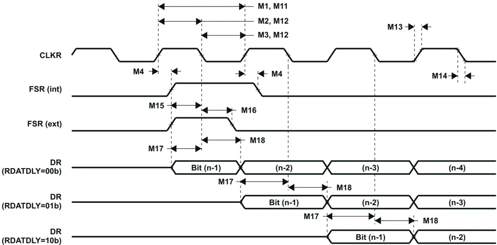
Figure 8-39. McBSP Receive Timing
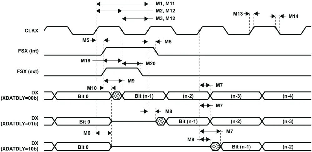
Figure 8-40. McBSP Transmit Timing
78 Submit Document Feedback Copyright © 2021 Texas Instruments Incorporated Product Folder Links: TMS320F2810 TMS320F2810-Q1 TMS320F2811 TMS320F2811-Q1 TMS320F2812 TMS320F2812-Q1
8.12.5.16.2 McBSP as SPI Master or Slave Timing
8.12.5.16.2.1 McBSP as SPI Master or Slave Timing Requirements (CLKSTP = 10b, CLKXP = 0)
| NO.(1) (2) | PARAMETER | MASTER | SLAVE | UNIT | ||
|---|---|---|---|---|---|---|
| MIN | MAX | MIN | MAX | |||
| M30 | tsu(DRV-CKXL) Setup time, DR valid before CLKX low | 30 | 8P – 10 | ns | ||
| M31 | th(CKXL-DRV) Hold time, DR valid after CLKX low | 1 | 8P – 10 | ns | ||
| M32 | tsu(BFXL-CKXH) Setup time, FSX low before CLKX high | 8P + 10 | ns | |||
| M33 | tc(CKX) Cycle time, CLKX | 2P | 16P | ns |
(1) For all SPI slave modes, CLKX has to be a minimum of 8 CLKG cycles. Furthermore, CLKG should be LSPCLK/2 by setting CLKSM = CLKGDV = 1.
(2) 2P = 1/CLKG
8.12.5.16.2.2 McBSP as SPI Master or Slave Switching Characteristics (CLKSTP = 10b, CLKXP = 0)
| NO.(1) | PARAMETER | MASTER | SLAVE | UNIT | ||
|---|---|---|---|---|---|---|
| MIN | MAX | MIN | MAX | |||
| M24 | th(CKXL-FXL) Hold time, FSX low after CLKX low | 2P | ns | |||
| M25 | td(FXL-CKXH) Delay time, FSX low to CLKX high | P | ns | |||
| M28 | tdis(FXH-DXHZ) Disable time, DX high impedance following last data bit from FSX high | 6 | 6P + 6 | ns | ||
| M29 | td(FXL-DXV) Delay time, FSX low to DX valid | 6 | 4P + 6 | ns |
(1) 2P = 1/CLKG
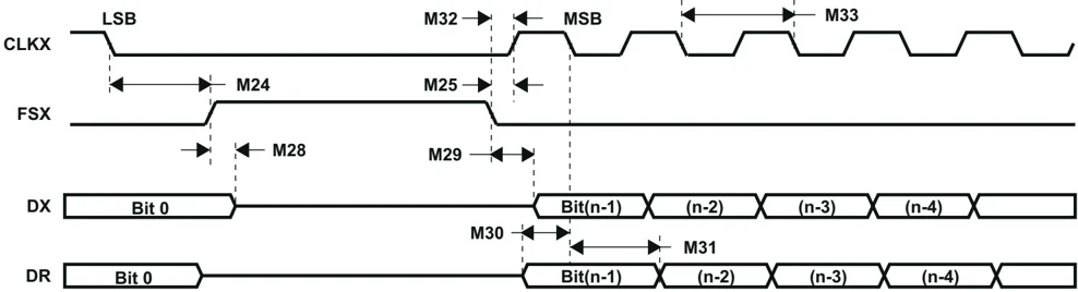
Figure 8-41. McBSP Timing as SPI Master or Slave: CLKSTP = 10b, CLKXP = 0
8.12.5.16.2.3 McBSP as SPI Master or Slave Timing Requirements (CLKSTP = 11b, CLKXP = 0)
| NO.(1) (2) | PARAMETER | MASTER | SLAVE | UNIT |
|---|---|---|---|---|
| MIN MAX | MIN MAX | |||
| M39 | tsu(DRV-CKXH) Setup time, DR valid before CLKX high | 30 | 8P – 10 | ns |
| M40 | th(CKXH-DRV) Hold time, DR valid after CLKX high | 1 | 8P – 10 | ns |
| M41 | tsu(FXL-CKXH) Setup time, FSX low before CLKX high | 16P + 10 | ns | |
| M42 | tc(CKX) Cycle time, CLKX | 2P | 16P | ns |
(1) For all SPI slave modes, CLKX has to be a minimum of 8 CLKG cycles. Furthermore, CLKG should be LSPCLK/2 by setting CLKSM = CLKGDV = 1.
(2) 2P = 1/CLKG
8.12.5.16.2.4 McBSP as SPI Master or Slave Switching Characteristics (CLKSTP = 11b, CLKXP = 0)
| NO.(1) | PARAMETER | MASTER | SLAVE | UNIT |
|---|---|---|---|---|
| MIN MAX | MIN MAX | |||
| M34 | th(CKXL-FXL) Hold time, FSX low after CLKX low | P | ns | |
| M35 | td(FXL-CKXH) Delay time, FSX low to CLKX high | 2P | ns | |
| M37 | tdis(CKXL-DXHZ) Disable time, DX high impedance following last data bit from CLKX low | P + 6 | 7P + 6 | ns |
| M38 | td(FXL-DXV) Delay time, FSX low to DX valid | 6 | 4P + 6 | ns |
(1) 2P = 1/CLKG
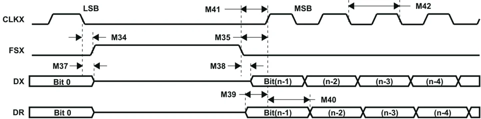
Figure 8-42. McBSP Timing as SPI Master or Slave: CLKSTP = 11b, CLKXP = 0
8.12.5.16.2.5 McBSP as SPI Master or Slave Timing Requirements (CLKSTP = 10b, CLKXP = 1)
| NO.(1) (2) | PARAMETER | MASTER | SLAVE | UNIT | ||
|---|---|---|---|---|---|---|
| MIN | MAX | MIN | MAX | |||
| M49 | tsu(DRV-CKXH) Setup time, DR valid before CLKX high | 30 | 8P – 10 | ns | ||
| M50 | th(CKXH-DRV) Hold time, DR valid after CLKX high | 1 | 8P – 10 | ns | ||
| M51 | tsu(FXL-CKXL) Setup time, FSX low before CLKX low | 8P + 10 | ns | |||
| M52 | tc(CKX) Cycle time, CLKX | 2P | 16P | ns |
(1) For all SPI slave modes, CLKX has to be a minimum of 8 CLKG cycles. Furthermore, CLKG should be LSPCLK/2 by setting CLKSM = CLKGDV = 1.
(2) 2P = 1/CLKG
8.12.5.16.2.6 McBSP as SPI Master or Slave Switching Characteristics (CLKSTP = 10b, CLKXP = 1)
| NO.(1) | PARAMETER | MASTER | SLAVE | UNIT | ||
|---|---|---|---|---|---|---|
| MIN | MAX | MIN | MAX | |||
| M43 | th(CKXH-FXL) Hold time, FSX low after CLKX high | 2P | ns | |||
| M44 | td(FXL-CKXL) Delay time, FSX low to CLKX low | P | ns | |||
| M47 | tdis(FXH-DXHZ) Disable time, DX high impedance following last data bit from FSX high | 6 | 6P + 6 | ns | ||
| M48 | td(FXL-DXV) Delay time, FSX low to DX valid | 6 | 4P + 6 | ns |
(1) 2P = 1/CLKG
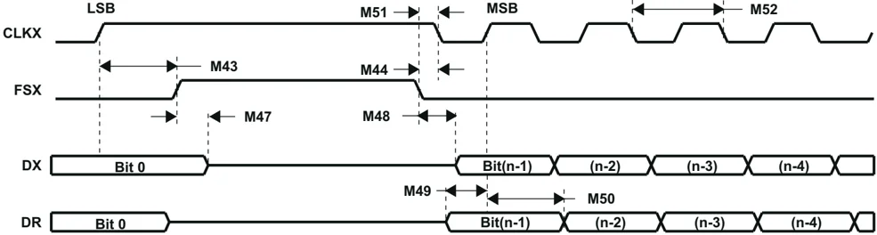
Figure 8-43. McBSP Timing as SPI Master or Slave: CLKSTP = 10b, CLKXP = 1
8.12.5.16.2.7 McBSP as SPI Master or Slave Timing Requirements (CLKSTP = 11b, CLKXP = 1)
| NO.(1) (2) | PARAMETER | MASTER | SLAVE | UNIT | ||
|---|---|---|---|---|---|---|
| MIN | MAX | MIN | MAX | |||
| M58 | tsu(DRV-CKXL) Setup time, DR valid before CLKX low | 30 | 8P – 10 | ns | ||
| M59 | th(CKXL-DRV) Hold time, DR valid after CLKX low | 1 | 8P – 10 | ns | ||
| M60 | tsu(FXL-CKXL) Setup time, FSX low before CLKX low | 16P + 10 | ns | |||
| M61 | tc(CKX) Cycle time, CLKX | 2P | 16P | ns |
(1) For all SPI slave modes, CLKX has to be a minimum of 8 CLKG cycles. Furthermore, CLKG should be LSPCLK/2 by setting CLKSM = CLKGDV = 1.
(2) 2P = 1/CLKG
8.12.5.16.2.8 McBSP as SPI Master or Slave Switching Characteristics (CLKSTP = 11b, CLKXP = 1)
| NO.(1) | PARAMETER | MASTER | SLAVE | UNIT | ||
|---|---|---|---|---|---|---|
| MIN | MAX | MIN | MAX | |||
| M53 | th(CKXH-FXL) Hold time, FSX low after CLKX high | P | ns | |||
| M54 | td(FXL-CKXL) Delay time, FSX low to CLKX low | 2P | ns | |||
| M55 | td(CLKXH-DXV) Delay time, CLKX high to DX valid | –2 | 0 | 3P + 6 | 5P + 20 | ns |
| M56 | tdis(CKXH-DXHZ) Disable time, DX high impedance following last data bit from CLKX high | P + 6 | 7P + 6 | ns | ||
| M57 | td(FXL-DXV) Delay time, FSX low to DX valid | 6 | 4P + 6 | ns |
(1) 2P = 1/CLKG
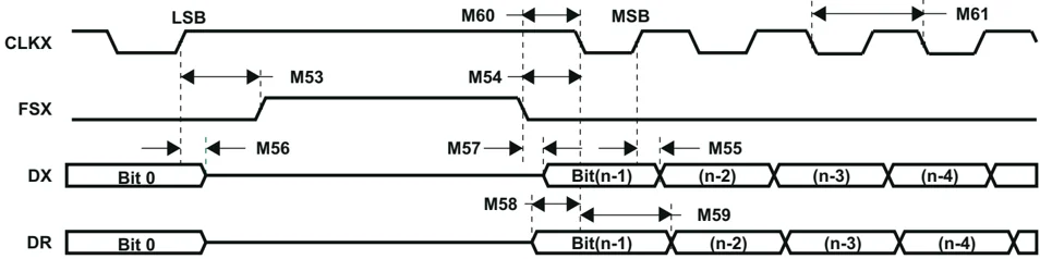
Figure 8-44. McBSP Timing as SPI Master or Slave: CLKSTP = 11b, CLKXP = 1
8.12.6 Emulator Connection Without Signal Buffering for the DSP
Figure 8-45 shows the connection between the DSP and JTAG header for a single-processor configuration. If the distance between the JTAG header and the DSP is greater than 6 inches, the emulation signals must be buffered. If the distance is less than 6 inches, buffering is typically not needed. Figure 8-45 shows the simpler, no-buffering situation. For the pullup/pulldown resistor values, see the pin description section.
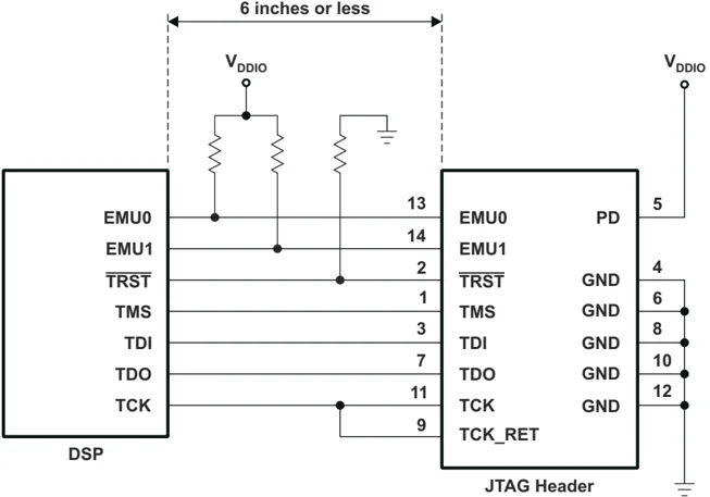
Figure 8-45. Emulator Connection Without Signal Buffering for the DSP
8.12.7 Interrupt Timing
8.12.7.1 Interrupt Switching Characteristics
| PARAMETER | MIN | MAX | UNIT |
|---|---|---|---|
| td(PDP-PWM)HZ Delay time, PDPINTx low to PWM high-impedance state | Without input qualifier | 12 | ns |
| With input qualifier | 1tc(SCO) + IQT + 12(1) | ||
| td(TRIP-PWM)HZ Delay time, CxTRIP/ TxCTRIП signals low to PWM high-impedance state | Without input qualifier | 3 * tc(SCO) | ns |
| With input qualifier | 2tc(SCO) + IQT(1) | ||
| td(INT) Delay time, INT low/high to interrupt-vector fetch | IQT + 12tc(SCO) (1) | ns |
(1) Input Qualification Time (IQT) = [tc(SCO) × 2 × QUALPRD] × 5 + [tc(SCO) × 2 × QUALPRD].
8.12.7.2 Interrupt Timing Requirements
| MIN | MAX | UNIT | ||
|---|---|---|---|---|
| tw(INT) Pulse duration, INT input low/high | With no qualifier | 2tc(SCO) | cycles | |
| With qualifier | 1tc(SCO) + IQT(1) | |||
| tw(PDP) Pulse duration, PDPINTx input low | With no qualifier | 2tc(SCO) | cycles | |
| With qualifier | 1tc(SCO) + IQT(1) | |||
| tw(CxTRIP) Pulse duration, CxTRIP input low | With no qualifier | 2tc(SCO) | cycles | |
| With qualifier | 1tc(SCO) + IQT(1) | |||
| tw(TxCTRIП) Pulse duration, TxCTRIП input low | With no qualifier | 2tc(SCO) | cycles | |
| With qualifier | 1tc(SCO) + IQT(1) |
(1) Input Qualification Time (IQT) = [tc(SCO) × 2 × QUALPRD] × 5 + [tc(SCO) × 2 × QUALPRD].
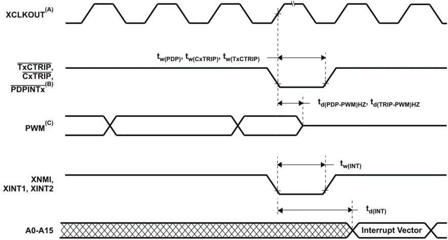
A. XCLKOUT = SYSCLKOUT B. TxCTRIП – T1CTRIП, T2CTRIП, T3CTRIП, T4CTRIП CxTRIP – C1TRIP, C2TRIP, C3TRIP, C4TRIP, C5TRIP, or C6TRIP PDPINTx – PDPINTA or PDPINTB C. PWM refers to all the PWM pins in the device (that is, PWMn and TnPWM pins or PWM pin pair relevant to each CxTRIP pin). The state of the PWM pins after PDPINTx is taken high depends on the state of the FCOMPOE bit.
Figure 8-46. External Interrupt Timing
8.12.8 Flash Timing
8.12.8.1 Flash Endurance for A and S Temperature Material
| ERASE/PROGRAM TEMPERATURE(1) | MIN | TYP | MAX | UNIT | |
|---|---|---|---|---|---|
| Nf Flash endurance for the array (Write/Erase cycles) | 0°C to 85°C (ambient) | 20000(2) | 50000(2) | cycles | |
| NOTP OTP endurance for the array (Write cycles) | 0°C to 85°C (ambient) | 1 | write |
(1) Write/erase operations outside of the temperature ranges indicated are not specified and may affect the endurance numbers.
(2) The Write/Erase cycle numbers of 20000 (MIN) and 50000 (TYP) are applicable only for silicon revision G. For older silicon revisions, the Write/Erase cycle numbers of 100 (MIN) and 1000 (TYP) are applicable.
8.12.8.2 Flash Endurance for Q Temperature Material
| ERASE/PROGRAM TEMPERATURE(1) | MIN | TYP | MAX | UNIT | |
|---|---|---|---|---|---|
| Nf Flash endurance for the array (Write/Erase cycles) | –40°C to 125°C (ambient) | 20000(2) | 50000(2) | cycles | |
| NOTP OTP endurance for the array (Write cycles) | –40°C to 125°C (ambient) | 1 | write |
(1) Write/erase operations outside of the temperature ranges indicated are not specified and may affect the endurance numbers.
(2) The Write/Erase cycle numbers of 20000 (MIN) and 50000 (TYP) are applicable only for silicon revision G. For older silicon revisions, the Write/Erase cycle numbers of 100 (MIN) and 1000 (TYP) are applicable.
8.12.8.3 Flash Parameters at 150-MHz SYSCLKOUT
| PARAMETER(1) | MIN | TYP | MAX | UNIT | ||
|---|---|---|---|---|---|---|
| Program Time | 16-Bit Word | Using Flash API v1(2) | 35 | µs | ||
| Using Flash API v2.10 | 50 | |||||
| 8K Sector | Using Flash API v1(2) | 170 | ms | |||
| Using Flash API v2.10 | 250 | |||||
| 16K Sector | Using Flash API v1(2) | 320 | ms | |||
| Using Flash API v2.10 | 500 | |||||
| Erase Time(3) | 8K Sector | 10 | s | |||
| 16K Sector | 11 | |||||
| IDD3VFLP VDD3VFL current consumption during the Erase/Program cycle | Erase | 75 | mA | |||
| Program | 35 | |||||
| IDDP VDD current consumption during Erase/Program cycle | 140 | mA | ||||
| IDDIOP VDDIO current consumption during Erase/Program cycle | 20 | mA |
(1) Typical parameters as seen at room temperature including function call overhead, with all peripherals off. It is important to maintain a stable power supply during the entire flash programming process. It is conceivable that device current consumption during flash programming could be higher than normal operating conditions. The power supply used should ensure VMIN on the supply rails at all times, as specified in the Recommended Operating Conditions of the data sheet. Any brown-out or interruption to power during erasing/programming could potentially corrupt the password locations and lock the device permanently. Powering a target board (during flash programming) through the USB port is not recommended, as the port may be unable to respond to the power demands placed during the programming process.
(2) Flash API v1.00 is useable on rev. C silicon only.
(3) The on-chip flash memory is in an erased state when the device is shipped from TI. As such, erasing the flash memory is not required prior to programming, when programming the device for the first time. However, the erase operation is needed on all subsequent programming operations.

8.12.8.4 Flash/OTP Access Timing
| PARAMETER | MIN | MAX | UNIT |
|---|---|---|---|
| ta(fp) | Paged Flash access time | 36 | ns |
| ta(fr) | Random Flash access time | 36 | ns |
| ta(OTP) | OTP access time | 60 | ns |
8.12.8.5 Flash Data Retention Duration
| PARAMETER | TEST CONDITIONS | MIN | MAX | UNIT |
|---|---|---|---|---|
| tretention | Data retention duration | TJ = 55°C | 15 | years |
Table 8-5. Minimum Required Flash Wait States at Different Frequencies
| SYSCLKOUT (MHz) | SYSCLKOUT (ns) | PAGE WAIT STATE(1) | RANDOM WAIT STATE(1) (2) | OTP |
|---|---|---|---|---|
| 150 | 6.67 | 5 | 5 | 8 |
| 120 | 8.33 | 4 | 4 | 7 |
| 100 | 10 | 3 | 3 | 5 |
| 75 | 13.33 | 2 | 2 | 4 |
| 50 | 20 | 1 | 1 | 2 |
| 30 | 33.33 | 1 | 1 | 1 |
| 25 | 40 | 0 | 1 | 1 |
| 15 | 66.67 | 0 | 1 | 1 |
| 4 | 250 | 0 | 1 | 1 |
(1) Formulas to compute page wait state and random wait state:
Flash Page Wait State = \left\lceil \left( \fract_a(fp)t_c(SCO) \right) - 1 \right\rceil (round up to the next highest integer, or 0, whichever is larger)
Flash Random Wait State = \left\lceil \left( \fract_a(fr)t_c(SCO) \right) - 1 \right\rceil (round up to the next highest integer, or 1, whichever is larger)
OTP Wait State = \left\lceil \left( \fract_a(OTP)t_c(SCO) \right) - 1 \right\rceil (round up to the next highest integer, or 1, whichever is larger)
(2) Random wait state must be greater than or equal to 1.