9 Detailed Description
9.1 Brief Descriptions
9.1.1 C28x CPU
The C28x DSP generation is the newest member of the TMS320C2000™ DSP platform. The C28x is source code compatible to the 24x/240x DSP devices, hence existing 240x users can leverage their significant software investment. Additionally, the C28x is a very efficient C/C++ engine, enabling users to develop not only their system control software in a high-level language, but also enables math algorithms to be developed using C/C++. The C28x is as efficient in DSP math tasks as it is in system control tasks that typically are handled by microcontroller devices. This efficiency removes the need for a second processor in many systems. The 32 x 32-bit MAC capabilities of the C28x and its 64-bit processing capabilities, enable the C28x to efficiently handle higher numerical resolution problems that would otherwise demand a more expensive floating-point processor solution. Add to this the fast interrupt response with automatic context save of critical registers, resulting in a device that is capable of servicing many asynchronous events with minimal latency. The C28x has an 8-level-deep protected pipeline with pipelined memory accesses. This pipelining enables the C28x to execute at high speeds without resorting to expensive high-speed memories. Special branch-look-ahead hardware minimizes the latency for conditional discontinuities. Special store conditional operations further improve performance.
9.1.2 Memory Bus (Harvard Bus Architecture)
As with many DSP type devices, multiple busses are used to move data between the memories and peripherals and the CPU. The C28x memory bus architecture contains a program read bus, data read bus and data write bus. The program read bus consists of 22 address lines and 32 data lines. The data read and write busses consist of 32 address lines and 32 data lines each. The 32-bit-wide data busses enable single cycle 32-bit operations. The multiple bus architecture, commonly termed “Harvard Bus”, enables the C28x to fetch an instruction, read a data value and write a data value in a single cycle. All peripherals and memories attached to the memory bus will prioritize memory accesses. Generally, the priority of Memory Bus accesses can be summarized as follows:
Highest:
- Data Writes (Simultaneous data and program writes cannot occur on the memory bus.)
- Program Writes (Simultaneous data and program writes cannot occur on the memory bus.)
- Data Reads
- Program Reads (Simultaneous program reads and fetches cannot occur on the memory bus.)
Lowest:
- Fetches (Simultaneous program reads and fetches cannot occur on the memory bus.)
9.1.3 Peripheral Bus
To enable migration of peripherals between various Texas Instruments (TI) DSP family of devices, the F281x adopts a peripheral bus standard for peripheral interconnect. The peripheral bus bridge multiplexes the various busses that make up the processor “Memory Bus” into a single bus consisting of 16 address lines and 16 or 32 data lines and associated control signals. Two versions of the peripheral bus are supported on the F281x. One version only supports 16-bit accesses (called peripheral frame 2). The other version supports both 16- and 32-bit accesses (called peripheral frame 1).
9.1.4 Real-Time JTAG and Analysis
The F281x implements the standard IEEE 1149.1 JTAG interface. Additionally, the F281x supports real-time mode of operation whereby the contents of memory, peripheral, and register locations can be modified while the processor is running and executing code and servicing interrupts. The user can also single step through non-time critical code while enabling time-critical interrupts to be serviced without interference. The F281x implements the real-time mode in hardware within the CPU. This is a unique feature to the F281x, no software monitor is required. Additionally, special analysis hardware is provided that allows the user to set hardware breakpoint or data/address watch-points and generate various user selectable break events when a match occurs.

9.1.5 External Interface (XINTF) (F2812 Only)
This asynchronous interface consists of 19 address lines, 16 data lines, and three chip-select lines. The chip-select lines are mapped to five external zones, Zones 0, 1, 2, 6, and 7. Zones 0 and 1 share a single chip-select; Zones 6 and 7 also share a single chip-select. Each of the five zones can be programmed with a different number of wait states, strobe signal setup and hold timing and each zone can be programmed for extending wait states externally or not. The programmable wait-state, chip-select and programmable strobe timing enables glueless interface to external memories and peripherals.
9.1.6 Flash
The F2812 and F2811 contain 128K x 16 of embedded flash memory, segregated into four 8K x 16 sectors, and six 16K x 16 sectors. The F2810 has 64K x 16 of embedded flash, segregated into two 8K x 16 sectors, and three 16K x 16 sectors. All three devices also contain a single 1K x 16 of OTP memory at address range 0x3D 7800–0x3D 7BFF. The user can individually erase, program, and validate a flash sector while leaving other sectors untouched. However, it is not possible to use one sector of the flash or the OTP to execute flash algorithms that erase/program other sectors. Special memory pipelining is provided to enable the flash module to achieve higher performance. The flash/OTP is mapped to both program and data space; therefore, it can be used to execute code or store data information.
Note
The F2810/F2811/F2812 Flash and OTP wait states can be configured by the application. This allows applications running at slower frequencies to configure the flash to use fewer wait states.
Flash effective performance can be improved by enabling the flash pipeline mode in the Flash options register. With this mode enabled, effective performance of linear code execution will be much faster than the raw performance indicated by the wait state configuration alone. The exact performance gain when using the Flash pipeline mode is application-dependent.
For more information on the Flash options, Flash wait-state, and OTP wait-state registers, see the TMS320x281x DSP System Control and Interrupts Reference Guide.
9.1.7 M0, M1 SARAMs
All C28x devices contain these two blocks of single access memory, each 1K x 16 in size. The stack pointer points to the beginning of block M1 on reset. The M0 block overlaps the 240x device B0, B1, B2 RAM blocks and hence the mapping of data variables on the 240x devices can remain at the same physical address on C28x devices. The M0 and M1 blocks, like all other memory blocks on C28x devices, are mapped to both program and data space. Hence, the user can use M0 and M1 to execute code or for data variables. The partitioning is performed within the linker. The C28x device presents a unified memory map to the programmer. This makes for easier programming in high-level languages.
9.1.8 L0, L1, H0 SARAMs
The F281x contains an additional 16K x 16 of single-access RAM, divided into three blocks (4K + 4K + 8K). Each block can be independently accessed hence minimizing pipeline stalls. Each block is mapped to both program and data space.
9.1.9 Boot ROM
The Boot ROM is factory-programmed with boot-loading software. The Boot ROM program executes after device reset and checks several GPIO pins to determine which boot mode to enter. For example, the user can select to execute code already present in the internal Flash or download new software to internal RAM through one of several serial ports. Other boot modes exist as well. The Boot ROM also contains standard tables, such as SIN/COS waveforms, for use in math-related algorithms. Table 9-1 shows the details of how various boot modes may be invoked. See the TMS320x281x DSP Boot ROM Reference Guide, for more information.

Table 9-1. Boot Mode Selection
| BOOT MODE SELECTED(1) (2) | GPIOF4 (SCITXDA) | GPIOF12 (MDXA) | GPIOF3 (SPISTEA) | GPIOF2 (SPICLK) |
|---|---|---|---|---|
| GPIO PU status(3) | PU | No PU | No PU | No PU |
| Jump to Flash address 0x3F 7FF6. A branch instruction must have been programmed here prior to reset to re-direct code execution as desired. | 1 | x | x | x |
| Call SPI_Boot to load from an external serial SPI EEPROM | 0 | 1 | x | x |
| Call SCI_Boot to load from SCI-A | 0 | 0 | 1 | 1 |
| Jump to H0 SARAM address 0x3F 8000 | 0 | 0 | 1 | 0 |
| Jump to OTP address 0x3D 7800 | 0 | 0 | 0 | 1 |
| Call Parallel_Boot to load from GPIO Port B | 0 | 0 | 0 | 0 |
(1) Extra care must be taken due to any effect toggling SPICLK to select a boot mode may have on external logic.
(2) If the boot mode selected is Flash, H0, or OTP, then no external code is loaded by the bootloader.
(3) PU = pin has an internal pullup. No PU = pin does not have an internal pullup.

9.1.10 Security
The F281x supports high levels of security to protect the user firmware from being reverse-engineered. The security features a 128-bit password (hardcoded for 16 wait states), which the user programs into the flash. One code security module (CSM) is used to protect the flash/OTP and the L0/L1 SARAM blocks. The security feature prevents unauthorized users from examining the memory contents via the JTAG port, executing code from external memory or trying to boot-load some undesirable software that would export the secure memory contents. To enable access to the secure blocks, the user must write the correct 128-bit "KEY" value, which matches the value stored in the password locations within the Flash.
Note
- When the code-security passwords are programmed, all addresses between 0x3F 7F80 and 0x3F 7FF5 cannot be used as program code or data. These locations must be programmed to 0x0000.
- If the code security feature is not used, addresses 0x3F 7F80 through 0x3F 7FEF may be used for code or data.
- The 128-bit password (at 0x3F 7FF8–0x3F 7FFF) must not be programmed to zeros. Doing so would permanently lock the device.
Table 9-2. Impact of Using the Code Security Module
| ADDRESS | CODE SECURITY STATUS | |
|---|---|---|
| Code Security Enabled | Code Security Disabled | |
| 0x3F 7F80 – 0x3F 7FEF | Fill with 0x0000 | Application code and data(1) |
| 0x3F 7FF0 – 0x3F 7FF5 | ||
| 0x3D 7BFC – 0x3D 7BFF | Application code and data |
(1) See the TMS320F281x DSPs Silicon Errata for some restrictions.
Note
Code Security Module Disclaimer
THE CODE SECURITY MODULE (CSM) INCLUDED ON THIS DEVICE WAS DESIGNED TO PASSWORD PROTECT THE DATA STORED IN THE ASSOCIATED MEMORY (EITHER ROM OR FLASH) AND IS WARRANTED BY TEXAS INSTRUMENTS (TI), IN ACCORDANCE WITH ITS STANDARD TERMS AND CONDITIONS, TO CONFORM TO TI'S PUBLISHED SPECIFICATIONS FOR THE WARRANTY PERIOD APPLICABLE FOR THIS DEVICE.
TI DOES NOT, HOWEVER, WARRANT OR REPRESENT THAT THE CSM CANNOT BE COMPROMISED OR BREACHED OR THAT THE DATA STORED IN THE ASSOCIATED MEMORY CANNOT BE ACCESSED THROUGH OTHER MEANS. MOREOVER, EXCEPT AS SET FORTH ABOVE, TI MAKES NO WARRANTIES OR REPRESENTATIONS CONCERNING THE CSM OR OPERATION OF THIS DEVICE, INCLUDING ANY IMPLIED WARRANTIES OF MERCHANTABILITY OR FITNESS FOR A PARTICULAR PURPOSE.
IN NO EVENT SHALL TI BE LIABLE FOR ANY CONSEQUENTIAL, SPECIAL, INDIRECT, INCIDENTAL, OR PUNITIVE DAMAGES, HOWEVER CAUSED, ARISING IN ANY WAY OUT OF YOUR USE OF THE CSM OR THIS DEVICE, WHETHER OR NOT TI HAS BEEN ADVISED OF THE POSSIBILITY OF SUCH DAMAGES. EXCLUDED DAMAGES INCLUDE, BUT ARE NOT LIMITED TO LOSS OF DATA, LOSS OF GOODWILL, LOSS OF USE OR INTERRUPTION OF BUSINESS OR OTHER ECONOMIC LOSS.
Product Folder Links: TMS320F2810 TMS320F2810-Q1 TMS320F2811 TMS320F2811-Q1 TMS320F2812 TMS320F2812-Q1
9.1.11 Peripheral Interrupt Expansion (PIE) Block
The PIE block serves to multiplex numerous interrupt sources into a smaller set of interrupt inputs. The PIE block can support up to 96 peripheral interrupts. On the F281x, 45 of the possible 96 interrupts are used by peripherals. The 96 interrupts are grouped into blocks of 8 and each group is fed into 1 of 12 CPU interrupt lines (INT1 to INT12). Each of the 96 interrupts is supported by its own vector stored in a dedicated RAM block that can be overwritten by the user. The vector is automatically fetched by the CPU on servicing the interrupt. It takes 8 CPU clock cycles to fetch the vector and save critical CPU registers. Hence the CPU can quickly respond to interrupt events. Prioritization of interrupts is controlled in hardware and software. Each individual interrupt can be enabled/disabled within the PIE block.
9.1.12 External Interrupts (XINT1, XINT2, XINT13, XNMI)
The F281x supports three masked external interrupts (XINT1, 2, 13). XINT13 is combined with one non-masked external interrupt (XNMI). The combined signal name is XNMI_XINT13. Each of the interrupts can be selected for negative or positive edge triggering and can also be enabled/disabled (including the XNMI). The masked interrupts also contain a 16-bit free-running up-counter, which is reset to zero when a valid interrupt edge is detected. This counter can be used to accurately time-stamp the interrupt.
9.1.13 Oscillator and PLL
The F281x can be clocked by an external oscillator or by a crystal attached to the on-chip oscillator circuit. A PLL is provided supporting up to 10-input clock-scaling ratios. The PLL ratios can be changed on-the-fly in software, enabling the user to scale back on operating frequency if lower power operation is desired. Refer to Section 8 for timing details. The PLL block can be set in bypass mode.
9.1.14 Watchdog
The F281x supports a watchdog timer. The user software must regularly reset the watchdog counter within a certain time frame; otherwise, the watchdog will generate a reset to the processor. The watchdog can be disabled if necessary.
9.1.15 Peripheral Clocking
The clocks to each individual peripheral can be enabled/disabled to reduce power consumption when a peripheral is not in use. Additionally, the system clock to the serial ports (except eCAN) and the event managers, CAP and QEP blocks can be scaled relative to the CPU clock. This enables the timing of peripherals to be decoupled from increasing CPU clock speeds.
9.1.16 Low-Power Modes
The F281x devices are fully static CMOS devices. Three low-power modes are provided:
IDLE: Place CPU in low-power mode. Peripheral clocks may be turned off selectively and only those peripherals that must function during IDLE are left operating. An enabled interrupt from an active peripheral will wake the processor from IDLE mode.
STANDBY: Turns off clock to CPU and peripherals. This mode leaves the oscillator and PLL functional. An external interrupt event will wake the processor and the peripherals. Execution begins on the next valid cycle after detection of the interrupt event.
HALT: Turns off the internal oscillator. This mode basically shuts down the device and places it in the lowest possible power consumption mode. Only a reset or XNMI can wake the device from this mode.

9.1.17 Peripheral Frames 0, 1, 2 (PFn)
The F281x segregates peripherals into three sections. The mapping of peripherals is as follows:
PF0:
- XINTF: External Interface Configuration Registers (F2812 only)
- PIE: PIE Interrupt Enable and Control Registers Plus PIE Vector Table
- Flash: Flash Control, Programming, Erase, Verify Registers
- Timers: CPU-Timers 0, 1, 2 Registers
- CSM: Code Security Module KEY Registers
PF1:
- eCAN: eCAN Mailbox and Control Registers
PF2:
- SYS: System Control Registers
- GPIO: GPIO Mux Configuration and Control Registers
- EV: Event Manager (EVA/EVB) Control Registers
- McBSP: McBSP Control and TX/RX Registers
- SCI: Serial Communications Interface (SCI) Control and RX/TX Registers
- SPI: Serial Peripheral Interface (SPI) Control and RX/TX Registers
- ADC: 12-Bit ADC Registers
9.1.18 General-Purpose Input/Output (GPIO) Multiplexer
Most of the peripheral signals are multiplexed with general-purpose I/O (GPIO) signals. This multiplexing enables use of a pin as GPIO if the peripheral signal or function is not used. On reset, all GPIO pins are configured as inputs. The user can then individually program each pin for GPIO mode or peripheral signal mode. For specific inputs, the user can also select the number of input qualification cycles to filter unwanted noise glitches.
9.1.19 32-Bit CPU-Timers (0, 1, 2)
CPU-Timers 0, 1, and 2 are identical 32-bit timers with presettable periods and with 16-bit clock prescaling. The timers have a 32-bit count-down register, which generates an interrupt when the counter reaches zero. The counter is decremented at the CPU clock speed divided by the prescale value setting. When the counter reaches zero, it is automatically reloaded with a 32-bit period value. CPU-Timer 2 is reserved for the DSP/BIOS Real-Time OS, and is connected to INT14 of the CPU. If DSP/BIOS is not being used, CPU-Timer 2 is available for general use. CPU-Timer 1 is for general use and can be connected to INT13 of the CPU. CPU-Timer 0 is also for general use and is connected to the PIE block.
9.1.20 Control Peripherals
The F281x supports the following peripherals that are used for embedded control and communication:
EV: The event manager module includes general-purpose timers, full-compare/PWM units, capture inputs (CAP) and quadrature-encoder pulse (QEP) circuits. Two such event managers are provided which enable two three-phase motors to be driven or four two-phase motors. The event managers on the F281x are compatible to the event managers on the 240x devices (with some minor enhancements).
ADC: The ADC block is a 12-bit converter, single ended, 16-channels. It contains two sample-and-hold units for simultaneous sampling.
9.1.21 Serial Port Peripherals
The F281x supports the following serial communication peripherals:
eCAN: This is the enhanced version of the CAN peripheral. It supports 32 mailboxes, time stamping of messages, and is compliant with ISO 11898-1 (CAN 2.0B).
McBSP: The multichannel buffered serial port (McBSP) connects to E1/T1 lines, phone-quality codecs for modem applications or high-quality stereo audio DAC devices. The McBSP receive and transmit registers are supported by a 16-level FIFO that significantly reduces the overhead for servicing this peripheral.
SPI: The SPI is a high-speed, synchronous serial I/O port that allows a serial bit stream of programmed length (one to sixteen bits) to be shifted into and out of the device at a programmable bit-transfer rate. Normally, the SPI is used for communications between the DSP controller and external peripherals or another processor. Typical applications include external I/O or peripheral expansion through devices such as shift registers, display drivers, and ADCs. Multi-device communications are supported by the master/slave operation of the SPI. On the F281x, the port supports a 16-level, receive-and-transmit FIFO for reducing servicing overhead.
SCI: The serial communications interface is a two-wire asynchronous serial port, commonly known as UART. On the F281x, the port supports a 16-level, receive-and-transmit FIFO for reducing servicing overhead.
9.2 Peripherals
The integrated peripherals of the F281x are described in the following subsections:
- Three 32-bit CPU-Timers
- Two event-manager modules (EVA, EVB)
- Enhanced analog-to-digital converter (ADC) module
- Enhanced controller area network (eCAN) module
- Multichannel buffered serial port (McBSP) module
- Serial communications interface modules (SCI-A, SCI-B)
- Serial peripheral interface (SPI) module
- Digital I/O and shared pin functions
9.2.1 32-Bit CPU-Timers 0/1/2
There are three 32-bit CPU-timers on the F281x devices (CPU-TIMER0/1/2).
Timer 2 is reserved for DSP/BIOS. CPU-Timer 0 and CPU-Timer 1 can be used in user applications. These timers are different from the general-purpose (GP) timers that are present in the Event Manager modules (EVA, EVB).
Note
If the application is not using DSP/BIOS, then CPU-Timer 2 can be used in the application.
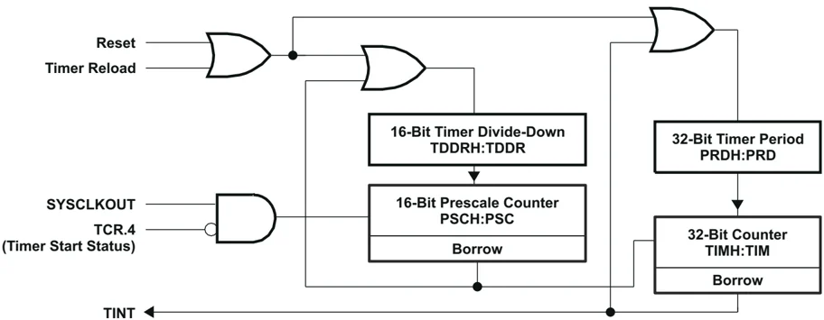
Figure 9-1. CPU-Timers
In the F281x devices, the timer interrupt signals (TINT0, TINT1, TINT2) are connected as shown in Figure 9-2.
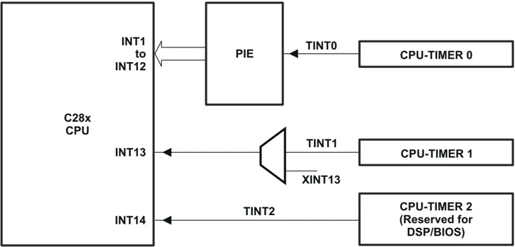
A. The timer registers are connected to the memory bus of the C28x processor. B. The timing of the timers is synchronized to SYSCLKOUT of the processor clock.
Figure 9-2. CPU-Timer Interrupts Signals and Output Signal
The general operation of the timer is as follows: The 32-bit counter register "TIMH:TIM" is loaded with the value in the period register "PRDH:PRD". The counter register decrements at the SYSCLKOUT rate of the C28x. When the counter reaches 0, a timer interrupt output signal generates an interrupt pulse. The registers listed in Table 9-3 are used to configure the timers. For more information, see the TMS320x281x DSP System Control and Interrupts Reference Guide.
Table 9-3. CPU-Timers 0, 1, 2 Configuration and Control Registers
| NAME | ADDRESS | SIZE (x16) | DESCRIPTION |
|---|---|---|---|
| TIMER0TIM | 0x00 0C00 | 1 | CPU-Timer 0, Counter Register |
| TIMER0TIMH | 0x00 0C01 | 1 | CPU-Timer 0, Counter Register High |
| TIMER0PRD | 0x00 0C02 | 1 | CPU-Timer 0, Period Register |
| TIMER0PRDH | 0x00 0C03 | 1 | CPU-Timer 0, Period Register High |
| TIMER0TCR | 0x00 0C04 | 1 | CPU-Timer 0, Control Register |
| Reserved | 0x00 0C05 | 1 | |
| TIMER0TPR | 0x00 0C06 | 1 | CPU-Timer 0, Prescale Register |
| TIMER0TPRH | 0x00 0C07 | 1 | CPU-Timer 0, Prescale Register High |
| TIMER1TIM | 0x00 0C08 | 1 | CPU-Timer 1, Counter Register |
| TIMER1TIMH | 0x00 0C09 | 1 | CPU-Timer 1, Counter Register High |
| TIMER1PRD | 0x00 0C0A | 1 | CPU-Timer 1, Period Register |
| TIMER1PRDH | 0x00 0C0B | 1 | CPU-Timer 1, Period Register High |
| TIMER1TCR | 0x00 0C0C | 1 | CPU-Timer 1, Control Register |
| Reserved | 0x00 0C0D | 1 | |
| TIMER1TPR | 0x00 0C0E | 1 | CPU-Timer 1, Prescale Register |
| TIMER1TPRH | 0x00 0C0F | 1 | CPU-Timer 1, Prescale Register High |
| TIMER2TIM | 0x00 0C10 | 1 | CPU-Timer 2, Counter Register |
| TIMER2TIMH | 0x00 0C11 | 1 | CPU-Timer 2, Counter Register High |
| TIMER2PRD | 0x00 0C12 | 1 | CPU-Timer 2, Period Register |
| TIMER2PRDH | 0x00 0C13 | 1 | CPU-Timer 2, Period Register High |
| TIMER2TCR | 0x00 0C14 | 1 | CPU-Timer 2, Control Register |
| Reserved | 0x00 0C15 | 1 | |
| TIMER2TPR | 0x00 0C16 | 1 | CPU-Timer 2, Prescale Register |
| TIMER2TPRH | 0x00 0C17 | 1 | CPU-Timer 2, Prescale Register High |
| Reserved | 0x00 0C18 – 0x00 0C3F | 40 |
9.2.2 Event Manager Modules (EVA, EVB)
The event-manager modules include general-purpose (GP) timers, full-compare/PWM units, capture units, and quadrature-encoder pulse (QEP) circuits. EVA and EVB timers, compare units, and capture units function identically. However, timer/unit names differ for EVA and EVB. Table 9-4 shows the module and signal names used. Table 9-4 shows the features and functionality available for the event-manager modules and highlights EVA nomenclature.
Event managers A and B have identical peripheral register sets with EVA starting at 7400h and EVB starting at 7500h. The paragraphs in this section describe the function of GP timers, compare units, capture units, and QEPs using EVA nomenclature. These paragraphs are applicable to EVB with regard to function—however, module/signal names would differ. Table 9-5 lists the EVA registers. For more information, see the TMS320x281x DSP Event Manager (EV) Reference Guide.
Table 9-4. Module and Signal Names for EVA and EVB
| EVENT MANAGER MODULES | EVA | EVB | ||
|---|---|---|---|---|
| MODULE | SIGNAL | MODULE | SIGNAL | |
| GP Timers | GP Timer 1GP Timer 2 | T1PWM/T1CMPT2PWM/T2CMP | GP Timer 3GP Timer 4 | T3PWM/T3CMPT4PWM/T4CMP |
| Compare Units | Compare 1Compare 2Compare 3 | PWM1/2PWM3/4PWM5/6 | Compare 4Compare 5Compare 6 | PWM7/8PWM9/10PWM11/12 |
| Capture Units | Capture 1Capture 2Capture 3 | CAP1CAP2CAP3 | Capture 4Capture 5Capture 6 | CAP4CAP5CAP6 |
| QEP Channels | QEP1QEP2QEP11 | QEP1QEP2 | QEP3QEP4QEP12 | QEP3QEP4 |
| External Clock Inputs | DirectionExternal Clock | TDIRATCLKINA | DirectionExternal Clock | TDIRBTCLKINB |
| External Trip Inputs | Compare | C1TRIPC2TRIPC3TRIP | Compare | C4TRIPC5TRIPC6TRIP |
| External Trip Inputs | T1CTRI_P_PDPINTA (1)T2CTRI_P/ EVASOC | T3CTRI_P_PDPINTB (1)T4CTRI_P/ EVBSOC |
(1) In the 24x/240x-compatible mode, the T1CTRI_P_PDPINTA pin functions as PDPINTA and the T3CTRI_P_PDPINTB pin functions as PDPINTB.

Table 9-5. EVA Registers
| NAME(1) | ADDRESS | SIZE (x16) | DESCRIPTION |
|---|---|---|---|
| GPTCONA | 0x00 7400 | 1 | GP Timer Control Register A |
| T1CNT | 0x00 7401 | 1 | GP Timer 1 Counter Register |
| T1CMPR | 0x00 7402 | 1 | GP Timer 1 Compare Register |
| T1PR | 0x00 7403 | 1 | GP Timer 1 Period Register |
| T1CON | 0x00 7404 | 1 | GP Timer 1 Control Register |
| T2CNT | 0x00 7405 | 1 | GP Timer 2 Counter Register |
| T2CMPR | 0x00 7406 | 1 | GP Timer 2 Compare Register |
| T2PR | 0x00 7407 | 1 | GP Timer 2 Period Register |
| T2CON | 0x00 7408 | 1 | GP Timer 2 Control Register |
| EXTCONA(2) | 0x00 7409 | 1 | GP Extension Control Register A |
| COMCONA | 0x00 7411 | 1 | Compare Control Register A |
| ACTRA | 0x00 7413 | 1 | Compare Action Control Register A |
| DBTCONA | 0x00 7415 | 1 | Dead-Band Timer Control Register A |
| CMPR1 | 0x00 7417 | 1 | Compare Register 1 |
| CMPR2 | 0x00 7418 | 1 | Compare Register 2 |
| CMPR3 | 0x00 7419 | 1 | Compare Register 3 |
| CAPCONA | 0x00 7420 | 1 | Capture Control Register A |
| CAPFIFOA | 0x00 7422 | 1 | Capture FIFO Status Register A |
| CAP1FIFO | 0x00 7423 | 1 | Two-Level-Deep Capture FIFO Stack 1 |
| CAP2FIFO | 0x00 7424 | 1 | Two-Level-Deep Capture FIFO Stack 2 |
| CAP3FIFO | 0x00 7425 | 1 | Two-Level-Deep Capture FIFO Stack 3 |
| CAP1FBOT | 0x00 7427 | 1 | Bottom Register of Capture FIFO Stack 1 |
| CAP2FBOT | 0x00 7428 | 1 | Bottom Register of Capture FIFO Stack 2 |
| CAP3FBOT | 0x00 7429 | 1 | Bottom Register of Capture FIFO Stack 3 |
| EVAIMRA | 0x00 742C | 1 | Interrupt Mask Register A |
| EVAIMRB | 0x00 742D | 1 | Interrupt Mask Register B |
| EVAIMRC | 0x00 742E | 1 | Interrupt Mask Register C |
| EVAIFRA | 0x00 742F | 1 | Interrupt Flag Register A |
| EVAIFRB | 0x00 7430 | 1 | Interrupt Flag Register B |
| EVAIFRC | 0x00 7431 | 1 | Interrupt Flag Register C |
(1) The EV-B register set is identical except the address range is from 0x00 7500 to 0x00 753F. The above registers are mapped to Zone 2. This space allows only 16-bit accesses. 32-bit accesses produce undefined results.
(2) New register compared to 24x/240x
TEXAS INSTRUMENTS www.ti.com
SPRS174V – APRIL 2001 – REVISED FEBRUARY 2021
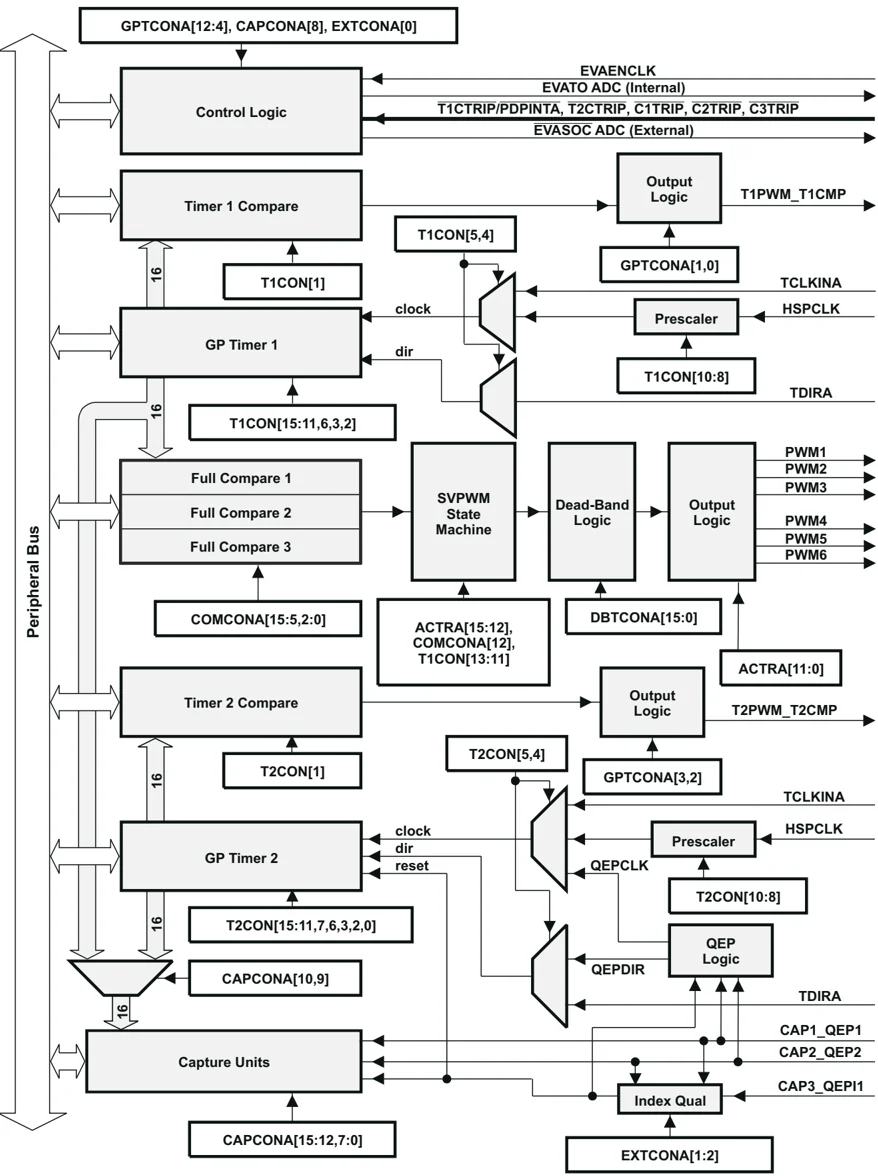
A. The EVB module is similar to the EVA module.
Figure 9-3. Event Manager A Functional Block Diagram
Submit Document Feedback 99 Product Folder Links: TMS320F2810 TMS320F2810-Q1 TMS320F2811 TMS320F2811-Q1 TMS320F2812 TMS320F2812-Q1
9.2.2.1 General-Purpose (GP) Timers
There are two GP timers. The GP timer x (x = 1 or 2 for EVA; x = 3 or 4 for EVB) includes:
- A 16-bit timer, up-/down-counter, TxCNT, for reads or writes
- A 16-bit timer-compare register, TxCMPR (double-buffered with shadow register), for reads or writes
- A 16-bit timer-period register, TxPR (double-buffered with shadow register), for reads or writes
- A 16-bit timer-control register, TxCON, for reads or writes
- Selectable internal or external input clocks
- A programmable prescaler for internal or external clock inputs
- Control and interrupt logic, for four maskable interrupts: underflow, overflow, timer compare, and period interrupts
- A selectable direction input pin (TDIRx) (to count up or down when directional up-/down-count mode is selected)
The GP timers can be operated independently or synchronized with each other. The compare register associated with each GP timer can be used for compare function and PWM-waveform generation. There are three continuous modes of operations for each GP timer in up- or up/down-counting operations. Internal or external input clocks with programmable prescaler are used for each GP timer. GP timers also provide the time base for the other event-manager submodules: GP timer 1 for all the compares and PWM circuits, GP timer 2/1 for the capture units and the quadrature-pulse counting operations. Double-buffering of the period and compare registers allows programmable change of the timer (PWM) period and the compare/PWM pulse width as needed.
9.2.2.2 Full-Compare Units
There are three full-compare units on each event manager. These compare units use GP timer1 as the time base and generate six outputs for compare and PWM-waveform generation using programmable deadband circuit. The state of each of the six outputs is configured independently. The compare registers of the compare units are double-buffered, allowing programmable change of the compare/PWM pulse widths as needed.
9.2.2.3 Programmable Deadband Generator
Deadband generation can be enabled/disabled for each compare unit output individually. The deadband-generator circuit produces two outputs (with or without deadband zone) for each compare unit output signal. The output states of the deadband generator are configurable and changeable as needed by way of the double-buffered ACTRx register.
9.2.2.4 PWM Waveform Generation
Up to eight PWM waveforms (outputs) can be generated simultaneously by each event manager: three independent pairs (six outputs) by the three full-compare units with programmable deadbands, and two independent PWMs by the GP-timer compares.
9.2.2.5 Double Update PWM Mode
The F281x Event Manager supports “Double Update PWM Mode.” This mode refers to a PWM operation mode in which the position of the leading edge and the position of the trailing edge of a PWM pulse are independently modifiable in each PWM period. To support this mode, the compare register that determines the position of the edges of a PWM pulse must allow (buffered) compare value update once at the beginning of a PWM period and another time in the middle of a PWM period. The compare registers in F281x Event Managers are all buffered and support three compare value reload/update (value in buffer becoming active) modes. These modes have earlier been documented as compare value reload conditions. The reload condition that supports double update PWM mode is reloaded on Underflow (beginning of PWM period) OR Period (middle of PWM period). Double update PWM mode can be achieved by using this condition for compare value reload.

9.2.2.6 PWM Characteristics
Characteristics of the PWMs are as follows:
- 16-bit registers
- Wide range of programmable deadband for the PWM output pairs
- Change of the PWM carrier frequency for PWM frequency wobbling as needed
- Change of the PWM pulse widths within and after each PWM period as needed
- External-maskable power and drive-protection interrupts
- Pulse-pattern-generator circuit, for programmable generation of asymmetric, symmetric, and four-space vector PWM waveforms
- Minimized CPU overhead using auto-reload of the compare and period registers
- The PWM pins are driven to a high-impedance state when the PDPINTx pin is driven low and after PDPINTx signal qualification. The PDPINTx pin (after qualification) is reflected in bit 8 of the COMCONx register.
- PDPINTA pin status is reflected in bit 8 of COMCONA register.
- PDPINTB pin status is reflected in bit 8 of COMCONB register.
- EXTCON register bits provide options to individually trip control for each PWM pair of signals
9.2.2.7 Capture Unit
The capture unit provides a logging function for different events or transitions. The values of the selected GP timer counter is captured and stored in the two-level-deep FIFO stacks when selected transitions are detected on capture input pins, CAPx (x = 1, 2, or 3 for EVA; and x = 4, 5, or 6 for EVB). The capture unit consists of three capture circuits.
Capture units include the following features:
- One 16-bit capture control register, CAPCONx (R/W)
- One 16-bit capture FIFO status register, CAPFIFOx
- Selection of GP timer 1/2 (for EVA) or 3/4 (for EVB) as the time base
- Three 16-bit 2-level-deep FIFO stacks, one for each capture unit
- Three capture input pins (CAP1/2/3 for EVA, CAP4/5/6 for EVB)—one input pin per capture unit. [All inputs are synchronized with the device (CPU) clock. In order for a transition to be captured, the input must hold at its current level to meet the input qualification circuitry requirements. The input pins CAP1/2 and CAP4/5 can also be used as QEP inputs to the QEP circuit.]
- User-specified transition (rising edge, falling edge, or both edges) detection
- Three maskable interrupt flags, one for each capture unit
- The capture pins can also be used as general-purpose interrupt pins, if they are not used for the capture function.
9.2.2.8 Quadrature-Encoder Pulse (QEP) Circuit
Two capture inputs (CAP1 and CAP2 for EVA; CAP4 and CAP5 for EVB) can be used to interface the on-chip QEP circuit with a quadrature encoder pulse. Full synchronization of these inputs is performed on-chip. Direction or leading-quadrature pulse sequence is detected, and GP timer 2/4 is incremented or decremented by the rising and falling edges of the two input signals (four times the frequency of either input pulse).
With EXTCONA register bits, the EVA QEP circuit can use CAP3 as a capture index pin as well. Similarly, with EXTCONB register bits, the EVB QEP circuit can use CAP6 as a capture index pin.
9.2.2.9 External ADC Start-of-Conversion
EVA/EVB start-of-conversion (SOC) can be sent to an external pin (EVASOC/ EVBSOC) for external ADC interface. EVASOC and EVBSOC are MUXed with T2CTRI P and T4CTRI P, respectively.
9.2.3 Enhanced Analog-to-Digital Converter (ADC) Module
A simplified functional block diagram of the ADC module is shown in Figure 9-4. The ADC module consists of a 12-bit ADC with a built-in sample-and-hold (S/H) circuit. Functions of the ADC module include:
- 12-bit ADC core with built-in S/H
- Analog input: 0.0 V to 3.0 V (voltages above 3.0 V produce full-scale conversion results)
- Fast conversion rate: 80 ns at 25-MHz ADC clock, 12.5 MSPS
- 16-channel, MUXed inputs
- Autosequencing capability provides up to 16 “autoconversions” in a single session. Each conversion can be programmed to select any 1 of 16 input channels
- Sequencer can be operated as two independent 8-state sequencers or as one large 16-state sequencer (that is, two cascaded 8-state sequencers)
- Sixteen result registers (individually addressable) to store conversion values
- The digital value of the input analog voltage is derived by:
- Digital Value = 0, when ADCIN ≤ ADCLO
- Digital Value = floor (4096 × \fracADCIN - ADCLO3), when ADCLO < ADCIN < 3 V
- Digital Value = 4095, when ADCIN ≥ 3 V
- The digital value of the input analog voltage is derived by:
- Multiple triggers as sources for the start-of-conversion (SOC) sequence
- S/W – software immediate start
- EVA – Event manager A (multiple event sources within EVA)
- EVB – Event manager B (multiple event sources within EVB)
- Flexible interrupt control allows interrupt request on every end-of-sequence (EOS) or every other EOS
- Sequencer can operate in “start/stop” mode, allowing multiple “time-sequenced triggers” to synchronize conversions
- EVA and EVB triggers can operate independently in dual-sequencer mode
- Sample-and-hold (S/H) acquisition time window has separate prescale control
The ADC module in the F281x has been enhanced to provide flexible interface to event managers A and B. The ADC interface is built around a fast, 12-bit ADC module with a fast conversion rate of 80 ns at 25-MHz ADC clock. The ADC module has 16 channels, configurable as two independent 8-channel modules to service event managers A and B. The two independent 8-channel modules can be cascaded to form a 16-channel module. Although there are multiple input channels and two sequencers, there is only one converter in the ADC module. Figure 9-4 shows the block diagram of the F281x ADC module.
The two 8-channel modules have the capability to autosequence a series of conversions, each module has the choice of selecting any one of the respective eight channels available through an analog MUX. In the cascaded mode, the autosequencer functions as a single 16-channel sequencer. On each sequencer, once the conversion is complete, the selected channel value is stored in its respective RESULT register. Autosequencing allows the system to convert the same channel multiple times, allowing the user to perform oversampling algorithms. This gives increased resolution over traditional single-sampled conversion results.

TMS320F2810, TMS320F2810-Q1, TMS320F2811, TMS320F2811-Q1
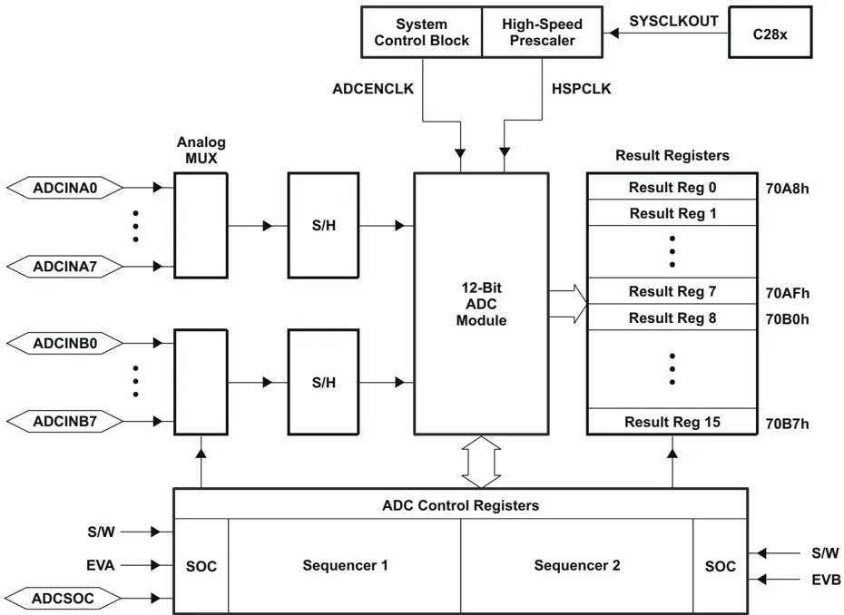
Figure 9-4. Block Diagram of the F281x ADC Module
To obtain the specified accuracy of the ADC, proper board layout is critical. To the best extent possible, traces leading to the ADCIN pins should not run in close proximity to the digital signal paths. This is to minimize switching noise on the digital lines from getting coupled to the ADC inputs. Furthermore, proper isolation techniques must be used to isolate the ADC module power pins (VDDA1/VDDA2, AVDDREFBG) from the digital supply. For better accuracy and ESD protection, unused ADC inputs should be connected to analog ground.
Notes:
- The ADC registers are accessed at the SYSCLKOUT rate. The internal timing of the ADC module is controlled by the high-speed peripheral clock (HSPCLK).
- The behavior of the ADC module based on the state of the ADCENCLK and HALT signals is as follows:
ADCENCLK: On reset, this signal will be low. While reset is active-low (XRS) the clock to the register will still function. This is necessary to make sure all registers and modes go into their default reset state. The analog module will, however, be in a low-power inactive state. As soon as reset goes high, then the clock to the registers will be disabled. When the user sets the ADCENCLK signal high, then the clocks to the registers will be enabled and the analog module will be enabled. There will be a certain time delay (ms range) before the ADC is stable and can be used.
HALT: This signal only affects the analog module. It does not affect the registers. If low, the ADC module is powered. If high, the ADC module goes into low-power mode. The HALT mode will stop the clock to the CPU, which will stop the HSPCLK. Therefore the ADC register logic will be turned off indirectly.
Figure 9-5 shows the ADC pin-biasing for internal reference and Figure 9-6 shows the ADC pin-biasing for external reference.
Copyright © 2021 Texas Instruments Incorporated Submit Document Feedback 103 Product Folder Links: TMS320F2810 TMS320F2810-Q1 TMS320F2811 TMS320F2811-Q1 TMS320F2812 TMS320F2812-Q1
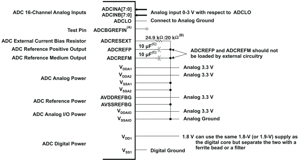
A. Provide access to this pin in PCB layouts. Intended for test purposes only. B. Use 24.9 kΩ for ADC clock range 1–18.75 MHz; use 20 kΩ for ADC clock range 18.75–25 MHz. C. TAIYO YUDEN EMK325F106ZH, EMK325BJ106MD, or equivalent ceramic capacitor D. External decoupling capacitors are recommended on all power pins. E. Analog inputs must be driven from an operational amplifier that does not degrade the ADC performance.
Figure 9-5. ADC Pin Connections With Internal Reference
Note
The temperature rating of any recommended component must match the rating of the end product.
TMS320F2810, TMS320F2810-Q1, TMS320F2811, TMS320F2811-Q1
TMS320F2812, TMS320F2812-Q1
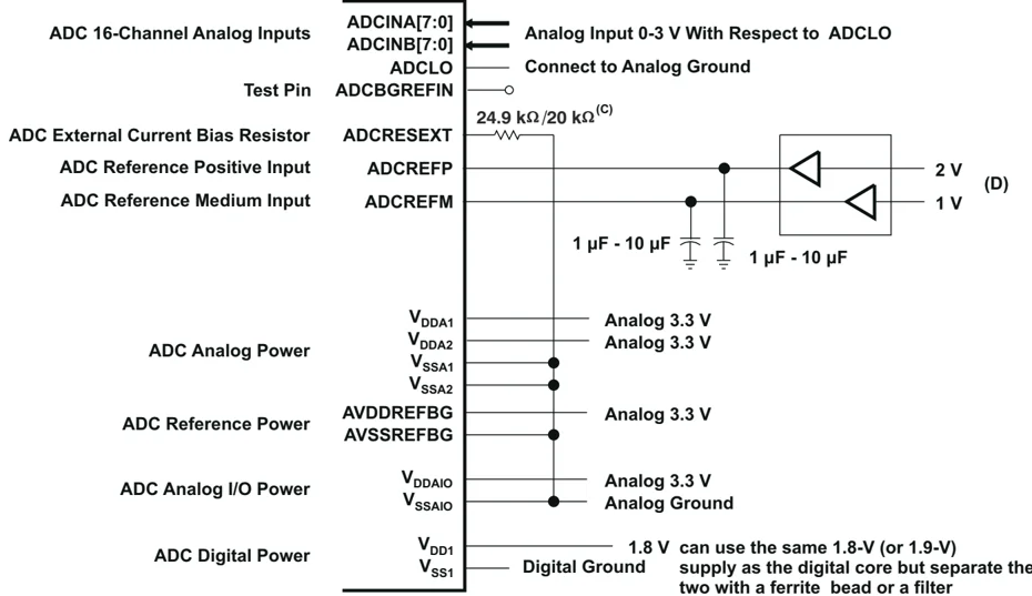
A. External decoupling capacitors are recommended on all power pins. B. Analog inputs must be driven from an operational amplifier that does not degrade the ADC performance. C. Use 24.9 kΩ for ADC clock range 1–18.75 MHz; use 20 kΩ for ADC clock range 18.75–25 MHz. D. It is recommended that buffered external references be provided with a voltage difference of (ADCREFP – ADCREFM) = 1 V ± 0.1% or better. External reference is enabled using bit 8 in the ADCTRL3 Register at ADC power up. In this mode, the accuracy of external reference is critical for overall gain. The voltage ADCREFP – ADCREFM will determine the overall accuracy. Do not enable internal references when external references are connected to ADCREFP and ADCREFM. See the TMS320x281x DSP Analog-to-Digital Converter (ADC) Reference Guide for more information.
Figure 9-6. ADC Pin Connections With External Reference
Submit Document Feedback 105
The ADC operation is configured, controlled, and monitored by the registers listed in Table 9-6.
Table 9-6. ADC Registers
| NAME(1) | ADDRESS | SIZE (x16) | DESCRIPTION |
|---|---|---|---|
| ADCTRL1 | 0x00 7100 | 1 | ADC Control Register 1 |
| ADCTRL2 | 0x00 7101 | 1 | ADC Control Register 2 |
| ADCMAXCONV | 0x00 7102 | 1 | ADC Maximum Conversion Channels Register |
| ADCCHSELSEQ1 | 0x00 7103 | 1 | ADC Channel Select Sequencing Control Register 1 |
| ADCCHSELSEQ2 | 0x00 7104 | 1 | ADC Channel Select Sequencing Control Register 2 |
| ADCCHSELSEQ3 | 0x00 7105 | 1 | ADC Channel Select Sequencing Control Register 3 |
| ADCCHSELSEQ4 | 0x00 7106 | 1 | ADC Channel Select Sequencing Control Register 4 |
| ADCASEQSR | 0x00 7107 | 1 | ADC Auto-Sequence Status Register |
| ADCRESULT0 | 0x00 7108 | 1 | ADC Conversion Result Buffer Register 0 |
| ADCRESULT1 | 0x00 7109 | 1 | ADC Conversion Result Buffer Register 1 |
| ADCRESULT2 | 0x00 710A | 1 | ADC Conversion Result Buffer Register 2 |
| ADCRESULT3 | 0x00 710B | 1 | ADC Conversion Result Buffer Register 3 |
| ADCRESULT4 | 0x00 710C | 1 | ADC Conversion Result Buffer Register 4 |
| ADCRESULT5 | 0x00 710D | 1 | ADC Conversion Result Buffer Register 5 |
| ADCRESULT6 | 0x00 710E | 1 | ADC Conversion Result Buffer Register 6 |
| ADCRESULT7 | 0x00 710F | 1 | ADC Conversion Result Buffer Register 7 |
| ADCRESULT8 | 0x00 7110 | 1 | ADC Conversion Result Buffer Register 8 |
| ADCRESULT9 | 0x00 7111 | 1 | ADC Conversion Result Buffer Register 9 |
| ADCRESULT10 | 0x00 7112 | 1 | ADC Conversion Result Buffer Register 10 |
| ADCRESULT11 | 0x00 7113 | 1 | ADC Conversion Result Buffer Register 11 |
| ADCRESULT12 | 0x00 7114 | 1 | ADC Conversion Result Buffer Register 12 |
| ADCRESULT13 | 0x00 7115 | 1 | ADC Conversion Result Buffer Register 13 |
| ADCRESULT14 | 0x00 7116 | 1 | ADC Conversion Result Buffer Register 14 |
| ADCRESULT15 | 0x00 7117 | 1 | ADC Conversion Result Buffer Register 15 |
| ADCTRL3 | 0x00 7118 | 1 | ADC Control Register 3 |
| ADCST | 0x00 7119 | 1 | ADC Status Register |
| Reserved | 0x00 711C – 0x00 711F | 4 |
(1) The above registers are Peripheral Frame 2 Registers.
9.2.4 Enhanced Controller Area Network (eCAN) Module
The CAN module has the following features:
- Fully compliant with ISO 11898-1 (CAN 2.0B)
- Supports data rates up to 1 Mbps
- Thirty-two mailboxes, each with the following properties:
- Configurable as receive or transmit
- Configurable with standard or extended identifier
- Has a programmable receive mask
- Supports data and remote frame
- Composed of 0 to 8 bytes of data
- Uses a 32-bit time stamp on receive and transmit message
- Protects against reception of new message
- Holds the dynamically programmable priority of transmit message
- Employs a programmable interrupt scheme with two interrupt levels
- Employs a programmable alarm on transmission or reception time-out
- Low-power mode
- Programmable wake-up on bus activity
- Automatic reply to a remote request message
- Automatic retransmission of a frame in case of loss of arbitration or error
- 32-bit local network time counter synchronized by a specific message (communication in conjunction with mailbox 16)
- Self-test mode
- Operates in a loopback mode receiving its own message. A “dummy” acknowledge is provided, thereby eliminating the need for another node to provide the acknowledge bit.
Note
NOTE: For a SYSCLKOUT of 150 MHz, the smallest bit rate possible is 23.4 kbps.
The 28x CAN has passed the conformance test per ISO/DIS 16845. Contact TI for details.
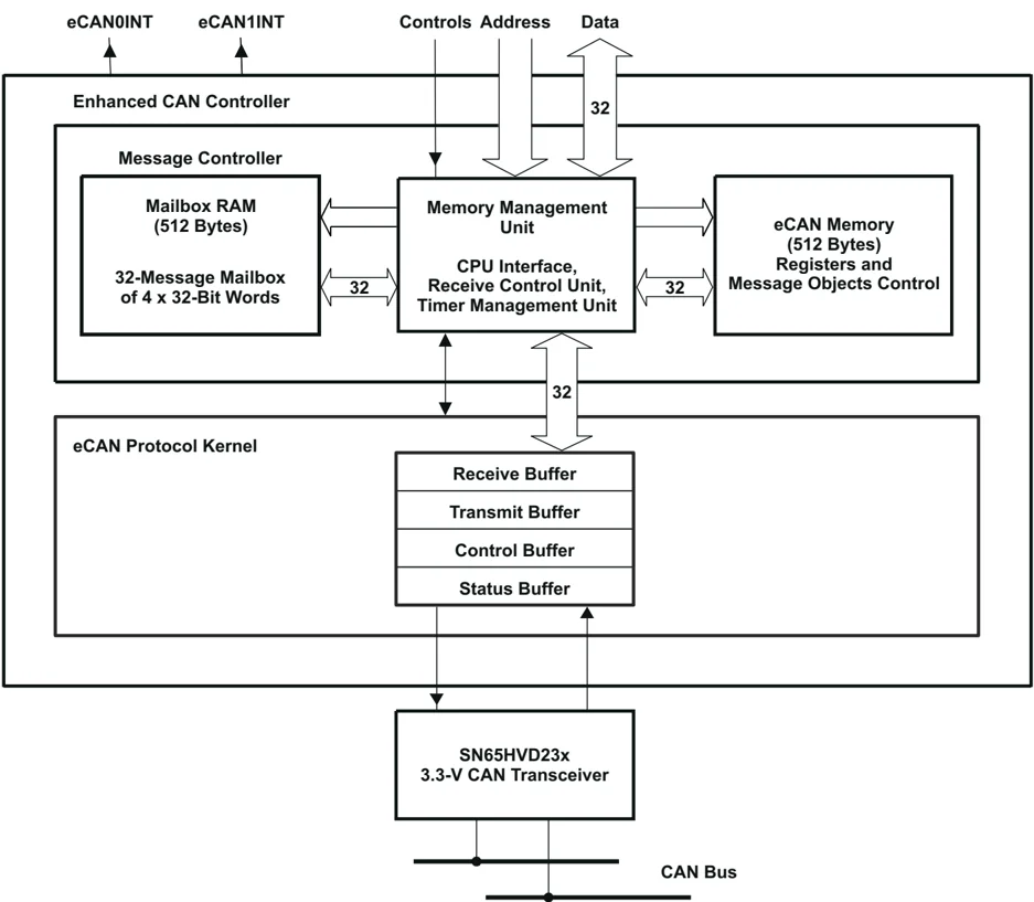
Figure 9-7. eCAN Block Diagram and Interface Circuit
108 Submit Document Feedback Copyright © 2021 Texas Instruments Incorporated Product Folder Links: TMS320F2810 TMS320F2810-Q1 TMS320F2811 TMS320F2811-Q1 TMS320F2812 TMS320F2812-Q1
Table 9-7. 3.3-V eCAN Transceivers for the TMS320F281x DSPs
| PART NUMBER | SUPPLY VOLTAGE | LOW-POWER MODE | SLOPE CONTROL | VREF | OTHER | TA |
|---|---|---|---|---|---|---|
| SN65HVD230 | 3.3 V | Standby | Adjustable | Yes | – | –40°C to 85°C |
| SN65HVD230Q | 3.3 V | Standby | Adjustable | Yes | – | –40°C to 125°C |
| SN65HVD231 | 3.3 V | Sleep | Adjustable | Yes | – | –40°C to 85°C |
| SN65HVD231Q | 3.3 V | Sleep | Adjustable | Yes | – | –40°C to 125°C |
| SN65HVD232 | 3.3 V | None | None | None | – | –40°C to 85°C |
| SN65HVD232Q | 3.3 V | None | None | None | – | –40°C to 125°C |
| SN65HVD233 | 3.3 V | Standby | Adjustable | None | Diagnostic Loopback | –40°C to 125°C |
| SN65HVD234 | 3.3 V | Standby and Sleep | Adjustable | None | – | –40°C to 125°C |
| SN65HVD235 | 3.3 V | Standby | Adjustable | None | Autobaud Loopback | –40°C to 125°C |
| ISO1050 | 3–5.5 V | None | None | None | Built-in IsolationLow Prop DelayThermal ShutdownFailsafe OperationDominant Time-out | –55°C to 105°C |
TEXAS INSTRUMENTS www.ti.com
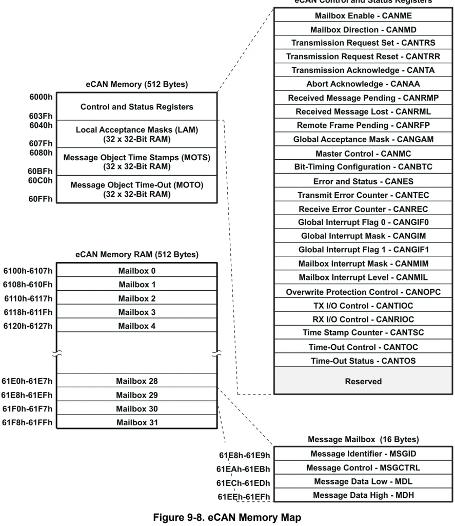
Figure 9-8. eCAN Memory Map
Note
If the eCAN module is not used in an application, the RAM available (LAM, MOTS, MOTO, and mailbox RAM) can be used as general-purpose RAM. The CAN module clock should be enabled for this.
Product Folder Links: TMS320F2810 TMS320F2810-Q1 TMS320F2811 TMS320F2811-Q1 TMS320F2812 TMS320F2812-Q1
TMS320F2810, TMS320F2810-Q1, TMS320F2811, TMS320F2811-Q1
TMS320F2812, TMS320F2812-Q1
The CAN registers listed in Table 9-8 are used by the CPU to configure and control the CAN controller and the message objects. eCAN control registers only support 32-bit read/write operations. Mailbox RAM can be accessed as 16 bits or 32 bits. 32-bit accesses are aligned to an even boundary.
Table 9-8. CAN Registers
| NAME(1) | ADDRESS | SIZE (x32) | DESCRIPTION |
|---|---|---|---|
| CANME | 0x00 6000 | 1 | Mailbox enable |
| CANMD | 0x00 6002 | 1 | Mailbox direction |
| CANTRS | 0x00 6004 | 1 | Transmit request set |
| CANTRR | 0x00 6006 | 1 | Transmit request reset |
| CANTA | 0x00 6008 | 1 | Transmission acknowledge |
| CANAA | 0x00 600A | 1 | Abort acknowledge |
| CANRMP | 0x00 600C | 1 | Receive message pending |
| CANRML | 0x00 600E | 1 | Receive message lost |
| CANRFP | 0x00 6010 | 1 | Remote frame pending |
| CANGAM | 0x00 6012 | 1 | Global acceptance mask |
| CANMC | 0x00 6014 | 1 | Master control |
| CANBTC | 0x00 6016 | 1 | Bit-timing configuration |
| CANES | 0x00 6018 | 1 | Error and status |
| CANTEC | 0x00 601A | 1 | Transmit error counter |
| CANREC | 0x00 601C | 1 | Receive error counter |
| CANGIF0 | 0x00 601E | 1 | Global interrupt flag 0 |
| CANGIM | 0x00 6020 | 1 | Global interrupt mask |
| CANGIF1 | 0x00 6022 | 1 | Global interrupt flag 1 |
| CANMIM | 0x00 6024 | 1 | Mailbox interrupt mask |
| CANMIL | 0x00 6026 | 1 | Mailbox interrupt level |
| CANOPC | 0x00 6028 | 1 | Overwrite protection control |
| CANTIOC | 0x00 602A | 1 | TX I/O control |
| CANRIOC | 0x00 602C | 1 | RX I/O control |
| CANTSC | 0x00 602E | 1 | Time stamp counter (Reserved in SCC mode) |
| CANTOC | 0x00 6030 | 1 | Time-out control (Reserved in SCC mode) |
| CANTOS | 0x00 6032 | 1 | Time-out status (Reserved in SCC mode) |
(1) These registers are mapped to Peripheral Frame 1.
Submit Document Feedback 111