9.2.5 Multichannel Buffered Serial Port (McBSP) Module
The McBSP module has the following features:
- Compatible to McBSP in TMS320C54x/TMS320C55x DSP devices, except the DMA features
- Full-duplex communication
- Double-buffered data registers which allow a continuous data stream
- Independent framing and clocking for receive and transmit
- External shift clock generation or an internal programmable frequency shift clock
- A wide selection of data sizes including 8-, 12-, 16-, 20-, 24-, or 32-bits
- 8-bit data transfers with LSB or MSB first
- Programmable polarity for both frame synchronization and data clocks
- Highly programmable internal clock and frame generation
- Support A-bis mode
- Direct interface to industry-standard CODECs, Analog Interface Chips (AICs), and other serially connected A/D and D/A devices
- Works with SPI-compatible devices
- Two 16 x 16-level FIFO for Transmit channel
- Two 16 x 16-level FIFO for Receive channel
The following application interfaces can be supported on the McBSP:
- T1/E1 framers
- MVIP switching-compatible and ST-BUS-compliant devices including:
- MVIP framers
- H.100 framers
- SCSA framers
- IOM-2 compliant devices
- AC97-compliant devices (the necessary multiphase frame synchronization capability is provided.)
- IIS-compliant devices
- McBSP clock rate = CLKG = CLKSRG/(1 + CLKGDIV), where CLKSRG source could be LSPCLK, CLKX, or CLKR.¹
¹ Serial port performance is limited by I/O buffer switching speed. Internal prescalers must be adjusted such that the peripheral speed is less than the I/O buffer speed limit—20-MHz maximum.
Texas INSTRUMENTS www.ti.com
TMS320F2812, TMS320F2812-Q1 SPRS174V – APRIL 2001 – REVISED FEBRUARY 2021
Figure 9-9 shows the block diagram of the McBSP module with FIFO, interfaced to the F281x version of Peripheral Frame 2.

Figure 9-9. McBSP Module With FIFO
Submit Document Feedback 113 Product Folder Links: TMS320F2810 TMS320F2810-Q1 TMS320F2811 TMS320F2811-Q1 TMS320F2812 TMS320F2812-Q1
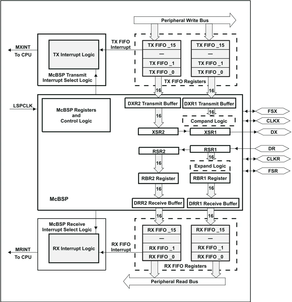
Table 9-9 provides a summary of the McBSP registers.
Table 9-9. McBSP Registers
| NAME | ADDRESS 0x00 78xxh | TYPE (R/W) | RESET VALUE (HEX) | DESCRIPTION |
|---|---|---|---|---|
| DATA REGISTERS, RECEIVE, TRANSMIT (1) | ||||
| – | – | – | 0x0000 | McBSP Receive Buffer Register |
| – | – | – | 0x0000 | McBSP Receive Shift Register |
| – | – | – | 0x0000 | McBSP Transmit Shift Register |
| DRR2 | 00 | R | 0x0000 | McBSP Data Receive Register 2• Read First if the word size is greater than 16 bits, else ignore DRR2 |
| DRR1 | 01 | R | 0x0000 | McBSP Data Receive Register 1• Read Second if the word size is greater than 16 bits, else read DRR1 only |
| DXR2 | 02 | W | 0x0000 | McBSP Data Transmit Register 2• Write First if the word size is greater than 16 bits, else ignore DXR2 |
| DXR1 | 03 | W | 0x0000 | McBSP Data Transmit Register 1• Write Second if the word size is greater than 16 bits, else write to DXR1 only |
| McBSP CONTROL REGISTERS | ||||
| SPCR2 | 04 | R/W | 0x0000 | McBSP Serial Port Control Register 2 |
| SPCR1 | 05 | R/W | 0x0000 | McBSP Serial Port Control Register 1 |
| RCR2 | 06 | R/W | 0x0000 | McBSP Receive Control Register 2 |
| RCR1 | 07 | R/W | 0x0000 | McBSP Receive Control Register 1 |
| XCR2 | 08 | R/W | 0x0000 | McBSP Transmit Control Register 2 |
| XCR1 | 09 | R/W | 0x0000 | McBSP Transmit Control Register 1 |
| SRGR2 | 0A | R/W | 0x0000 | McBSP Sample Rate Generator Register 2 |
| SRGR1 | 0B | R/W | 0x0000 | McBSP Sample Rate Generator Register 1 |
| MULTICHANNEL CONTROL REGISTERS | ||||
| MCR2 | 0C | R/W | 0x0000 | McBSP Multichannel Register 2 |
| MCR1 | 0D | R/W | 0x0000 | McBSP Multichannel Register 1 |
| RCERA | 0E | R/W | 0x0000 | McBSP Receive Channel Enable Register Partition A |
| RCERB | 0F | R/W | 0x0000 | McBSP Receive Channel Enable Register Partition B |
| XCERA | 10 | R/W | 0x0000 | McBSP Transmit Channel Enable Register Partition A |
| XCERB | 11 | R/W | 0x0000 | McBSP Transmit Channel Enable Register Partition B |
| PCR | 12 | R/W | 0x0000 | McBSP Pin Control Register |
| RCERC | 13 | R/W | 0x0000 | McBSP Receive Channel Enable Register Partition C |
| RCERD | 14 | R/W | 0x0000 | McBSP Receive Channel Enable Register Partition D |
| XCERC | 15 | R/W | 0x0000 | McBSP Transmit Channel Enable Register Partition C |
| XCERD | 16 | R/W | 0x0000 | McBSP Transmit Channel Enable Register Partition D |
| RCERE | 17 | R/W | 0x0000 | McBSP Receive Channel Enable Register Partition E |
| RCERF | 18 | R/W | 0x0000 | McBSP Receive Channel Enable Register Partition F |
| XCERE | 19 | R/W | 0x0000 | McBSP Transmit Channel Enable Register Partition E |
| XCERF | 1A | R/W | 0x0000 | McBSP Transmit Channel Enable Register Partition F |
| RCERG | 1B | R/W | 0x0000 | McBSP Receive Channel Enable Register Partition G |
| RCERH | 1C | R/W | 0x0000 | McBSP Receive Channel Enable Register Partition H |
| XCERG | 1D | R/W | 0x0000 | McBSP Transmit Channel Enable Register Partition G |
TMS320F2810, TMS320F2810-Q1, TMS320F2811, TMS320F2811-Q1
TMS320F2812, TMS320F2812-Q1
Table 9-9. McBSP Registers (continued)
| NAME | ADDRESS 0x00 78xxh | TYPE (R/W) | RESET VALUE (HEX) | DESCRIPTION |
|---|---|---|---|---|
| XCERH | 1E | R/W | 0x0000 | McBSP Transmit Channel Enable Register Partition H |
Submit Document Feedback 115
Table 9-9. McBSP Registers (continued)
| NAME | ADDRESS 0x00 78xxh | TYPE (R/W) | RESET VALUE (HEX) | DESCRIPTION |
|---|---|---|---|---|
| FIFO MODE REGISTERS (applicable only in FIFO mode) | ||||
| FIFO Data Registers (2) | ||||
| DRR2 | 00 | R | 0x0000 | McBSP Data Receive Register 2 – Top of receive FIFO• Read First FIFO pointers will not advance |
| DRR1 | 01 | R | 0x0000 | McBSP Data Receive Register 1 – Top of receive FIFO• Read Second for FIFO pointers to advance |
| DXR2 | 02 | W | 0x0000 | McBSP Data Transmit Register 2 – Top of transmit FIFO• Write First FIFO pointers will not advance |
| DXR1 | 03 | W | 0x0000 | McBSP Data Transmit Register 1 – Top of transmit FIFO• Write Second for FIFO pointers to advance |
| FIFO Control Registers | ||||
| MFFTX | 20 | R/W | 0xA000 | McBSP Transmit FIFO Register |
| MFFRX | 21 | R/W | 0x201F | McBSP Receive FIFO Register |
| MFFCT | 22 | R/W | 0x0000 | McBSP FIFO Control Register |
| MFFINT | 23 | R/W | 0x0000 | McBSP FIFO Interrupt Register |
| MFFST | 24 | R/W | 0x0000 | McBSP FIFO Status Register |
(1) DRR2/DRR1 and DXR2/DXR1 share the same addresses of receive and transmit FIFO registers in FIFO mode.
(2) FIFO pointers advancing is based on order of access to DRR2/DRR1 and DXR2/DXR1 registers.
9.2.6 Serial Communications Interface (SCI) Module
The F281x devices include two serial communications interface (SCI) modules. The SCI modules support digital communications between the CPU and other asynchronous peripherals that use the standard non-return-to-zero (NRZ) format. The SCI receiver and transmitter are double-buffered, and each has its own separate enable and interrupt bits. Both can be operated independently or simultaneously in the full-duplex mode. To ensure data integrity, the SCI checks received data for break detection, parity, overrun, and framing errors. The bit rate is programmable to over 65000 different speeds through a 16-bit baud-select register.
Features of each SCI module include:
- Two external pins:
- SCITXD: SCI transmit-output pin
- SCIRXD: SCI receive-input pin
NOTE: Both pins can be used as GPIO if not used for SCI.
-
Baud rate programmable to 64K different rates²
$$ \text{Baud rate} = \frac{\text{LSPCLK}}{(\text{BRR} + 1) * 8} \quad \text{when BRR} \neq 0 $$
$$ = \frac{\text{LSPCLK}}{16} \quad \text{when BRR} = 0 $$
-
Data-word format
- One start bit
- Data-word length programmable from one to eight bits
- Optional even/odd/no parity bit
- One or two stop bits
-
Four error-detection flags: parity, overrun, framing, and break detection
-
Two wake-up multiprocessor modes: idle-line and address bit
-
Half- or full-duplex operation
-
Double-buffered receive and transmit functions
-
Transmitter and receiver operations can be accomplished through interrupt-driven or polled algorithms with status flags.
- Transmitter: TXRDY flag (transmitter-buffer register is ready to receive another character) and TX EMPTY flag (transmitter-shift register is empty)
- Receiver: RXRDY flag (receiver-buffer register is ready to receive another character), BRKDT flag (break condition occurred), and RX ERROR flag (monitoring four interrupt conditions)
-
Separate enable bits for transmitter and receiver interrupts (except BRKDT)
-
Max bit rate = 75 MHz/16 = 4.688 x 10⁶ b/s
-
NRZ (non-return-to-zero) format
-
Ten SCI module control registers located in the control register frame beginning at address 7050h
NOTE: All registers in this module are 8-bit registers that are connected to Peripheral Frame 2. When a register is accessed, the register data is in the lower byte (7–0), and the upper byte (15–8) is read as zeros. Writing to the upper byte has no effect.
Enhanced features:
- Auto baud-detect hardware logic
- 16-level transmit/receive FIFO
² Serial port performance is limited by I/O buffer switching speed. Internal prescalers must be adjusted such that the peripheral speed is less than the I/O buffer speed limit—20 MHz maximum.

The SCI port operation is configured and controlled by the registers listed in Table 9-10 and Table 9-11.
Table 9-10. SCI-A Registers
| NAME | ADDRESS | SIZE (x16) | DESCRIPTION |
|---|---|---|---|
| SCICCR A | 0x00 7050 | 1 | SCI-A Communications Control Register |
| SCICTL1A | 0x00 7051 | 1 | SCI-A Control Register 1 |
| SCIHBAUDA | 0x00 7052 | 1 | SCI-A Baud Register, High Bits |
| SCILBAUDA | 0x00 7053 | 1 | SCI-A Baud Register, Low Bits |
| SCICTL2A | 0x00 7054 | 1 | SCI-A Control Register 2 |
| SCIRXSTA | 0x00 7055 | 1 | SCI-A Receive Status Register |
| SCIRXEMU A | 0x00 7056 | 1 | SCI-A Receive Emulation Data Buffer Register |
| SCIRXBUFA | 0x00 7057 | 1 | SCI-A Receive Data Buffer Register |
| SCITXBUFA | 0x00 7059 | 1 | SCI-A Transmit Data Buffer Register |
| SCIFFTXA(1) | 0x00 705A | 1 | SCI-A FIFO Transmit Register |
| SCIFFRXA(1) | 0x00 705B | 1 | SCI-A FIFO Receive Register |
| SCIFFCTA(1) | 0x00 705C | 1 | SCI-A FIFO Control Register |
| SCIPRIA | 0x00 705F | 1 | SCI-A Priority Control Register |
(1) These registers are new registers for the FIFO mode.
Table 9-11. SCI-B Registers
| NAME | ADDRESS | SIZE (x16) | DESCRIPTION |
|---|---|---|---|
| SCICCRB | 0x00 7750 | 1 | SCI-B Communications Control Register |
| SCICTL1B | 0x00 7751 | 1 | SCI-B Control Register 1 |
| SCIHBAUDB | 0x00 7752 | 1 | SCI-B Baud Register, High Bits |
| SCILBAUDB | 0x00 7753 | 1 | SCI-B Baud Register, Low Bits |
| SCICTL2B | 0x00 7754 | 1 | SCI-B Control Register 2 |
| SCIRXSTB | 0x00 7755 | 1 | SCI-B Receive Status Register |
| SCIRXEMUB | 0x00 7756 | 1 | SCI-B Receive Emulation Data Buffer Register |
| SCIRXBUFB | 0x00 7757 | 1 | SCI-B Receive Data Buffer Register |
| SCITXBUFB | 0x00 7759 | 1 | SCI-B Transmit Data Buffer Register |
| SCIFFTXB(2) | 0x00 775A | 1 | SCI-B FIFO Transmit Register |
| SCIFFRXB(2) | 0x00 775B | 1 | SCI-B FIFO Receive Register |
| SCIFFCTB(2) | 0x00 775C | 1 | SCI-B FIFO Control Register |
| SCIPRIB | 0x00 775F | 1 | SCI-B Priority Control Register |
(1) Registers in this table are mapped to peripheral bus 16 space. This space only allows 16-bit accesses. 32-bit accesses produce undefined results.
(2) These registers are new registers for the FIFO mode.
Figure 9-10 shows the SCI module block diagram.
TEXAS INSTRUMENTS www.ti.com
SPRS174V – APRIL 2001 – REVISED FEBRUARY 2021
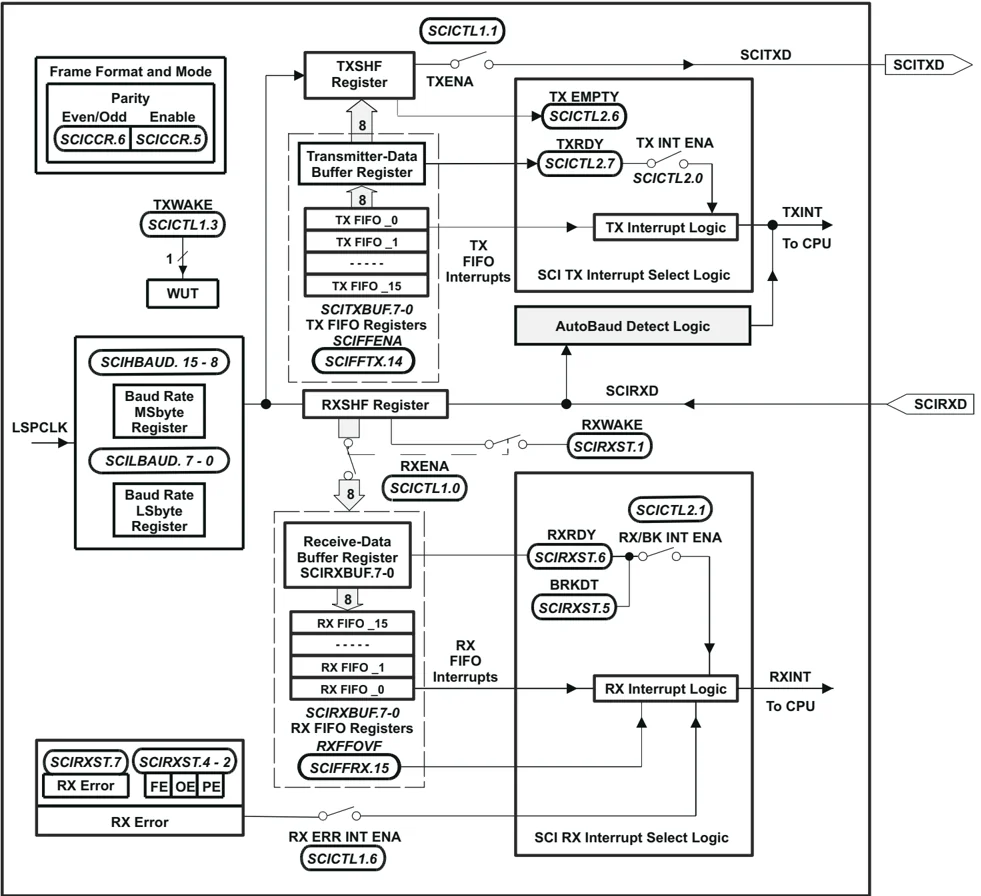
Figure 9-10. Serial Communications Interface (SCI) Module Block Diagram
Submit Document Feedback 119 Product Folder Links: TMS320F2810 TMS320F2810-Q1 TMS320F2811 TMS320F2811-Q1 TMS320F2812 TMS320F2812-Q1
9.2.7 Serial Peripheral Interface (SPI) Module
The F281x devices include the four-pin serial peripheral interface (SPI) module. The SPI is a high-speed, synchronous serial I/O port that allows a serial bit stream of programmed length (one to sixteen bits) to be shifted into and out of the device at a programmable bit-transfer rate. Normally, the SPI is used for communications between the DSP controller and external peripherals or another processor. Typical applications include external I/O or peripheral expansion through devices such as shift registers, display drivers, and ADCs. Multidevice communications are supported by the master/slave operation of the SPI.
The SPI module features include:
- Four external pins:
- SPISOMI: SPI slave-output/master-input pin
- SPISIMO: SPI slave-input/master-output pin
- SPISTE: SPI slave transmit-enable pin
- SPICLK: SPI serial-clock pin
NOTE: All four pins can be used as GPIO, if the SPI module is not used.
-
Two operational modes: master and slave
-
Baud rate: 125 different programmable rates
Baud rate = \fracLSPCLK(SPIBRR + 1) when SPIBRR ≠ 0
= \fracLSPCLK4 when SPIBRR = 0, 1, 2, 3
Serial port performance is limited by I/O buffer switching speed. Internal prescalers must be adjusted such that the peripheral speed is less than the I/O buffer speed limit—20 MHz maximum.
- Data word length: one to sixteen data bits
- Four clocking schemes (controlled by clock polarity and clock phase bits) include:
- Falling edge without phase delay: SPICLK active-high. SPI transmits data on the falling edge of the SPICLK signal and receives data on the rising edge of the SPICLK signal.
- Falling edge with phase delay: SPICLK active-high. SPI transmits data one half-cycle ahead of the falling edge of the SPICLK signal and receives data on the falling edge of the SPICLK signal.
- Rising edge without phase delay: SPICLK inactive-low. SPI transmits data on the rising edge of the SPICLK signal and receives data on the falling edge of the SPICLK signal.
- Rising edge with phase delay: SPICLK inactive-low. SPI transmits data one half-cycle ahead of the rising edge of the SPICLK signal and receives data on the rising edge of the SPICLK signal.
- Simultaneous receive and transmit operation (transmit function can be disabled in software)
- Transmitter and receiver operations are accomplished through either interrupt-driven or polled algorithms.
- Nine SPI module control registers: Located in control register frame beginning at address 7040h.
NOTE: All registers in this module are 16-bit registers that are connected to Peripheral Frame 2. When a register is accessed, the register data is in the lower byte (7–0), and the upper byte (15–8) is read as zeros. Writing to the upper byte has no effect.
Enhanced features:
- 16-level transmit/receive FIFO
- Delayed transmit control

The SPI port operation is configured and controlled by the registers listed in Table 9-12.
Table 9-12. SPI Registers
| NAME(1) | ADDRESS | SIZE (x16) | DESCRIPTION |
|---|---|---|---|
| SPICCR | 0x00 7040 | 1 | SPI Configuration Control Register |
| SPICTL | 0x00 7041 | 1 | SPI Operation Control Register |
| SPISTS | 0x00 7042 | 1 | SPI Status Register |
| SPIBRR | 0x00 7044 | 1 | SPI Baud Rate Register |
| SPIRXEMU | 0x00 7046 | 1 | SPI Receive Emulation Buffer Register |
| SPIRXBUF | 0x00 7047 | 1 | SPI Serial Input Buffer Register |
| SPITXBUF | 0x00 7048 | 1 | SPI Serial Output Buffer Register |
| SPIDAT | 0x00 7049 | 1 | SPI Serial Data Register |
| SPIFFTX | 0x00 704A | 1 | SPI FIFO Transmit Register |
| SPIFFRX | 0x00 704B | 1 | SPI FIFO Receive Register |
| SPIFFCT | 0x00 704C | 1 | SPI FIFO Control Register |
| SPIPRI | 0x00 704F | 1 | SPI Priority Control Register |
(1) These registers are mapped to Peripheral Frame 2. This space only allows 16-bit accesses. 32-bit accesses produce undefined results.
Figure 9-11 is a block diagram of the SPI in slave mode.
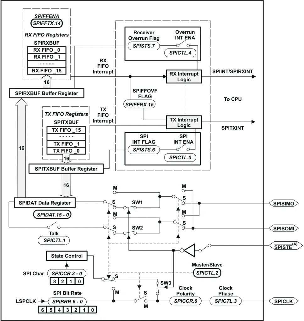
A. \overlineSPISTE is driven low by the master for a slave device.
Figure 9-11. Serial Peripheral Interface Module Block Diagram (Slave Mode)
122 Submit Document Feedback Copyright © 2021 Texas Instruments Incorporated Product Folder Links: TMS320F2810 TMS320F2810-Q1 TMS320F2811 TMS320F2811-Q1 TMS320F2812 TMS320F2812-Q1
9.2.8 GPIO MUX
The GPIO Mux registers are used to select the operation of shared pins on the F281x devices. The pins can be individually selected to operate as “Digital I/O” or connected to “Peripheral I/O” signals (via the GPxMUX registers). If selected for “Digital I/O”mode, registers are provided to configure the pin direction (via the GPxDIR registers) and to qualify the input signal to remove unwanted noise (via the GPxQUAL) registers). Table 9-13 lists the GPIO Mux Registers.
Table 9-13. GPIO Mux Registers
| NAME(1) (2) (3) | ADDRESS | SIZE (x16) | DESCRIPTION |
|---|---|---|---|
| GPAMUX | 0x00 70C0 | 1 | GPIO A Mux Control Register |
| GPADIR | 0x00 70C1 | 1 | GPIO A Direction Control Register |
| GPAQUAL | 0x00 70C2 | 1 | GPIO A Input Qualification Control Register |
| Reserved | 0x00 70C3 | 1 | |
| GPBMUX | 0x00 70C4 | 1 | GPIO B Mux Control Register |
| GPBDIR | 0x00 70C5 | 1 | GPIO B Direction Control Register |
| GPBQUAL | 0x00 70C6 | 1 | GPIO B Input Qualification Control Register |
| Reserved | 0x00 70C7 | 1 | |
| Reserved | 0x00 70C8 | 1 | |
| Reserved | 0x00 70C9 | 1 | |
| Reserved | 0x00 70CA | 1 | |
| Reserved | 0x00 70CB | 1 | |
| GPDMUX | 0x00 70CC | 1 | GPIO D Mux Control Register |
| GPDDIR | 0x00 70CD | 1 | GPIO D Direction Control Register |
| GPDQUAL | 0x00 70CE | 1 | GPIO D Input Qualification Control Register |
| Reserved | 0x00 70CF | 1 | |
| GPEMUX | 0x00 70D0 | 1 | GPIO E Mux Control Register |
| GPEDIR | 0x00 70D1 | 1 | GPIO E Direction Control Register |
| GPEQUAL | 0x00 70D2 | 1 | GPIO E Input Qualification Control Register |
| Reserved | 0x00 70D3 | 1 | |
| GPFMUX | 0x00 70D4 | 1 | GPIO F Mux Control Register |
| GPFDIR | 0x00 70D5 | 1 | GPIO F Direction Control Register |
| Reserved | 0x00 70D6 | 1 | |
| Reserved | 0x00 70D7 | 1 | |
| GPGMUX | 0x00 70D8 | 1 | GPIO G Mux Control Register |
| GPGDIR | 0x00 70D9 | 1 | GPIO G Direction Control Register |
| Reserved | 0x00 70DA | 1 | |
| Reserved | 0x00 70DB | 1 | |
| Reserved | 0x00 70DC – 0x00 70DF | 4 |
(1) Reserved locations return undefined values and writes are ignored. (2) Not all inputs support input signal qualification. (3) These registers are EALLOW protected. This prevents spurious writes from overwriting the contents and corrupting the system.

If configured for "Digital I/O" mode, additional registers are provided for setting individual I/O signals (via the GPxSET registers), for clearing individual I/O signals (via the GPxCLEAR registers), for toggling individual I/O signals (via the GPxTOGGLE registers), or for reading/writing to the individual I/O signals (via the GPxDAT registers). Table 9-14 lists the GPIO Data Registers. For more information, see the TMS320x281x DSP System Control and Interrupts Reference Guide.
Table 9-14. GPIO Data Registers
| NAME(1) (2) | ADDRESS | SIZE (x16) | DESCRIPTION |
|---|---|---|---|
| GPADAT | 0x00 70E0 | 1 | GPIO A Data Register |
| GPASET | 0x00 70E1 | 1 | GPIO A Set Register |
| GPACLEAR | 0x00 70E2 | 1 | GPIO A Clear Register |
| GPATOGGLE | 0x00 70E3 | 1 | GPIO A Toggle Register |
| GPBDAT | 0x00 70E4 | 1 | GPIO B Data Register |
| GPBSET | 0x00 70E5 | 1 | GPIO B Set Register |
| GPBCLEAR | 0x00 70E6 | 1 | GPIO B Clear Register |
| GPBTOGGLE | 0x00 70E7 | 1 | GPIO B Toggle Register |
| Reserved | 0x00 70E8 | 1 | |
| Reserved | 0x00 70E9 | 1 | |
| Reserved | 0x00 70EA | 1 | |
| Reserved | 0x00 70EB | 1 | |
| GPDDAT | 0x00 70EC | 1 | GPIO D Data Register |
| GPDSET | 0x00 70ED | 1 | GPIO D Set Register |
| GPDCLEAR | 0x00 70EE | 1 | GPIO D Clear Register |
| GPDTOGGLE | 0x00 70EF | 1 | GPIO D Toggle Register |
| GPEDAT | 0x00 70F0 | 1 | GPIO E Data Register |
| GPESET | 0x00 70F1 | 1 | GPIO E Set Register |
| GPECLEAR | 0x00 70F2 | 1 | GPIO E Clear Register |
| GPETOGGLE | 0x00 70F3 | 1 | GPIO E Toggle Register |
| GPFDAT | 0x00 70F4 | 1 | GPIO F Data Register |
| GPFSET | 0x00 70F5 | 1 | GPIO F Set Register |
| GPFCLEAR | 0x00 70F6 | 1 | GPIO F Clear Register |
| GPFTOGGLE | 0x00 70F7 | 1 | GPIO F Toggle Register |
| GPGDAT | 0x00 70F8 | 1 | GPIO G Data Register |
| GPGSET | 0x00 70F9 | 1 | GPIO G Set Register |
| GPGCLEAR | 0x00 70FA | 1 | GPIO G Clear Register |
| GPGTOGGLE | 0x00 70FB | 1 | GPIO G Toggle Register |
| Reserved | 0x00 70FC – 0x00 70FF | 4 |
(1) Reserved locations will return undefined values and writes will be ignored. (2) These registers are NOT EALLOW protected. The above registers will typically be accessed regularly by the user.
TMS320F2810, TMS320F2810-Q1, TMS320F2811, TMS320F2811-Q1
TMS320F2812, TMS320F2812-Q1
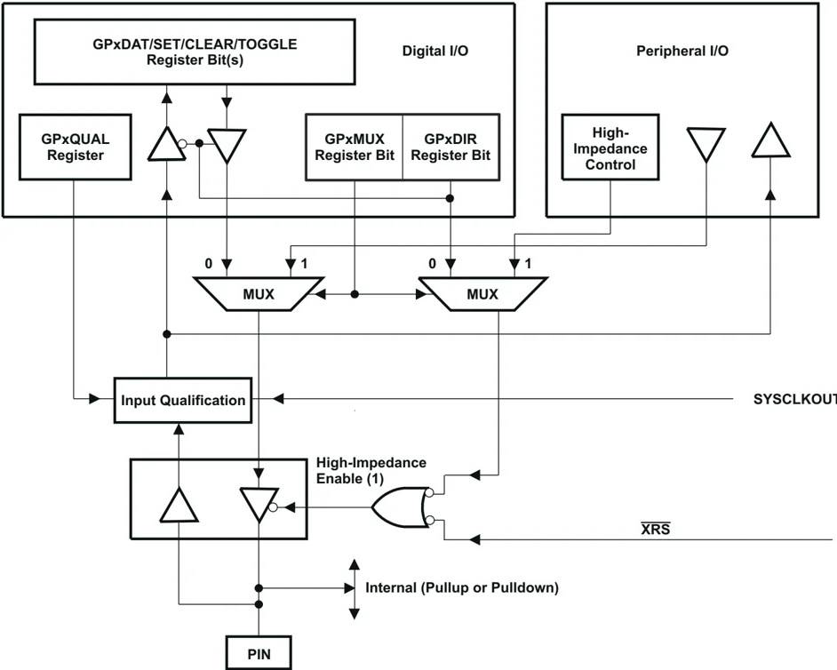
Figure 9-12 shows how the various register bits select the various modes of operation for GPIO function.

A. In the GPIO mode, when the GPIO pin is configured for output operation, reading the GPxDAT data register only gives the value written, not the value at the pin. In the peripheral mode, the state of the pin can be read through the GPxDAT register, provided the corresponding direction bit is zero (input mode).
B. Some selected input signals are qualified by the SYSCLKOUT. The GPxQUAL register specifies the qualification sampling period. The sampling window is 6 samples wide and the output is only changed when all samples are the same (all 0's or all 1's). This feature removes unwanted spikes from the input signal.
Figure 9-12. GPIO/Peripheral Pin Multiplexing
Note
The input function of the GPIO pin and the input path to the peripheral are always enabled. It is the output function of the GPIO pin that is multiplexed with the output path of the primary (peripheral) function. Since the output buffer of a pin connects back to the input buffer, any GPIO signal present at the pin will be propagated to the peripheral module as well. Therefore, when a pin is configured for GPIO operation, the corresponding peripheral functionality (and interrupt-generating capability) must be disabled. Otherwise, interrupts may be inadvertently triggered. This is especially critical when the PDPINTA and PDPINTB pins are used as GPIO pins, since a value of zero for GPDDAT.0 or GPDDAT.5 (PDPINTx) will put PWM pins in a high-impedance state. The CxTRIP and TxCTTRIP pins will also put the corresponding PWM pins in high impedance, if they are driven low (as GPIO pins) and bit EXTCONx.0 = 1.
Submit Document Feedback 125
TMS320F2810, TMS320F2810-Q1, TMS320F2811, TMS320F2811-Q1
9.3 Memory Maps
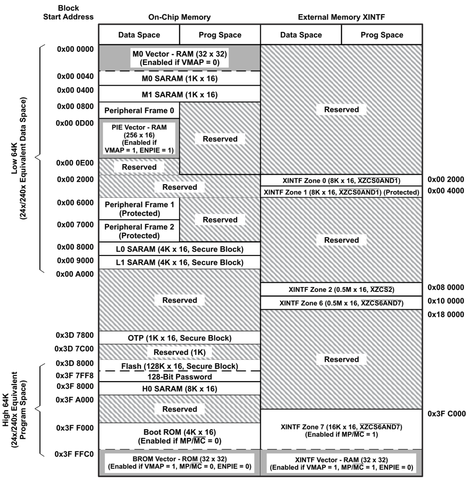
LEGEND:
Only one of these vector maps - M0 vector, PIE vector, BROM vector, XINTF vector - should be enabled at a time.
A. Memory blocks are not to scale. B. Reserved locations are reserved for future expansion. Application should not access these areas. C. Boot ROM and Zone 7 memory maps are active either in on-chip or XINTF zone depending on MP/MC, not in both. D. Peripheral Frame 0, Peripheral Frame 1, and Peripheral Frame 2 memory maps are restricted to data memory only. User program cannot access these memory maps in program space. E. "Protected" means the order of Write followed by Read operations is preserved rather than the pipeline order. F. Certain memory ranges are EALLOW protected against spurious writes after configuration. G. Zones 0 and 1 and Zones 6 and 7 share the same chip select; hence, these memory blocks have mirrored locations.
Figure 9-13. F2812 Memory Map
126 Submit Document Feedback Copyright © 2021 Texas Instruments Incorporated Product Folder Links: TMS320F2810 TMS320F2810-Q1 TMS320F2811 TMS320F2811-Q1 TMS320F2812 TMS320F2812-Q1
TEXAS INSTRUMENTS www.ti.com
SPRS174V – APRIL 2001 – REVISED FEBRUARY 2021
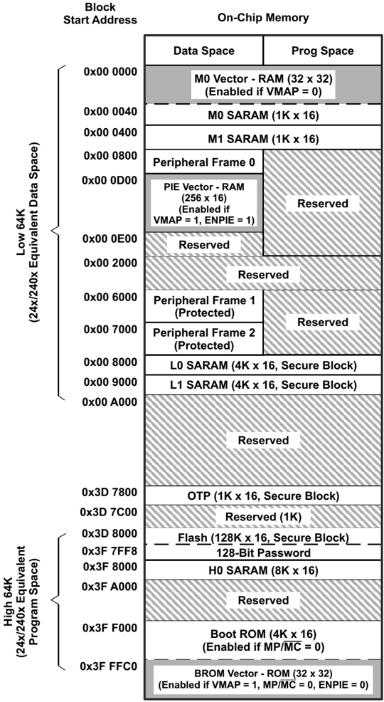
LEGEND: Only one of these vector maps - M0 vector, PIE vector, BROM vector - should be enabled at a time.
A. Memory blocks are not to scale. B. Reserved locations are reserved for future expansion. Application should not access these areas. C. Peripheral Frame 0, Peripheral Frame 1, and Peripheral Frame 2 memory maps are restricted to data memory only. User program cannot access these memory maps in program space. D. "Protected" means the order of Write followed by Read operations is preserved rather than the pipeline order. E. Certain memory ranges are EALLOW protected against spurious writes after configuration.
Figure 9-14. F2811 Memory Map
Submit Document Feedback 127 Product Folder Links: TMS320F2810 TMS320F2810-Q1 TMS320F2811 TMS320F2811-Q1 TMS320F2812 TMS320F2812-Q1
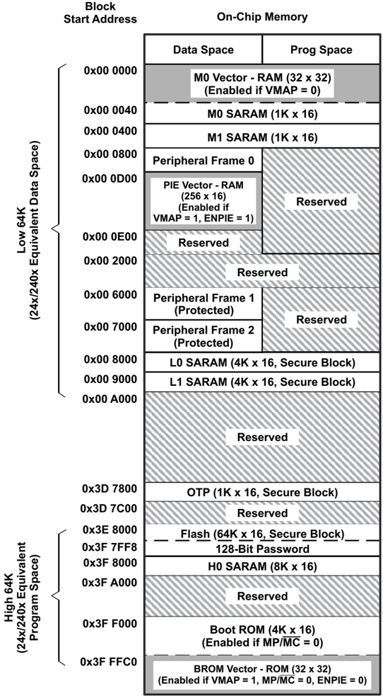
LEGEND:
Only one of these vector maps - M0 vector, PIE vector, BROM vector - should be enabled at a time.
A. Memory blocks are not to scale.
B. Reserved locations are reserved for future expansion. Application should not access these areas.
C. Peripheral Frame 0, Peripheral Frame 1, and Peripheral Frame 2 memory maps are restricted to data memory only. User program cannot access these memory maps in program space.
D. “Protected” means the order of Write followed by Read operations is preserved rather than the pipeline order.
E. Certain memory ranges are EALLOW protected against spurious writes after configuration.
Figure 9-15. F2810 Memory Map
Table 9-15. Addresses of Flash Sectors in F2812 and F2811
| ADDRESS RANGE | PROGRAM AND DATA SPACE |
|---|---|
| 0x3D 80000x3D 9FFF | Sector J, 8K x 16 |
| 0x3D A0000x3D BFFF | Sector I, 8K x 16 |
| 0x3D C0000x3D FFFF | Sector H, 16K x 16 |
| 0x3E 00000x3E 3FFF | Sector G, 16K x 16 |
| 0x3E 40000x3E 7FFF | Sector F, 16K x 16 |
| 0x3E 80000x3E BFFF | Sector E, 16K x 16 |
| 0x3E C0000x3E FFFF | Sector D, 16K x 16 |
| 0x3F 00000x3F 3FFF | Sector C, 16K x 16 |
| 0x3F 40000x3F 5FFF | Sector B, 8K x 16 |
| 0x3F 6000 0x3F 7F800x3F 7FF5 0x3F 7FF60x3F 7FF7 0x3F 7FF80x3F 7FFF | Sector A, 8K x 16 Program to 0x0000 when using theCode Security Module Boot-to-Flash Entry Point(program branch instruction here) SecurityPassword (128-Bit)(Do not program to all zeros) |
Table 9-16. Addresses of Flash Sectors in F2810
| ADDRESS RANGE | PROGRAM AND DATA SPACE |
|---|---|
| 0x3E 80000x3E BFFF | Sector E, 16K x 16 |
| 0x3E C0000x3E FFFF | Sector D, 16K x 16 |
| 0x3F 00000x3F 3FFF | Sector C, 16K x 16 |
| 0x3F 40000x3F 5FFF | Sector B, 8K x 16 |
| 0x3F 6000 0x3F 7F800x3F 7FF5 0x3F 7FF60x3F 7FF7 0x3F 7FF80x3F 7FFF | Sector A, 8K x 16 Program to 0x0000 when using theCode Security Module Boot-to-Flash Entry Point(program branch instruction here) SecurityPassword (128-Bit)(Do not program to all zeros) |
The “Low 64K” of the memory address range maps into the data space of the 240x. The “High 64K” of the memory address range maps into the program space of the 24x/240x. 24x/240x-compatible code will execute only from the “High 64K”memory area. Hence, the top 32K of Flash and H0 SRAM block can be used to run 24x/240x-compatible code (if MP/ \overlineMC mode is low) or, on the F2812, code can be executed from XINTF Zone 7 (if MP/ \overlineMC mode is high).
The XINTF consists of five independent zones. One zone has its own chip select and the remaining four zones share two chip selects. Each zone can be programmed with its own timing (wait states) and to either sample or ignore external ready signal. This makes interfacing to external peripherals easy and glueless.

Note
The chip selects of XINTF Zone 0 and Zone 1 are merged into a single chip select (XZCS0AND1); and the chip selects of XINTF Zone 6 and Zone 7 are merged into a single chip select (XZCS6AND7). See Section 9.6, External Interface, XINTF (F2812 only), for details.
Peripheral Frame 1, Peripheral Frame 2, and XINTF Zone 1 are grouped together to enable these blocks to be “write/read peripheral block protected”. The “protected” mode ensures that all accesses to these blocks happen as written. Because of the C28x pipeline, a write immediately followed by a read, to different memory locations, will appear in reverse order on the memory bus of the CPU. This can cause problems in certain peripheral applications where the user expected the write to occur first (as written). The C28x CPU supports a block protection mode where a region of memory can be protected to make sure that operations occur as written (the penalty is extra cycles that are added to align the operations). This mode is programmable and, by default, it will protect the selected zones.
On the F2812, at reset, XINTF Zone 7 is accessed if the XMP/ \overlineMC pin is pulled high. This signal selects microprocessor or microcomputer mode of operation. In microprocessor mode, Zone 7 is mapped to high memory such that the vector table is fetched externally. The Boot ROM is disabled in this mode. In microcomputer mode, Zone 7 is disabled such that the vectors are fetched from Boot ROM. This allows the user to either boot from on-chip memory or from off-chip memory. The state of the XMP/ \overlineMC signal on reset is stored in an MP/ \overlineMC mode bit in the XINTCNF2 register. The user can change this mode in software and hence control the mapping of Boot ROM and XINTF Zone 7. No other memory blocks are affected by XMP/ \overlineMC.
I/O space is not supported on the F2812 XINTF.
The wait states for the various spaces in the memory map area are listed in Table 9-17.
Table 9-17. Wait States
| AREA | WAIT-STATES | COMMENTS |
|---|---|---|
| M0 and M1 SARAMs | 0-wait | Fixed |
| Peripheral Frame 0 | 0-wait | Fixed |
| Peripheral Frame 1 | 0-wait (writes)2-wait (reads) | Fixed |
| Peripheral Frame 2 | 0-wait (writes)2-wait (reads) | Fixed |
| L0 and L1 SARAMs | 0-wait | Fixed |
| OTP | Programmable,1-wait minimum | Programmed via the Flash registers. 1-wait-state operation is possible at a reduced CPU frequency. See Section 9.1.6, Flash, for more information. |
| Flash | Programmable,0-wait minimum | Programmed via the Flash registers. 0-wait-state operation is possible at reduced CPU frequency. The CSM password locations are hardwired for 16 wait states. See Section 9.1.6, Flash, for more information. |
| H0 SARAM | 0-wait | Fixed |
| Boot-ROM | 1-wait | Fixed |
| XINTF | Programmable,1-wait minimum | Programmed via the XINTF registers.Cycles can be extended by external memory or peripheral.0-wait operation is not possible. |
9.4 Register Map
The F281x devices contain three peripheral register spaces. The spaces are categorized as follows:
- Peripheral Frame 0: These are peripherals that are mapped directly to the CPU memory bus. See Table 9-18.
- Peripheral Frame 1: These are peripherals that are mapped to the 32-bit peripheral bus. See Table 9-19.
- Peripheral Frame 2: These are peripherals that are mapped to the 16-bit peripheral bus. See Table 9-20.
Table 9-18. Peripheral Frame 0 Registers
| NAME(1) | ADDRESS RANGE | SIZE (x16) | ACCESS TYPE(2) |
|---|---|---|---|
| Device Emulation Registers | 0x00 0880 – 0x00 09FF | 384 | EALLOW protected |
| Reserved | 0x00 0A00 – 0x00 0A7F | 128 | |
| FLASH Registers(3) | 0x00 0A80 – 0x00 0ADF | 96 | EALLOW protected CSM Protected |
| Code Security Module Registers | 0x00 0AE0 – 0x00 0AEF | 16 | EALLOW protected |
| Reserved | 0x00 0AF0 – 0x00 0B1F | 48 | |
| XINTF Registers | 0x00 0B20 – 0x00 0B3F | 32 | Not EALLOW protected |
| Reserved | 0x00 0B40 – 0x00 0BFF | 192 | |
| CPU-TIMER0/1/2 Registers | 0x00 0C00 – 0x00 0C3F | 64 | Not EALLOW protected |
| Reserved | 0x00 0C40 – 0x00 0CDF | 160 | |
| PIE Registers | 0x00 0CE0 – 0x00 0CFF | 32 | Not EALLOW protected |
| PIE Vector Table | 0x00 0D00 – 0x00 0DFF | 256 | EALLOW protected |
| Reserved | 0x00 0E00 – 0x00 0FFF | 512 |
(1) Registers in Frame 0 support 16-bit and 32-bit accesses.
(2) If registers are EALLOW protected, then writes cannot be performed until the user executes the EALLOW instruction. The EDIS instruction disables writes. This prevents stray code or pointers from corrupting register contents.
(3) The Flash Registers are also protected by the Code Security Module (CSM).
Table 9-19. Peripheral Frame 1 Registers
| NAME(1) | ADDRESS RANGE | SIZE (x16) | ACCESS TYPE |
|---|---|---|---|
| eCAN Registers | 0x00 6000 – 0x00 60FF | 256 (128 x 32) | Some eCAN control registers (and selected bits in other eCAN control registers) are EALLOW-protected. |
| eCAN Mailbox RAM | 0x00 6100 – 0x00 61FF | 256 (128 x 32) | Not EALLOW-protected |
| Reserved | 0x00 6200 – 0x00 6FFF | 3584 |
(1) The eCAN control registers only support 32-bit read/write operations. All 32-bit accesses are aligned to even address boundaries.

Table 9-20. Peripheral Frame 2 Registers
| NAME(1) | ADDRESS RANGE | SIZE (x16) | ACCESS TYPE |
|---|---|---|---|
| Reserved | 0x00 7000 – 0x00 700F | 16 | |
| System Control Registers | 0x00 7010 – 0x00 702F | 32 | EALLOW Protected |
| Reserved | 0x00 7030 – 0x00 703F | 16 | |
| SPI-A Registers | 0x00 7040 – 0x00 704F | 16 | Not EALLOW Protected |
| SCI-A Registers | 0x00 7050 – 0x00 705F | 16 | Not EALLOW Protected |
| Reserved | 0x00 7060 – 0x00 706F | 16 | |
| External Interrupt Registers | 0x00 7070 – 0x00 707F | 16 | Not EALLOW Protected |
| Reserved | 0x00 7080 – 0x00 70BF | 64 | |
| GPIO Mux Registers | 0x00 70C0 – 0x00 70DF | 32 | EALLOW Protected |
| GPIO Data Registers | 0x00 70E0 – 0x00 70FF | 32 | Not EALLOW Protected |
| ADC Registers | 0x00 7100 – 0x00 711F | 32 | Not EALLOW Protected |
| Reserved | 0x00 7120 – 0x00 73FF | 736 | |
| EV-A Registers | 0x00 7400 – 0x00 743F | 64 | Not EALLOW Protected |
| Reserved | 0x00 7440 – 0x00 74FF | 192 | |
| EV-B Registers | 0x00 7500 – 0x00 753F | 64 | Not EALLOW Protected |
| Reserved | 0x00 7540 – 0x00 774F | 528 | |
| SCI-B Registers | 0x00 7750 – 0x00 775F | 16 | Not EALLOW Protected |
| Reserved | 0x00 7760 – 0x00 77FF | 160 | |
| McBSP Registers | 0x00 7800 – 0x00 783F | 64 | Not EALLOW Protected |
| Reserved | 0x00 7840 – 0x00 7FFF | 1984 |
(1) Peripheral Frame 2 only allows 16-bit accesses. All 32-bit accesses are ignored (invalid data may be returned or written).
9.5 Device Emulation Registers
These registers are used to control the protection mode of the C28x CPU and to monitor some critical device signals. The registers are defined in Table 9-21.
Table 9-21. Device Emulation Registers
| NAME | ADDRESS RANGE | SIZE (x16) | DESCRIPTION |
|---|---|---|---|
| DEVICECNF | 0x00 0880 – 0x00 0881 | 2 | Device Configuration Register |
| PARTID | 0x00 0882 | 1 | Part ID Register 0x0001 or 0x0002 – F281x |
| REVID | 0x00 0883 | 1 | Revision ID Register 0x0001 – Silicon Revision A 0x0002 – Silicon Revision B 0x0003 – Silicon Revisions C, D 0x0004 – Reserved 0x0005 – Silicon Revision E 0x0006 – Silicon Revision F 0x0007 – Silicon Revision G |
| PROTSTART | 0x00 0884 | 1 | Block Protection Start Address Register |
| PROTRANGE | 0x00 0885 | 1 | Block Protection Range Address Register |
| Reserved | 0x00 0886 – 0x00 09FF | 378 |

9.6 External Interface, XINTF (F2812 Only)
This section gives a top-level view of the external interface (XINTF) that is implemented on the F2812 device.
The external interface is a non-multiplexed asynchronous bus, similar to the C240x external interface. The external interface on the F2812 is mapped into five fixed zones shown in Figure 9-16.
Figure 9-16 shows the F2812 XINTF signals.
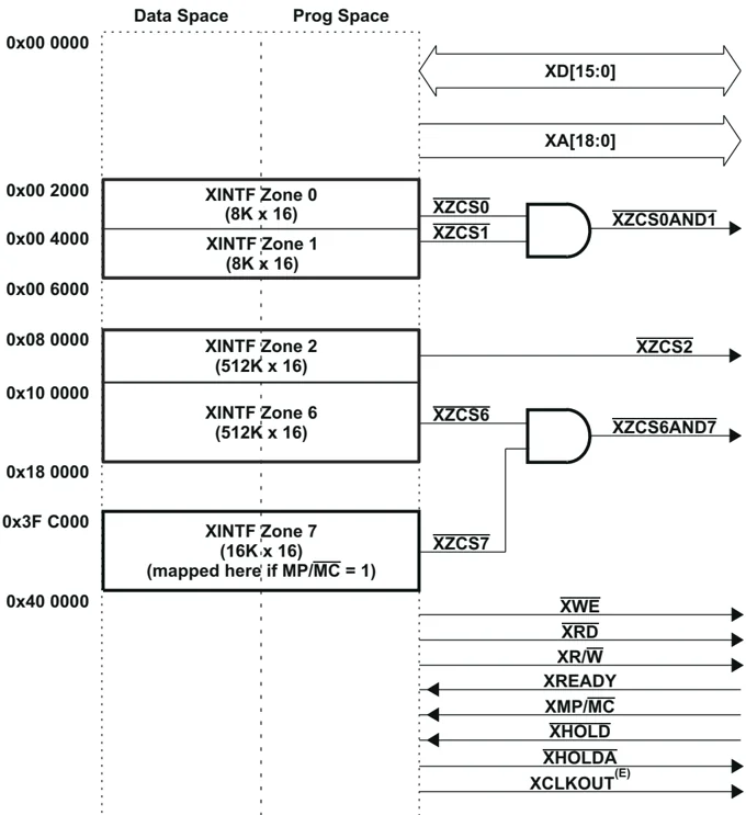
A. The mapping of XINTF Zone 7 is dependent on the XMP/ \overlineMC device input signal and the MP/ \overlineMC mode bit (bit 8 of XINTCNF2 register). Zones 0, 1, 2, and 6 are always enabled.
B. Each zone can be programmed with different wait states, setup and hold timing, and is supported by zone chip selects ( \overlineXZCS0AND1, \overlineXZCS2, \overlineXZCS6AND7), which toggle when an access to a particular zone is performed. These features enable glueless connection to many external memories and peripherals.
C. The chip selects for Zone 0 and Zone 1 are ANDed internally together to form one chip select ( \overlineXZCS0AND1). Any external memory that is connected to \overlineXZCS0AND1 is dually mapped to both Zone 0 and Zone 1.
D. The chip selects for Zone 6 and Zone 7 are ANDed internally together to form one chip select ( \overlineXZCS6AND7). Any external memory that is connected to \overlineXZCS6AND7 is dually mapped to both Zone 6 and Zone 7. This means that if Zone 7 is disabled (via the MP/ MC mode), then any external memory is still accessible via Zone 6 address space.
E. XCLKOUT is also pinned out on the F2810 and F2811 devices.
Figure 9-16. External Interface Block Diagram
Product Folder Links: TMS320F2810 TMS320F2810-Q1 TMS320F2811 TMS320F2811-Q1 TMS320F2812 TMS320F2812-Q1

The operation and timing of the external interface, can be controlled by the registers listed in Table 9-22.
Table 9-22. XINTF Configuration and Control Register Mappings
| NAME | ADDRESS | SIZE (x16) | DESCRIPTION |
|---|---|---|---|
| XTIMING0 | 0x00 0B20 | 2 | XINTF Timing Register, Zone 0 can access as two 16-bit registers or one 32-bit register. |
| XTIMING1 | 0x00 0B22 | 2 | XINTF Timing Register, Zone 1 can access as two 16-bit registers or one 32-bit register. |
| XTIMING2 | 0x00 0B24 | 2 | XINTF Timing Register, Zone 2 can access as two 16-bit registers or one 32-bit register. |
| XTIMING6 | 0x00 0B2C | 2 | XINTF Timing Register, Zone 6 can access as two 16-bit registers or one 32-bit register. |
| XTIMING7 | 0x00 0B2E | 2 | XINTF Timing Register, Zone 7 can access as two 16-bit registers or one 32-bit register. |
| XINTCNF2 | 0x00 0B34 | 2 | XINTF Configuration Register can access as two 16-bit registers or one 32-bit register. |
| XBANK | 0x00 0B38 | 1 | XINTF Bank Control Register |
| XREVISION | 0x00 0B3A | 1 | XINTF Revision Register |
9.6.1 Timing Registers
XINTF signal timing can be tuned to match specific external device requirements such as setup and hold times to strobe signals for contention avoidance and maximizing bus efficiency. The XINTF timing parameters can be configured individually for each zone based on the requirements of the memory or peripheral accessed by that particular zone. This allows the programmer to maximize the efficiency of the bus on a per-zone basis. All XINTF timing values are with respect to XTIMCLK, which is equal to or one-half of the SYSCLKOUT rate, as shown in Figure 8-26.
For detailed information on the XINTF timing and configuration register bit fields, see the TMS320x281x DSP External Interface (XINTF) Reference Guide.
9.6.2 XREVISION Register
The XREVISION register contains a unique number to identify the particular version of XINTF used in the product. For the F2812, this register will be configured as described in Table 9-23.
Table 9-23. XREVISION Register Bit Definitions
| BIT(S) | NAME | TYPE | RESET | DESCRIPTION |
|---|---|---|---|---|
| 15–0 | REVISION | R | 0x0004 | Current XINTF Revision. For internal use/reference. Test purposes only. Subject to change. |
9.7 Interrupts
Figure 9-17 shows how the various interrupt sources are multiplexed within the F281x devices.
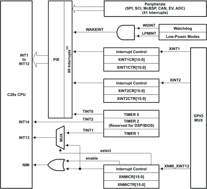
A. Out of a possible 96 interrupts, 45 are currently used by peripherals.
Figure 9-17. Interrupt Sources
Eight PIE block interrupts are grouped into one CPU interrupt. In total, 12 CPU interrupt groups, with 8 interrupts per group equals 96 possible interrupts. On the F281x, 45 of these are used by peripherals as shown in Table 9-24.
The TRAP #VectorNumber instruction transfers program control to the interrupt service routine corresponding to the vector specified. TRAP #0 attempts to transfer program control to the address pointed to by the reset vector. The PIE vector table does not, however, include a reset vector. Therefore, TRAP #0 should not be used when the PIE is enabled. Doing so will result in undefined behavior.
When the PIE is enabled, TRAP #1 through TRAP #12 will transfer program control to the interrupt service routine corresponding to the first vector within the PIE group. For example: TRAP #1 fetches the vector from INT1.1, TRAP #2 fetches the vector from INT2.1 and so forth.
TMS320F2810, TMS320F2810-Q1, TMS320F2811, TMS320F2811-Q1
TMS320F2812, TMS320F2812-Q1
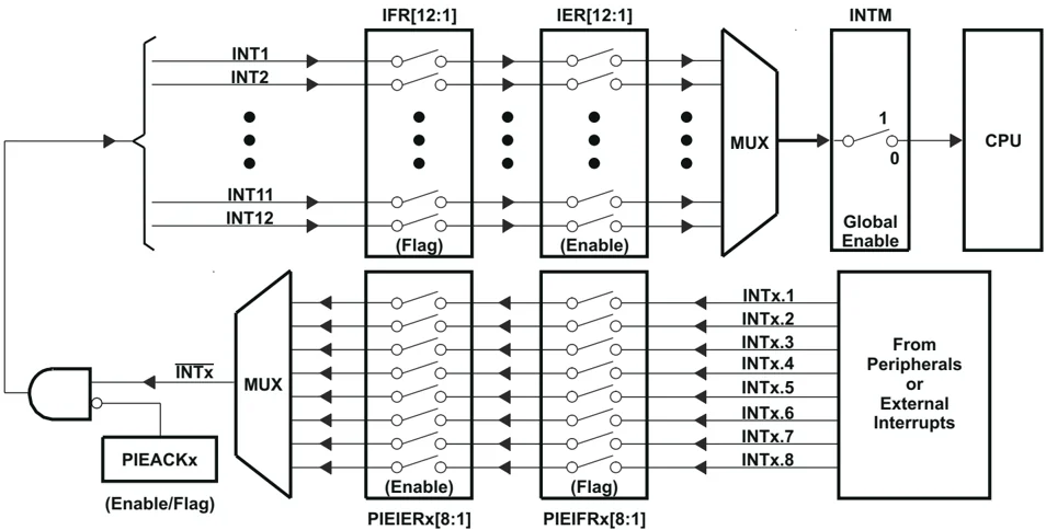
Figure 9-18. Multiplexing of Interrupts Using the PIE Block
Table 9-24. PIE Peripheral Interrupts
| CPU INTERRUPTS(1) | PIE INTERRUPTS | |||||||
|---|---|---|---|---|---|---|---|---|
| INTx.8 | INTx.7 | INTx.6 | INTx.5 | INTx.4 | INTx.3 | INTx.2 | INTx.1 | |
| INT1 | WAKEINT (LPM/WD) | TINT0 (TIMER 0) | ADCINT (ADC) | XINT2 | XINT1 | Reserved | PDPINTB (EV-B) | PDPINTA (EV-A) |
| INT2 | Reserved | T1OFINT (EV-A) | T1UFINT (EV-A) | T1CINT (EV-A) | T1PINT (EV-A) | CMP3INT (EV-A) | CMP2INT (EV-A) | CMP1INT (EV-A) |
| INT3 | Reserved | CAPINT3 (EV-A) | CAPINT2 (EV-A) | CAPINT1 (EV-A) | T2OFINT (EV-A) | T2UFINT (EV-A) | T2CINT (EV-A) | T2PINT (EV-A) |
| INT4 | Reserved | T3OFINT (EV-B) | T3UFINT (EV-B) | T3CINT (EV-B) | T3PINT (EV-B) | CMP6INT (EV-B) | CMP5INT (EV-B) | CMP4INT (EV-B) |
| INT5 | Reserved | CAPINT6 (EV-B) | CAPINT5 (EV-B) | CAPINT4 (EV-B) | T4OFINT (EV-B) | T4UFINT (EV-B) | T4CINT (EV-B) | T4PINT (EV-B) |
| INT6 | Reserved | Reserved | MXINT (McBSP) | MRINT (McBSP) | Reserved | Reserved | SPITXINTA (SPI) | SPIRXINTA (SPI) |
| INT7 | Reserved | Reserved | Reserved | Reserved | Reserved | Reserved | Reserved | Reserved |
| INT8 | Reserved | Reserved | Reserved | Reserved | Reserved | Reserved | Reserved | Reserved |
| INT9 | Reserved | Reserved | ECAN1INT (CAN) | ECAN0INT (CAN) | SCITXINTB (SCI-B) | SCIRXINTB (SCI-B) | SCITXINTA (SCI-A) | SCIRXINTA (SCI-A) |
| INT10 | Reserved | Reserved | Reserved | Reserved | Reserved | Reserved | Reserved | Reserved |
| INT11 | Reserved | Reserved | Reserved | Reserved | Reserved | Reserved | Reserved | Reserved |
| INT12 | Reserved | Reserved | Reserved | Reserved | Reserved | Reserved | Reserved | Reserved |
(1) Out of the 96 possible interrupts, 45 interrupts are currently used. The remaining interrupts are reserved for future devices. These interrupts can be used as software interrupts if they are enabled at the PIEIFRx level, provided none of the interrupts within the group is being used by a peripheral. Otherwise, interrupts coming in from peripherals may be lost by accidentally clearing their flag while modifying the PIEIFR.
To summarize, there are two safe cases when the reserved interrupts could be used as software interrupts:
a. No peripheral within the group is asserting interrupts.
b. No peripheral interrupts are assigned to the group (example PIE group 12).
Submit Document Feedback 137

Table 9-25. PIE Configuration and Control Registers
| NAME(1) | ADDRESS | SIZE (x16) | DESCRIPTION |
|---|---|---|---|
| PIECTRL | 0x0000 0CE0 | 1 | PIE, Control Register |
| PIEACK | 0x0000 0CE1 | 1 | PIE, Acknowledge Register |
| PIEIER1 | 0x0000 0CE2 | 1 | PIE, INT1 Group Enable Register |
| PIEIFR1 | 0x0000 0CE3 | 1 | PIE, INT1 Group Flag Register |
| PIEIER2 | 0x0000 0CE4 | 1 | PIE, INT2 Group Enable Register |
| PIEIFR2 | 0x0000 0CE5 | 1 | PIE, INT2 Group Flag Register |
| PIEIER3 | 0x0000 0CE6 | 1 | PIE, INT3 Group Enable Register |
| PIEIFR3 | 0x0000 0CE7 | 1 | PIE, INT3 Group Flag Register |
| PIEIER4 | 0x0000 0CE8 | 1 | PIE, INT4 Group Enable Register |
| PIEIFR4 | 0x0000 0CE9 | 1 | PIE, INT4 Group Flag Register |
| PIEIER5 | 0x0000 0CEA | 1 | PIE, INT5 Group Enable Register |
| PIEIFR5 | 0x0000 0CEB | 1 | PIE, INT5 Group Flag Register |
| PIEIER6 | 0x0000 0CEC | 1 | PIE, INT6 Group Enable Register |
| PIEIFR6 | 0x0000 0CED | 1 | PIE, INT6 Group Flag Register |
| PIEIER7 | 0x0000 0CEE | 1 | PIE, INT7 Group Enable Register |
| PIEIFR7 | 0x0000 0CEF | 1 | PIE, INT7 Group Flag Register |
| PIEIER8 | 0x0000 0CF0 | 1 | PIE, INT8 Group Enable Register |
| PIEIFR8 | 0x0000 0CF1 | 1 | PIE, INT8 Group Flag Register |
| PIEIER9 | 0x0000 0CF2 | 1 | PIE, INT9 Group Enable Register |
| PIEIFR9 | 0x0000 0CF3 | 1 | PIE, INT9 Group Flag Register |
| PIEIER10 | 0x0000 0CF4 | 1 | PIE, INT10 Group Enable Register |
| PIEIFR10 | 0x0000 0CF5 | 1 | PIE, INT10 Group Flag Register |
| PIEIER11 | 0x0000 0CF6 | 1 | PIE, INT11 Group Enable Register |
| PIEIFR11 | 0x0000 0CF7 | 1 | PIE, INT11 Group Flag Register |
| PIEIER12 | 0x0000 0CF8 | 1 | PIE, INT12 Group Enable Register |
| PIEIFR12 | 0x0000 0CF9 | 1 | PIE, INT12 Group Flag Register |
| Reserved | 0x0000 0CFA – 0x0000 0CFF | 6 | Reserved |
(1) The PIE configuration and control registers are not protected by EALLOW mode. The PIE vector table is protected.
9.7.1 External Interrupts
Table 9-26. External Interrupts Registers
| NAME | ADDRESS | SIZE (x16) | DESCRIPTION |
|---|---|---|---|
| XINT1CR | 0x00 7070 | 1 | XINT1 control register |
| XINT2CR | 0x00 7071 | 1 | XINT2 control register |
| Reserved | 0x00 7072 – 0x00 7076 | 5 | |
| XNMICR | 0x00 7077 | 1 | XNMI control register |
| XINT1CTR | 0x00 7078 | 1 | XINT1 counter register |
| XINT2CTR | 0x00 7079 | 1 | XINT2 counter register |
| Reserved | 0x00 707A – 0x00 707E | 5 | |
| XNMICTR | 0x00 707F | 1 | XNMI counter register |
Each external interrupt can be enabled/disabled or qualified using positive or negative going edge. For more information, see the TMS320x281x DSP System Control and Interrupts Reference Guide.
9.8 System Control
This section describes the F281x oscillator, PLL and clocking mechanisms, the watchdog function and the low-power modes. Figure 9-19 shows the various clock and reset domains in the F281x devices that will be discussed.
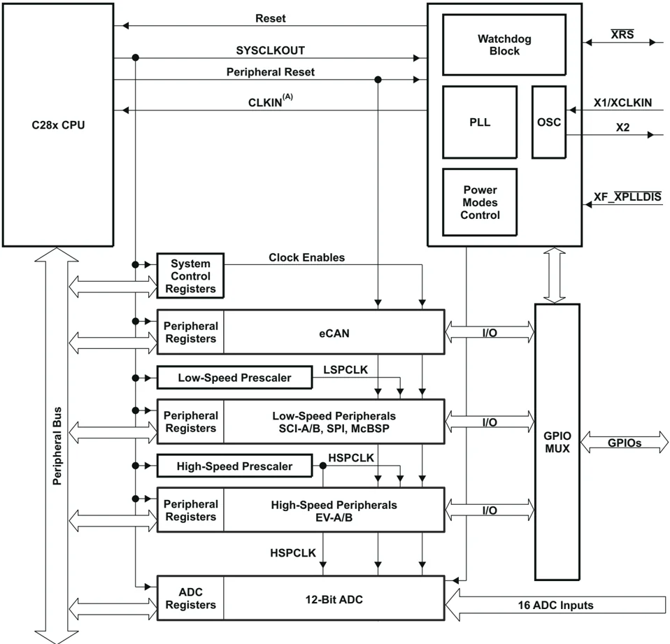
A. CLKIN is the clock input to the CPU. SYSCLKOUT is the output clock of the CPU. They are of the same frequency.
Figure 9-19. Clock and Reset Domains
TMS320F2810, TMS320F2810-Q1, TMS320F2811, TMS320F2811-Q1
TMS320F2812, TMS320F2812-Q1
The PLL, clocking, watchdog and low-power modes, are controlled by the registers listed in Table 9-27.
Table 9-27. PLL, Clocking, Watchdog, and Low-Power Mode Registers
| NAME(1) | ADDRESS | SIZE (x16) | DESCRIPTION |
|---|---|---|---|
| Reserved | 0x00 7010 – 0x00 7017 | 8 | |
| Reserved | 0x00 7018 | 1 | |
| Reserved | 0x00 7019 | 1 | |
| HISPCP | 0x00 701A | 1 | High-Speed Peripheral Clock Prescaler Register for HSPCLK clock |
| LOSPCP | 0x00 701B | 1 | Low-Speed Peripheral Clock Prescaler Register for LSPCLK clock |
| PCLKCR | 0x00 701C | 1 | Peripheral Clock Control Register |
| Reserved | 0x00 701D | 1 | |
| LPMCR0 | 0x00 701E | 1 | Low-Power Mode Control Register 0 |
| LPMCR1 | 0x00 701F | 1 | Low-Power Mode Control Register 1 |
| Reserved | 0x00 7020 | 1 | |
| PLLCR | 0x00 7021 | 1 | PLL Control Register(2) |
| SCSR | 0x00 7022 | 1 | System Control and Status Register |
| WDCNTR | 0x00 7023 | 1 | Watchdog Counter Register |
| Reserved | 0x00 7024 | 1 | |
| WDKEY | 0x00 7025 | 1 | Watchdog Reset Key Register |
| Reserved | 0x00 7026 – 0x00 7028 | 3 | |
| WDCR | 0x00 7029 | 1 | Watchdog Control Register |
| Reserved | 0x00 702A – 0x00 702F | 6 |
(1) All of the above registers can only be accessed by executing the EALLOW instruction.
(2) The PLL control register (PLLCR) is reset to a known state by the XRS signal only. Emulation reset (through Code Composer Studio) will not reset PLLCR.
Submit Document Feedback 141
9.9 OSC and PLL Block
Figure 9-20 shows the OSC and PLL block on F281x.
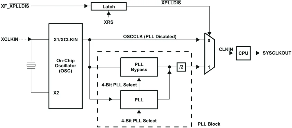
Figure 9-20. OSC and PLL Block
The on-chip oscillator circuit enables a crystal to be attached to the F281x devices using the X1/XCLKIN and X2 pins. If a crystal is not used, then an external oscillator can be directly connected to the X1/XCLKIN pin and the X2 pin is left unconnected. The logic-high level in this case should not exceed VDD. The PLLCR bits [3:0] set the clocking ratio.
TMS320F2810, TMS320F2810-Q1, TMS320F2811, TMS320F2811-Q1
Table 9-28. PLLCR Register Bit Definitions
(1) The PLLCR register is reset to a known state by the XRS reset line. If a reset is issued by the debugger, the PLL clocking ratio is not changed.
9.9.1 Loss of Input Clock
In PLL enabled mode, if the input clock XCLKIN or the oscillator clock is removed or absent, the PLL will still issue a "limp-mode" clock. The limp-mode clock will continue to clock the CPU and peripherals at a typical frequency of 1–4 MHz. The PLLCR register should have been written to with a non-zero value for this feature to work.
Normally, when the input clocks are present, the watchdog counter will decrement to initiate a watchdog reset or WDINT interrupt. However, when the external input clock fails, the watchdog counter will stop decrementing (that is, the watchdog counter does not change with the limp-mode clock). This condition could be used by the application firmware to detect the input clock failure and initiate necessary shut-down procedure for the system.
Note
Applications in which the correct CPU operating frequency is absolutely critical must implement a mechanism by which the DSP will be held in reset, should the input clocks ever fail. For example, an R-C circuit may be used to trigger the \overlineXRS pin of the DSP, should the capacitor ever get fully charged. An I/O pin may be used to discharge the capacitor on a periodic basis to prevent it from getting fully charged. Such a circuit would also help in detecting failure of the $V_{DD3VFL}$ rail.
TMS320F2810, TMS320F2810-Q1, TMS320F2811, TMS320F2811-Q1
9.10 PLL-Based Clock Module
The F281x has an on-chip, PLL-based clock module. This module provides all the necessary clocking signals for the device, as well as control for low-power mode entry. The PLL has a 4-bit ratio control to select different CPU clock rates. The watchdog module should be disabled before writing to the PLLCR register. It can be re-enabled (if need be) after the PLL module has stabilized, which takes 131072 XCLKIN cycles.
The PLL-based clock module provides two modes of operation:
- Crystal operation: This mode allows the use of an external crystal/resonator to provide the time base to the device.
- External clock source operation: This mode allows the internal oscillator to be bypassed. The device clocks are generated from an external clock source input on the X1/XCLKIN pin.
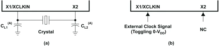
A. TI recommends that customers have the resonator/crystal vendor characterize the operation of their device with the DSP chip. The resonator/crystal vendor has the equipment and expertise to tune the tank circuit. The vendor can also advise the customer regarding the proper tank component values that will ensure start-up and stability over the entire operating range.
Figure 9-21. Recommended Crystal/Clock Connection
Table 9-29. Possible PLL Configuration Modes
9.11 External Reference Oscillator Clock Option
The typical specifications for the external quartz crystal for a frequency of 30 MHz are listed below:
- Fundamental mode, parallel resonant
- $C_L$ (load capacitance) = 12 pF
- $C_{L1} = C_{L2} = 24$ pF
- $C_{shunt} = 6$ pF
- ESR range = 25 to 40 \Omega
9.12 Watchdog Block
The watchdog block on the F281x is identical to the one used on the 240x devices. The watchdog module generates an output pulse, 512 oscillator clocks wide (OSCCLK), whenever the 8-bit watchdog up counter has reached its maximum value. To prevent this, the user disables the counter or the software must periodically write a 0x55 + 0xAA sequence into the watchdog key register which will reset the watchdog counter. Figure 9-22 shows the various functional blocks within the watchdog module.
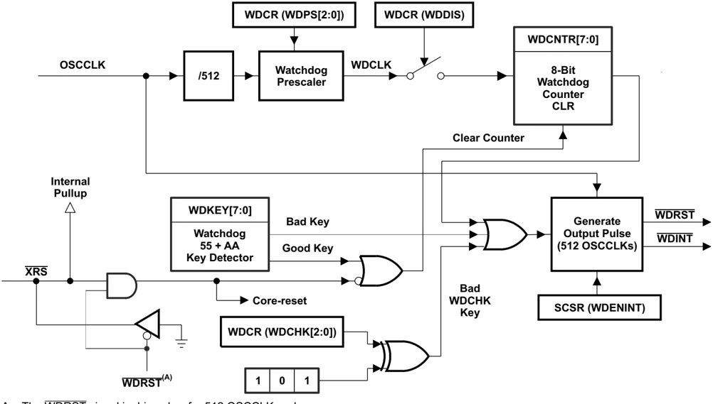
Figure 9-22. Watchdog Module
The \overlineWDINT signal enables the watchdog to be used as a wakeup from IDLE/STANDBY mode timer.
In STANDBY mode, all peripherals are turned off on the device. The only peripheral that remains functional is the watchdog. The WATCHDOG module will run off the PLL clock or the oscillator clock. The \overlineWDINT signal is fed to the LPM block so that it can wake the device from STANDBY (if enabled). See Section 9.13, Low-Power Modes Block, for more details.
In IDLE mode, the \overlineWDINT signal can generate an interrupt to the CPU, via the PIE, to take the CPU out of IDLE mode.
In HALT mode, this feature cannot be used because the oscillator (and PLL) are turned off and hence, so is the WATCHDOG.
9.13 Low-Power Modes Block
The low-power modes on F281x are similar to the 240x devices. Table 9-30 summarizes the various modes.
Table 9-30. Low-Power Modes
| MODE | LPM[1:0] | OSCCLK | CLKIN | SYSCLKOUT | EXIT⁽¹⁾ |
|---|---|---|---|---|---|
| Normal | X,X | on | on | on | – |
| IDLE | 0,0 | on | on | on⁽²⁾ | XRS, WDINT, Any Enabled Interrupt, XNMI, Debugger⁽³⁾ |
| STANDBY | 0,1 | on (watchdog still running) | off | off | XRS, WDINT, XINT1, XNMI, T1/2/3/4CTRIP, C1/2/3/4/5/6TRIP, SCIRXDA, SCIRXDB, CANRX, Debugger⁽³⁾ |
| HALT | 1,X | off (oscillator and PLL turned off, watchdog not functional) | off | off | XRS, XNMI, Debugger⁽³⁾ |
(1) The Exit column lists which signals or under what conditions the low-power mode will be exited. A low signal, on any of the signals, will exit the low-power condition. This signal must be kept low long enough for an interrupt to be recognized by the device. Otherwise, the IDLE mode will not be exited and the device will go back into the indicated low-power mode.
(2) The IDLE mode on the C28x behaves differently than on the 24x/240x. On the C28x, the clock output from the core (SYSCLKOUT) is still functional; while on the 24x/240x, the clock is turned off.
(3) On the C28x, the JTAG port can still function even if the core clock (CLKIN) is turned off.
The various low-power modes operate as follows:
IDLE Mode
This mode is exited by any enabled interrupt or an XNMI that is recognized by the processor. The LPM block performs no tasks during this mode as long as the LPMCR0(LPM) bits are set to 0,0.
STANDBY Mode
All other signals (including XNMI) will wake the device from STANDBY mode if selected by the LPMCR1 register. The user will need to select which signal(s) will wake the device. The selected signal(s) are also qualified by the OSCCLK before waking the device. The number of OSCCLKs is specified in the LPMCR0 register.
HALT Mode
Only the XRS and XNMI external signals can wake the device from HALT mode. The XNMI input to the core has an enable/disable bit. Hence, it is safe to use the XNMI signal for this function.
Note
The low-power modes do not affect the state of the output pins (PWM pins included). They will be in whatever state the code left them when the IDLE instruction was executed.