9.0 MASTER SYNCHRONOUS SERIAL PORT (MSSP) MODULE
9.1 Master SSP (MSSP) Module Overview
The Master Synchronous Serial Port (MSSP) module is a serial interface, useful for communicating with other peripheral or microcontroller devices. These peripheral devices may be serial EEPROMs, shift registers, display drivers, A/D converters, etc. The MSSP module can operate in one of two modes:
- Serial Peripheral Interface (SPI)
- Inter-Integrated Circuit (I$^2$C)
- Full Master mode
- Slave mode (with general address call)
The I$^2$C interface supports the following modes in hardware:
- Master mode
- Multi-Master mode
- Slave mode
9.2 Control Registers
The MSSP module has three associated registers. These include a status register (SSPSTAT) and two control registers (SSPCON and SSPCON2). The use of these registers and their individual configuration bits differ significantly, depending on whether the MSSP module is operated in SPI or I$^2$C mode.
Additional details are provided under the individual sections.
9.3 SPI Mode
The SPI mode allows 8 bits of data to be synchronously transmitted and received simultaneously. All four modes of SPI are supported. To accomplish communication, typically three pins are used:
- Serial Data Out (SDO) – RC5/SDO
- Serial Data In (SDI) – RC4/SDI/SDA
- Serial Clock (SCK) – RC3/SCK/SCL
Additionally, a fourth pin may be used when in a Slave mode of operation:
- Slave Select (\overlineSS) – RA5/AN4/\overlineSS/C2OUT
Figure 9-1 shows the block diagram of the MSSP module when operating in SPI mode.
FIGURE 9-1: MSSP BLOCK DIAGRAM (SPI MODE)
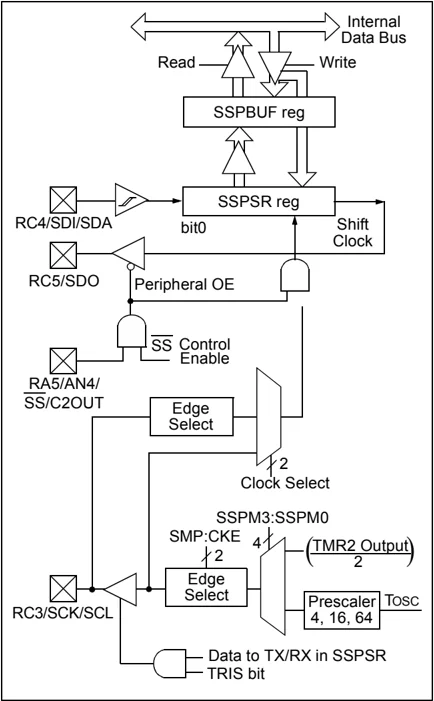
Note: When the SPI is in Slave mode with \overlineSS pin control enabled (SSPCON<3:0> = 0100), the state of the \overlineSS pin can affect the state read back from the TRISC<5> bit. The Peripheral OE signal from the SSP module in PORTC controls the state that is read back from the TRISC<5> bit (see Section 4.3 “PORTC and the TRISC Register” for information on PORTC). If Read-Modify-Write instructions, such as BSF, are performed on the TRISC register while the \overlineSS pin is high, this will cause the TRISC<5> bit to be set, thus disabling the SDO output.
9.3.1 REGISTERS
The MSSP module has four registers for SPI mode operation. These are:
- MSSP Control Register (SSPCON)
- MSSP Status Register (SSPSTAT)
- Serial Receive/Transmit Buffer Register (SSPBUF)
- MSSP Shift Register (SSPSR) – Not directly accessible
SSPCON and SSPSTAT are the control and status registers in SPI mode operation. The SSPCON register is readable and writable. The lower six bits of the SSPSTAT are read-only. The upper two bits of the SSPSTAT are read/write.
SSPSR is the shift register used for shifting data in or out. SSPBUF is the buffer register to which data bytes are written to or read from.
In receive operations, SSPSR and SSPBUF together create a double-buffered receiver. When SSPSR receives a complete byte, it is transferred to SSPBUF and the SSPIF interrupt is set.
During transmission, the SSPBUF is not double-buffered. A write to SSPBUF will write to both SSPBUF and SSPSR.
REGISTER 9-1: SSPSTAT: MSSP STATUS REGISTER (SPI MODE) (ADDRESS 94h)
| R/W-0 | R/W-0 | R-0 | R-0 | R-0 | R-0 | R-0 | R-0 |
|---|---|---|---|---|---|---|---|
| SMP | CKE | D/A | P | S | R/W | UA | BF |
| bit 7 | bit 0 |
bit 7
SMP: Sample bit
SPI Master mode:
1 = Input data sampled at end of data output time
0 = Input data sampled at middle of data output time
SPI Slave mode:
SMP must be cleared when SPI is used in Slave mode.
bit 6
CKE: SPI Clock Select bit
1 = Transmit occurs on transition from active to Idle clock state
0 = Transmit occurs on transition from Idle to active clock state
Note: Polarity of clock state is set by the CKP bit (SSPCON1<4>).
bit 5
D/A: Data/Address bit
Used in I²C mode only.
bit 4
P: Stop bit
Used in I²C mode only. This bit is cleared when the MSSP module is disabled, SSPEN is cleared.
bit 3
S: Start bit
Used in I²C mode only.
bit 2
R/W: Read/Write bit information
Used in I²C mode only.
bit 1
UA: Update Address bit
Used in I²C mode only.
bit 0
BF: Buffer Full Status bit (Receive mode only)
1 = Receive complete, SSPBUF is full
0 = Receive not complete, SSPBUF is empty
Legend:
R = Readable bit
W = Writable bit
U = Unimplemented bit, read as ‘0’
- n = Value at POR
‘1’ = Bit is set
‘0’ = Bit is cleared
x = Bit is unknown
REGISTER 9-2: SSPCON1: MSSP CONTROL REGISTER 1 (SPI MODE) (ADDRESS 14h)
| R/W-0 | R/W-0 | R/W-0 | R/W-0 | R/W-0 | R/W-0 | R/W-0 | R/W-0 |
|---|---|---|---|---|---|---|---|
| WCOL | SSPOV | SSPEN | CKP | SSPM3 | SSPM2 | SSPM1 | SSPM0 |
| bit 7 | bit 0 |
bit 7
WCOL: Write Collision Detect bit (Transmit mode only)
- 1 = The SSPBUF register is written while it is still transmitting the previous word. (Must be cleared in software.)
- 0 = No collision
bit 6
SSPOV: Receive Overflow Indicator bit
SPI Slave mode:
- 1 = A new byte is received while the SSPBUF register is still holding the previous data. In case of overflow, the data in SSPSR is lost. Overflow can only occur in Slave mode. The user must read the SSPBUF, even if only transmitting data, to avoid setting overflow. (Must be cleared in software.)
- 0 = No overflow
Note: In Master mode, the overflow bit is not set, since each new reception (and transmission) is initiated by writing to the SSPBUF register.
bit 5
SSPEN: Synchronous Serial Port Enable bit
- 1 = Enables serial port and configures SCK, SDO, SDI, and \overlineSS as serial port pins
- 0 = Disables serial port and configures these pins as I/O port pins
Note: When enabled, these pins must be properly configured as input or output.
bit 4
CKP: Clock Polarity Select bit
- 1 = Idle state for clock is a high level
- 0 = Idle state for clock is a low level
bit 3-0
SSPM3:SSPM0: Synchronous Serial Port Mode Select bits
- 0101 = SPI Slave mode, clock = SCK pin. \overlineSS pin control disabled. \overlineSS can be used as I/O pin.
- 0100 = SPI Slave mode, clock = SCK pin. \overlineSS pin control enabled.
- 0011 = SPI Master mode, clock = TMR2 output/2
- 0010 = SPI Master mode, clock = Fosc/64
- 0001 = SPI Master mode, clock = Fosc/16
- 0000 = SPI Master mode, clock = Fosc/4
Note: Bit combinations not specifically listed here are either reserved or implemented in I²C mode only.
Legend:
| R = Readable bit | W = Writable bit | U = Unimplemented bit, read as ‘0’ |
|---|---|---|
| - n = Value at POR | ‘1’ = Bit is set | ‘0’ = Bit is cleared x = Bit is unknown |
9.3.2 OPERATION
When initializing the SPI, several options need to be specified. This is done by programming the appropriate control bits (SSPCON<5:0> and SSPSTAT<7:6>). These control bits allow the following to be specified:
- Master mode (SCK is the clock output)
- Slave mode (SCK is the clock input)
- Clock Polarity (Idle state of SCK)
- Data Input Sample Phase (middle or end of data output time)
- Clock Edge (output data on rising/falling edge of SCK)
- Clock Rate (Master mode only)
- Slave Select mode (Slave mode only)
The MSSP consists of a transmit/receive shift register (SSPSR) and a buffer register (SSPBUF). The SSPSR shifts the data in and out of the device, MSb first. The SSPBUF holds the data that was written to the SSPSR until the received data is ready. Once the eight bits of data have been received, that byte is moved to the SSPBUF register. Then, the Buffer Full detect bit, BF (SSPSTAT<0>), and the interrupt flag bit, SSPIF, are set. This double-buffering of the received data (SSPBUF) allows the next byte to start reception before reading the data that was just received. Any write to the SSPBUF register during transmission/reception of data will be ignored and the write collision detect bit, WCOL (SSPCON<7>), will be set. User software must clear the WCOL bit so that it can be determined if the following write(s) to the SSPBUF register completed successfully.
When the application software is expecting to receive valid data, the SSPBUF should be read before the next byte of data to transfer is written to the SSPBUF. Buffer Full bit, BF (SSPSTAT<0>), indicates when SSPBUF has been loaded with the received data (transmission is complete). When the SSPBUF is read, the BF bit is cleared. This data may be irrelevant if the SPI is only a transmitter. Generally, the MSSP interrupt is used to determine when the transmission/reception has completed. The SSPBUF must be read and/or written. If the interrupt method is not going to be used, then software polling can be done to ensure that a write collision does not occur. Example 9-1 shows the loading of the SSPBUF (SSPSR) for data transmission.
The SSPSR is not directly readable or writable and can only be accessed by addressing the SSPBUF register. Additionally, the MSSP Status register (SSPSTAT) indicates the various status conditions.
EXAMPLE 9-1: LOADING THE SSPBUF (SSPSR) REGISTER
DS39582C-page 74 © 2001-2013 Microchip Technology Inc.
9.3.3 ENABLING SPI I/O
To enable the serial port, SSP Enable bit, SSPEN (SSPCON<5>), must be set. To reset or reconfigure SPI mode, clear the SSPEN bit, re-initialize the SSPCON registers and then set the SSPEN bit. This configures the SDI, SDO, SCK and \overlineSS pins as serial port pins. For the pins to behave as the serial port function, some must have their data direction bits (in the TRIS register) appropriately programmed. That is:
- SDI is automatically controlled by the SPI module
- SDO must have TRISC<5> bit cleared
- SCK (Master mode) must have TRISC<3> bit cleared
- SCK (Slave mode) must have TRISC<3> bit set
- \overlineSS must have TRISC<4> bit set
Any serial port function that is not desired may be overridden by programming the corresponding data direction (TRIS) register to the opposite value.
9.3.4 TYPICAL CONNECTION
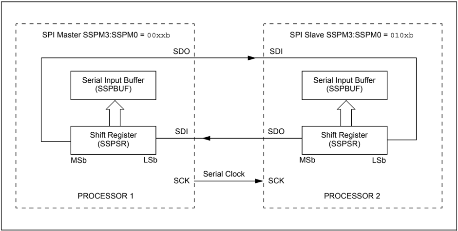
Figure 9-2 shows a typical connection between two microcontrollers. The master controller (Processor 1) initiates the data transfer by sending the SCK signal. Data is shifted out of both shift registers on their programmed clock edge and latched on the opposite edge of the clock. Both processors should be programmed to the same Clock Polarity (CKP), then both controllers would send and receive data at the same time. Whether the data is meaningful (or dummy data) depends on the application software. This leads to three scenarios for data transmission:
- Master sends data – Slave sends dummy data
- Master sends data – Slave sends data
- Master sends dummy data – Slave sends data
FIGURE 9-2: SPI MASTER/SLAVE CONNECTION
9.3.5 MASTER MODE
The master can initiate the data transfer at any time because it controls the SCK. The master determines when the slave (Processor 2, Figure 9-2) is to broadcast data by the software protocol.
In Master mode, the data is transmitted/received as soon as the SSPBUF register is written to. If the SPI is only going to receive, the SDO output could be disabled (programmed as an input). The SSPSR register will continue to shift in the signal present on the SDI pin at the programmed clock rate. As each byte is received, it will be loaded into the SSPBUF register as if a normal received byte (interrupts and status bits appropriately set). This could be useful in receiver applications as a "Line Activity Monitor" mode.
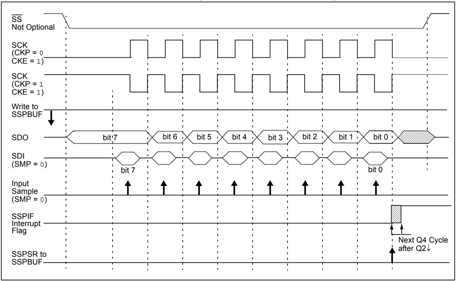
The clock polarity is selected by appropriately programming the CKP bit (SSPCON<4>). This then, would give waveforms for SPI communication as shown in Figure 9-3, Figure 9-5 and Figure 9-6, where the MSB is transmitted first. In Master mode, the SPI clock rate (bit rate) is user programmable to be one of the following:
- Fosc/4 (or Tcy)
- Fosc/16 (or 4 • Tcy)
- Fosc/64 (or 16 • Tcy)
- Timer2 output/2
This allows a maximum data rate (at 40 MHz) of 10.00 Mbps.
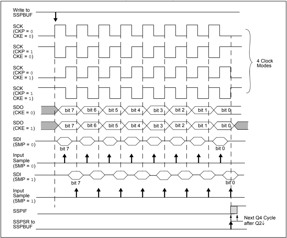
Figure 9-3 shows the waveforms for Master mode. When the CKE bit is set, the SDO data is valid before there is a clock edge on SCK. The change of the input sample is shown based on the state of the SMP bit. The time when the SSPBUF is loaded with the received data is shown.
FIGURE 9-3: SPI MODE WAVEFORM (MASTER MODE)
DS39582C-page 76 © 2001-2013 Microchip Technology Inc.
9.3.6 SLAVE MODE
In Slave mode, the data is transmitted and received as the external clock pulses appear on SCK. When the last bit is latched, the SSPIF interrupt flag bit is set.
While in Slave mode, the external clock is supplied by the external clock source on the SCK pin. This external clock must meet the minimum high and low times as specified in the electrical specifications.
While in Sleep mode, the slave can transmit/receive data. When a byte is received, the device will wake-up from Sleep.
9.3.7 SLAVE SELECT SYNCHRONIZATION
The \overlineSS pin allows a Synchronous Slave mode. The SPI must be in Slave mode with \overlineSS pin control enabled (SSPCON<3:0> = 04h). The pin must not be driven low for the \overlineSS pin to function as an input. The data latch must be high. When the \overlineSS pin is low, transmission and reception are enabled and the SDO pin is driven. When the \overlineSS pin goes high, the SDO pin is no longer driven even if in the middle of a transmitted byte and becomes a floating output. External pull-up/pull-down resistors may be desirable, depending on the application.
Note 1: When the SPI is in Slave mode with \overlineSS pin control enabled (SSPCON<3:0> = 0100), the SPI module will reset if the \overlineSS pin is set to VDD.
2: If the SPI is used in Slave Mode with CKE set, then the \overlineSS pin control must be enabled.
When the SPI module resets, the bit counter is forced to '0'. This can be done by either forcing the SS pin to a high level or clearing the SSPEN bit.
To emulate two-wire communication, the SDO pin can be connected to the SDI pin. When the SPI needs to operate as a receiver, the SDO pin can be configured as an input. This disables transmissions from the SDO. The SDI can always be left as an input (SDI function) since it cannot create a bus conflict.
FIGURE 9-4: SLAVE SYNCHRONIZATION WAVEFORM
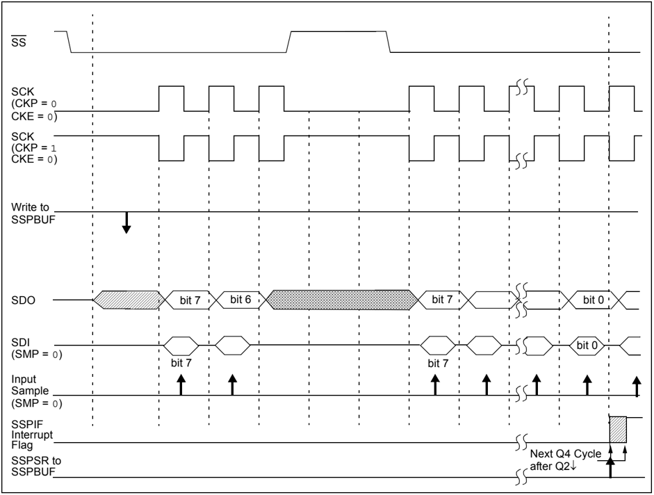
FIGURE 9-5: SPI MODE WAVEFORM (SLAVE MODE WITH CKE = 0)
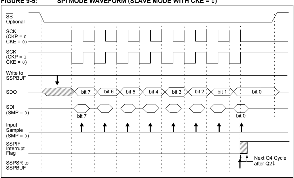
FIGURE 9-6: SPI MODE WAVEFORM (SLAVE MODE WITH CKE = 1)
DS39582C-page 78 © 2001-2013 Microchip Technology Inc.
9.3.8 SLEEP OPERATION
In Master mode, all module clocks are halted and the transmission/reception will remain in that state until the device wakes from Sleep. After the device returns to normal mode, the module will continue to transmit/receive data.
In Slave mode, the SPI Transmit/Receive Shift register operates asynchronously to the device. This allows the device to be placed in Sleep mode and data to be shifted into the SPI Transmit/Receive Shift register. When all 8 bits have been received, the MSSP interrupt flag bit will be set and if enabled, will wake the device from Sleep.
9.3.9 EFFECTS OF A RESET
A Reset disables the MSSP module and terminates the current transfer.
9.3.10 BUS MODE COMPATIBILITY
Table 9-1 shows the compatibility between the standard SPI modes and the states of the CKP and CKE control bits.
TABLE 9-1: SPI BUS MODES
| Standard SPI Mode Terminology | Control Bits State | |
|---|---|---|
| CKP | CKE | |
| 0, 0 | 0 | 1 |
| 0, 1 | 0 | 0 |
| 1, 0 | 1 | 1 |
| 1, 1 | 1 | 0 |
There is also a SMP bit which controls when the data is sampled.
TABLE 9-2: REGISTERS ASSOCIATED WITH SPI OPERATION
| Name | Bit 7 | Bit 6 | Bit 5 | Bit 4 | Bit 3 | Bit 2 | Bit 1 | Bit 0 | Value on POR, BOR | Value on all other Resets |
|---|---|---|---|---|---|---|---|---|---|---|
| INTCON | GIE/GIEH | PEIE/GIEL | TMR0IE | INT0IE | RBIE | TMR0IF | INT0IF | RBIF | 0000 000x | 0000 000u |
| PIR1 | PSPIF(1) | ADIF | RCIF | TXIF | SSPIF | CCP1IF | TMR2IF | TMR1IF | 0000 0000 | 0000 0000 |
| PIE1 | PSPIE(1) | ADIE | RCIE | TXIE | SSPIE | CCP1IE | TMR2IE | TMR1IE | 0000 0000 | 0000 0000 |
| TRISC | PORTC Data Direction Register | 1111 1111 | 1111 1111 | |||||||
| SSPBUF | Synchronous Serial Port Receive Buffer/Transmit Register | xxxx xxxx | uuuu uuuu | |||||||
| SSPCON | WCOL | SSPOV | SSPEN | CKP | SSPM3 | SSPM2 | SSPM1 | SSPM0 | 0000 0000 | 0000 0000 |
| TRISA | — | PORTA Data Direction Register | --11 1111 | --11 1111 | ||||||
| SSPSTAT | SMP | CKE | D/Ā | P | S | R/Ŵ | UA | BF | 0000 0000 | 0000 0000 |
Legend: x = unknown, u = unchanged, - = unimplemented, read as ‘0’.
Shaded cells are not used by the MSSP in SPI mode.
Note 1: The PSPIF, PSPIE and PSPIP bits are reserved on 28-pin devices; always maintain these bits clear.
9.4 I²C Mode
The MSSP module in I²C mode fully implements all master and slave functions (including general call support) and provides interrupts on Start and Stop bits in hardware to determine a free bus (multi-master function). The MSSP module implements the standard mode specifications, as well as 7-bit and 10-bit addressing.
Two pins are used for data transfer:
- Serial clock (SCL) – RC3/SCK/SCL
- Serial data (SDA) – RC4/SDI/SDA
The user must configure these pins as inputs or outputs through the TRISC<4:3> bits.
FIGURE 9-7: MSSP BLOCK DIAGRAM (I²C MODE)
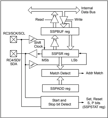
9.4.1 REGISTERS
The MSSP module has six registers for I²C operation. These are:
- MSSP Control Register (SSPCON)
- MSSP Control Register 2 (SSPCON2)
- MSSP Status Register (SSPSTAT)
- Serial Receive/Transmit Buffer Register (SSPBUF)
- MSSP Shift Register (SSPSR) – Not directly accessible
- MSSP Address Register (SSPADD)
SSPCON, SSPCON2 and SSPSTAT are the control and status registers in I²C mode operation. The SSPCON and SSPCON2 registers are readable and writable. The lower six bits of the SSPSTAT are read-only. The upper two bits of the SSPSTAT are read/write.
SSPSR is the shift register used for shifting data in or out. SSPBUF is the buffer register to which data bytes are written to or read from.
SSPADD register holds the slave device address when the SSP is configured in I²C Slave mode. When the SSP is configured in Master mode, the lower seven bits of SSPADD act as the baud rate generator reload value.
In receive operations, SSPSR and SSPBUF together create a double-buffered receiver. When SSPSR receives a complete byte, it is transferred to SSPBUF and the SSPIF interrupt is set.
During transmission, the SSPBUF is not double-buffered. A write to SSPBUF will write to both SSPBUF and SSPSR.
REGISTER 9-3: SSPSTAT: MSSP STATUS REGISTER (I²C MODE) (ADDRESS 94h)
| R/W-0 | R/W-0 | R-0 | R-0 | R-0 | R-0 | R-0 | R-0 |
|---|---|---|---|---|---|---|---|
| SMP | CKE | D/Ā | P | S | R/Ŵ | UA | BF |
| bit 7 | bit 0 |
bit 7
SMP: Slew Rate Control bit
In Master or Slave mode:
- 1 = Slew rate control disabled for standard speed mode (100 kHz and 1 MHz)
- 0 = Slew rate control enabled for high-speed mode (400 kHz)
bit 6
CKE: SMBus Select bit
In Master or Slave mode:
- 1 = Enable SMBus specific inputs
- 0 = Disable SMBus specific inputs
bit 5
D/Ā: Data/Address bit
In Master mode:
- Reserved.
In Slave mode:
- 1 = Indicates that the last byte received or transmitted was data
- 0 = Indicates that the last byte received or transmitted was address
bit 4
P: Stop bit
- 1 = Indicates that a Stop bit has been detected last
- 0 = Stop bit was not detected last
Note: This bit is cleared on Reset and when SSPEN is cleared.
bit 3
S: Start bit
- 1 = Indicates that a Start bit has been detected last
- 0 = Start bit was not detected last
Note: This bit is cleared on Reset and when SSPEN is cleared.
bit 2
R/Ŵ: Read/Write bit information (I²C mode only)
In Slave mode:
- 1 = Read
- 0 = Write
Note: This bit holds the R/Ŵ bit information following the last address match. This bit is only valid from the address match to the next Start bit, Stop bit or not ACK bit.
In Master mode:
- 1 = Transmit is in progress
- 0 = Transmit is not in progress
Note: ORing this bit with SEN, RSEN, PEN, RCEN or ACKEN will indicate if the MSSP is in Idle mode.
bit 1
UA: Update Address (10-bit Slave mode only)
- 1 = Indicates that the user needs to update the address in the SSPADD register
- 0 = Address does not need to be updated
bit 0
BF: Buffer Full Status bit
In Transmit mode:
- 1 = Receive complete, SSPBUF is full
- 0 = Receive not complete, SSPBUF is empty
In Receive mode:
- 1 = Data Transmit in progress (does not include the ACK and Stop bits), SSPBUF is full
- 0 = Data Transmit complete (does not include the ACK and Stop bits), SSPBUF is empty
Legend:
- R = Readable bit
- W = Writable bit
- U = Unimplemented bit, read as ‘0’
-
- n = Value at POR
- ‘1’ = Bit is set
- ‘0’ = Bit is cleared
- x = Bit is unknown
REGISTER 9-4: SSPCON1: MSSP CONTROL REGISTER 1 (I²C MODE) (ADDRESS 14h)
| R/W-0 | R/W-0 | R/W-0 | R/W-0 | R/W-0 | R/W-0 | R/W-0 | R/W-0 |
|---|---|---|---|---|---|---|---|
| WCOL | SSPOV | SSPEN | CKP | SSPM3 | SSPM2 | SSPM1 | SSPM0 |
| bit 7 | bit 0 |
bit 7
WCOL: Write Collision Detect bit
In Master Transmit mode:
- 1 = A write to the SSPBUF register was attempted while the I²C conditions were not valid for a transmission to be started. (Must be cleared in software.)
- 0 = No collision
In Slave Transmit mode:
- 1 = The SSPBUF register is written while it is still transmitting the previous word. (Must be cleared in software.)
- 0 = No collision
In Receive mode (Master or Slave modes):
- This is a “don’t care” bit.
bit 6
SSPOV: Receive Overflow Indicator bit
In Receive mode:
- 1 = A byte is received while the SSPBUF register is still holding the previous byte. (Must be cleared in software.)
- 0 = No overflow
In Transmit mode:
- This is a “don’t care” bit in Transmit mode.
bit 5
SSPEN: Synchronous Serial Port Enable bit
- 1 = Enables the serial port and configures the SDA and SCL pins as the serial port pins
- 0 = Disables the serial port and configures these pins as I/O port pins
Note: When enabled, the SDA and SCL pins must be properly configured as input or output.
bit 4
CKP: SCK Release Control bit
In Slave mode:
- 1 = Release clock
- 0 = Holds clock low (clock stretch). (Used to ensure data setup time.)
In Master mode:
- Unused in this mode.
bit 3-0
SSPM3:SSPM0: Synchronous Serial Port Mode Select bits
- 1111 = I²C Slave mode, 10-bit address with Start and Stop bit interrupts enabled
- 1110 = I²C Slave mode, 7-bit address with Start and Stop bit interrupts enabled
- 1011 = I²C Firmware Controlled Master mode (Slave Idle)
- 1000 = I²C Master mode, clock = FOSC/(4 * (SSPADD + 1))
- 0111 = I²C Slave mode, 10-bit address
- 0110 = I²C Slave mode, 7-bit address
Note: Bit combinations not specifically listed here are either reserved or implemented in SPI mode only.
Legend:
| R = Readable bit | W = Writable bit | U = Unimplemented bit, read as ‘0’ |
|---|---|---|
| - n = Value at POR | ‘1’ = Bit is set | ‘0’ = Bit is cleared x = Bit is unknown |
REGISTER 9-5: SSPCON2: MSSP CONTROL REGISTER 2 (I²C MODE) (ADDRESS 91h)
| R/W-0 | R/W-0 | R/W-0 | R/W-0 | R/W-0 | R/W-0 | R/W-0 | R/W-0 |
|---|---|---|---|---|---|---|---|
| GCEN | ACKSTAT | ACKDT | ACKEN | RCEN | PEN | RSEN | SEN |
| bit 7 | bit 0 |
bit 7
GCEN: General Call Enable bit (Slave mode only)
1 = Enable interrupt when a general call address (0000h) is received in the SSPSR
0 = General call address disabled
bit 6
ACKSTAT: Acknowledge Status bit (Master Transmit mode only)
1 = Acknowledge was not received from slave
0 = Acknowledge was received from slave
bit 5
ACKDT: Acknowledge Data bit (Master Receive mode only)
1 = Not Acknowledge
0 = Acknowledge
Note: Value that will be transmitted when the user initiates an Acknowledge sequence at the end of a receive.
bit 4
ACKEN: Acknowledge Sequence Enable bit (Master Receive mode only)
1 = Initiate Acknowledge sequence on SDA and SCL pins and transmit ACKDT data bit. Automatically cleared by hardware.
0 = Acknowledge sequence Idle
bit 3
RCEN: Receive Enable bit (Master mode only)
1 = Enables Receive mode for I²C
0 = Receive Idle
bit 2
PEN: Stop Condition Enable bit (Master mode only)
1 = Initiate Stop condition on SDA and SCL pins. Automatically cleared by hardware.
0 = Stop condition Idle
bit 1
RSEN: Repeated Start Condition Enabled bit (Master mode only)
1 = Initiate Repeated Start condition on SDA and SCL pins. Automatically cleared by hardware.
0 = Repeated Start condition Idle
bit 0
SEN: Start Condition Enabled/Stretch Enabled bit
In Master mode:
1 = Initiate Start condition on SDA and SCL pins. Automatically cleared by hardware.
0 = Start condition Idle
In Slave mode:
1 = Clock stretching is enabled for both slave transmit and slave receive (stretch enabled)
0 = Clock stretching is enabled for slave transmit only (PIC16F87X compatibility)
Legend:
R = Readable bit
W = Writable bit
U = Unimplemented bit, read as ‘0’
- n = Value at POR
‘1’ = Bit is set
‘0’ = Bit is cleared
x = Bit is unknown
Note: For bits ACKEN, RCEN, PEN, RSEN, SEN: If the I²C module is not in the Idle mode, this bit may not be set (no spooling) and the SSPBUF may not be written (or writes to the SSPBUF are disabled).
9.4.2 OPERATION
The MSSP module functions are enabled by setting MSSP Enable bit, SSPEN (SSPCON<5>).
The SSPCON register allows control of the I$^2$C operation. Four mode selection bits (SSPCON<3:0>) allow one of the following I$^2$C modes to be selected:
- I$^2$C Master mode, clock = OSC/4 (SSPADD + 1)
- I$^2$C Slave mode (7-bit address)
- I$^2$C Slave mode (10-bit address)
- I$^2$C Slave mode (7-bit address) with Start and Stop bit interrupts enabled
- I$^2$C Slave mode (10-bit address) with Start and Stop bit interrupts enabled
- I$^2$C Firmware Controlled Master mode, slave is Idle
Selection of any I$^2$C mode, with the SSPEN bit set, forces the SCL and SDA pins to be open-drain, provided these pins are programmed to inputs by setting the appropriate TRISC bits. To ensure proper operation of the module, pull-up resistors must be provided externally to the SCL and SDA pins.
9.4.3 SLAVE MODE
In Slave mode, the SCL and SDA pins must be configured as inputs (TRISC<4:3> set). The MSSP module will override the input state with the output data when required (slave-transmitter).
The I$^2$C Slave mode hardware will always generate an interrupt on an address match. Through the mode select bits, the user can also choose to interrupt on Start and Stop bits
When an address is matched, or the data transfer after an address match is received, the hardware automatically will generate the Acknowledge (\overlineACK) pulse and load the SSPBUF register with the received value currently in the SSPSR register.
Any combination of the following conditions will cause the MSSP module not to give this \overlineACK pulse:
- The buffer full bit, BF (SSPSTAT<0>), was set before the transfer was received.
- The overflow bit, SSPOV (SSPCON<6>), was set before the transfer was received.
In this case, the SSPSR register value is not loaded into the SSPBUF, but bit SSPIF (PIR1<3>) is set. The BF bit is cleared by reading the SSPBUF register, while bit SSPOV is cleared through software.
The SCL clock input must have a minimum high and low for proper operation. The high and low times of the I$^2$C specification, as well as the requirement of the MSSP module, are shown in timing parameter #100 and parameter #101.
9.4.3.1 Addressing
Once the MSSP module has been enabled, it waits for a Start condition to occur. Following the Start condition, the 8 bits are shifted into the SSPSR register. All incoming bits are sampled with the rising edge of the clock (SCL) line. The value of register SSPSR<7:1> is compared to the value of the SSPADD register. The address is compared on the falling edge of the eighth clock (SCL) pulse. If the addresses match, and the BF and SSPOV bits are clear, the following events occur:
- The SSPSR register value is loaded into the SSPBUF register.
- The Buffer Full bit, BF, is set.
- An \overlineACK pulse is generated.
- MSSP Interrupt Flag bit, SSPIF (PIR1<3>), is set (interrupt is generated if enabled) on the falling edge of the ninth SCL pulse.
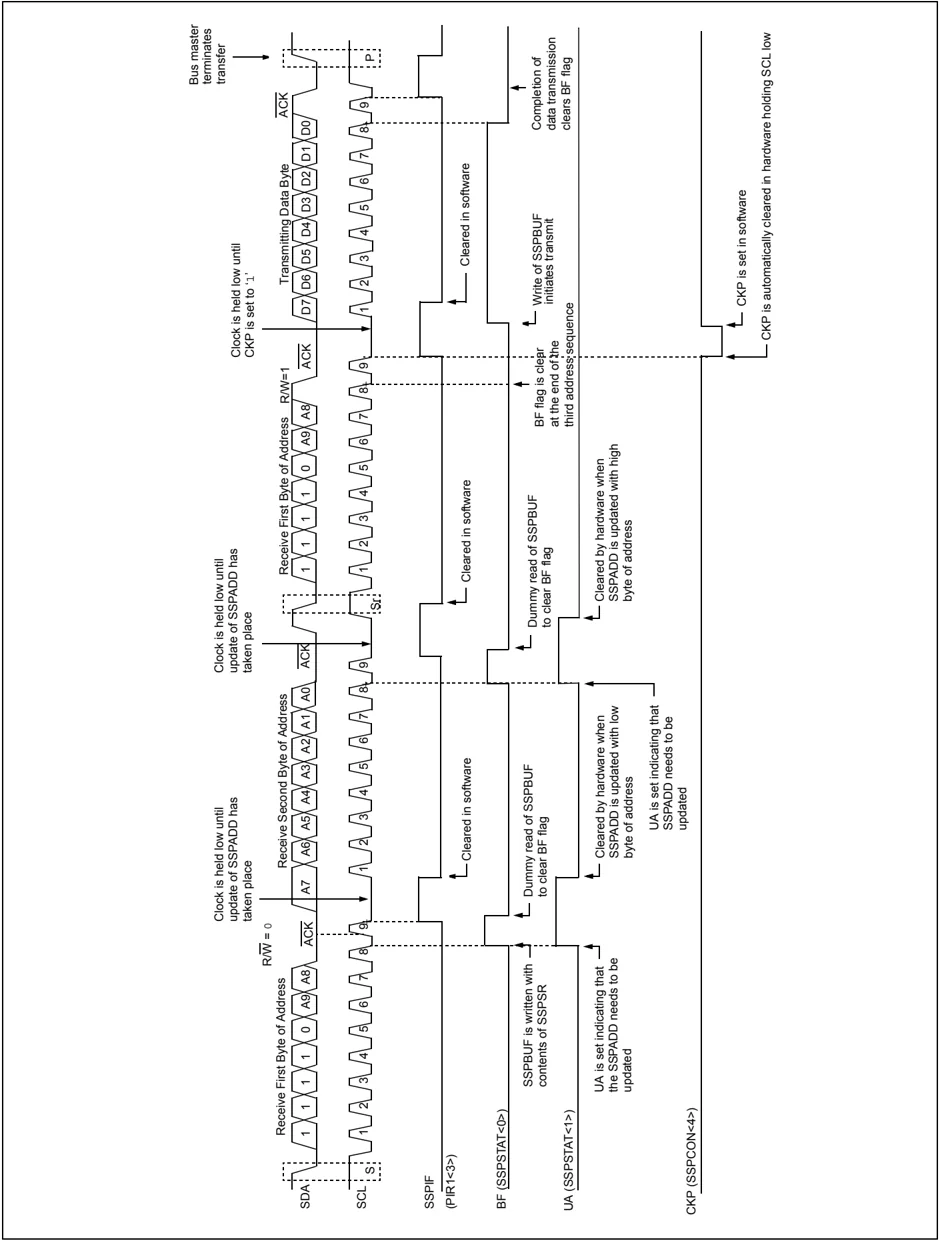
In 10-bit Address mode, two address bytes need to be received by the slave. The five Most Significant bits (MSbs) of the first address byte specify if this is a 10-bit address. Bit R/\overlineW (SSPSTAT<2>) must specify a write so the slave device will receive the second address byte. For a 10-bit address, the first byte would equal '11110 A9 A8 0', where 'A9' and 'A8' are the two MSbs of the address. The sequence of events for 10-bit address is as follows, with steps 7 through 9 for the slave-transmitter:
- Receive first (high) byte of address (bits SSPIF, BF and bit UA (SSPSTAT<1>) are set).
- Update the SSPADD register with second (low) byte of address (clears bit UA and releases the SCL line).
- Read the SSPBUF register (clears bit BF) and clear flag bit SSPIF.
- Receive second (low) byte of address (bits SSPIF, BF and UA are set).
- Update the SSPADD register with the first (high) byte of address. If match releases SCL line, this will clear bit UA.
- Read the SSPBUF register (clears bit BF) and clear flag bit SSPIF.
- Receive Repeated Start condition.
- Receive first (high) byte of address (bits SSPIF and BF are set).
- Read the SSPBUF register (clears bit BF) and clear flag bit SSPIF.
DS39582C-page 84 © 2001-2013 Microchip Technology Inc.
9.4.3.2 Reception
When the R/W bit of the address byte is clear and an address match occurs, the R/W bit of the SSPSTAT register is cleared. The received address is loaded into the SSPBUF register and the SDA line is held low (ACK).
When the address byte overflow condition exists, then the No Acknowledge (ACK) pulse is given. An overflow condition is defined as either bit BF (SSPSTAT<0>) is set or bit SSPOV (SSPCON<6>) is set.
An MSSP interrupt is generated for each data transfer byte. Flag bit SSPIF (PIR1<3>) must be cleared in software. The SSPSTAT register is used to determine the status of the byte.
If SEN is enabled (SSPCON<0> = 1), RC3/SCK/SCL will be held low (clock stretch) following each data transfer. The clock must be released by setting bit CKP (SSPCON<4>). See Section 9.4.4 "Clock Stretching" for more detail.
9.4.3.3 Transmission
When the R/W bit of the incoming address byte is set and an address match occurs, the R/W bit of the SSPSTAT register is set. The received address is loaded into the SSPBUF register. The ACK pulse will be sent on the ninth bit and pin RC3/SCK/SCL is held low regardless of SEN (see Section 9.4.4 "Clock Stretching" for more detail). By stretching the clock, the master will be unable to assert another clock pulse until the slave is done preparing the transmit data. The transmit data must be loaded into the SSPBUF register, which also loads the SSPSR register. Then pin RC3/SCK/SCL should be enabled by setting bit CKP (SSPCON<4>). The eight data bits are shifted out on the falling edge of the SCL input. This ensures that the SDA signal is valid during the SCL high time (Figure 9-9).
The ACK pulse from the master-receiver is latched on the rising edge of the ninth SCL input pulse. If the SDA line is high (not ACK), then the data transfer is complete. In this case, when the ACK is latched by the slave, the slave logic is reset (resets SSPSTAT register) and the slave monitors for another occurrence of the Start bit. If the SDA line was low (ACK), the next transmit data must be loaded into the SSPBUF register. Again, pin RC3/SCK/SCL must be enabled by setting bit CKP.
An MSSP interrupt is generated for each data transfer byte. The SSPIF bit must be cleared in software and the SSPSTAT register is used to determine the status of the byte. The SSPIF bit is set on the falling edge of the ninth clock pulse.
FIGURE 9-8: I²C SLAVE MODE TIMING WITH SEN = 0 (RECEPTION, 7-BIT ADDRESS)
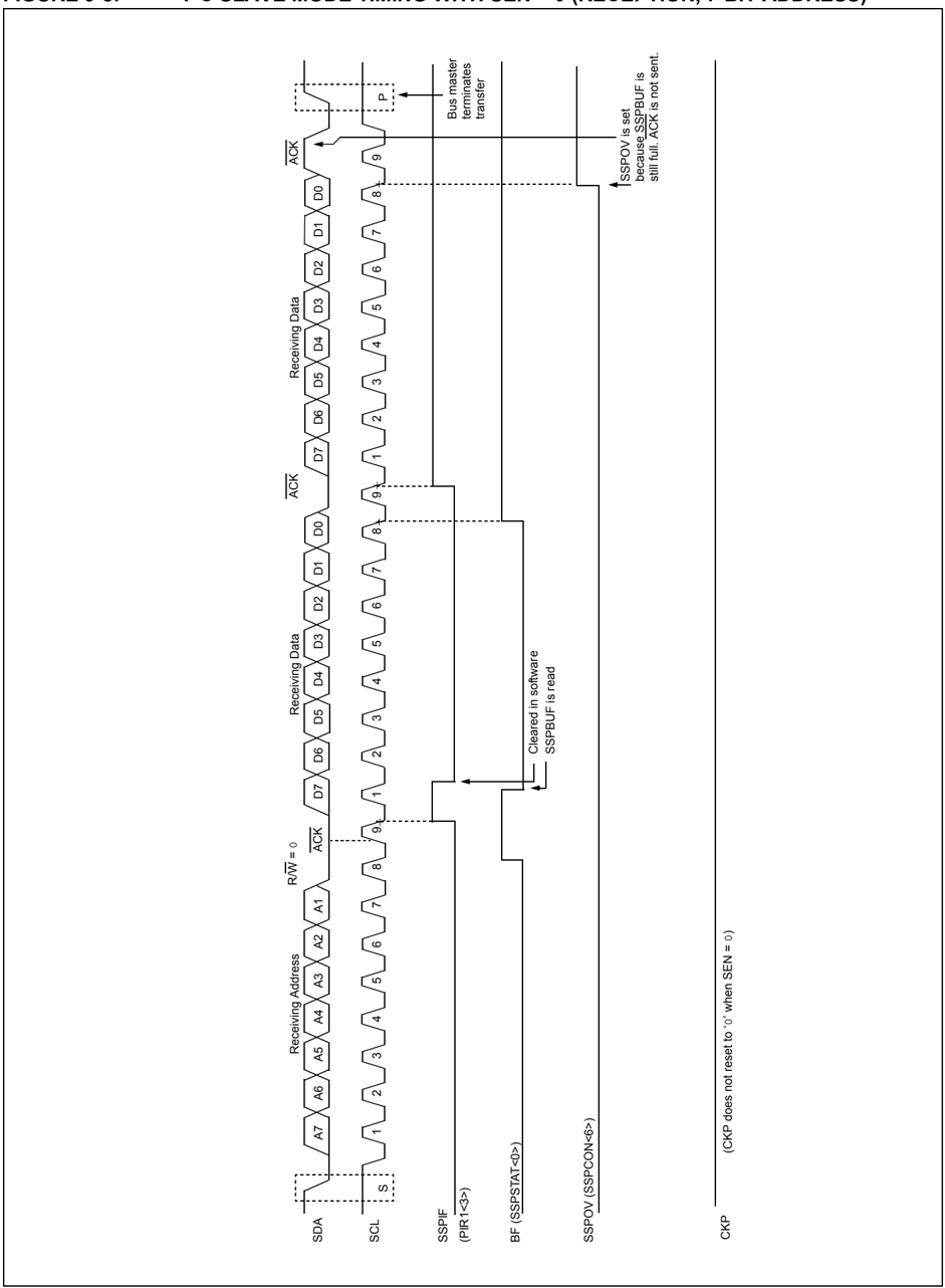
FIGURE 9-9: I²C SLAVE MODE TIMING (TRANSMISSION, 7-BIT ADDRESS)
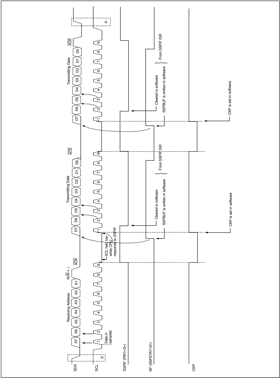
FIGURE 9-10: I²C SLAVE MODE TIMING WITH SEN = 0 (RECEPTION, 10-BIT ADDRESS)
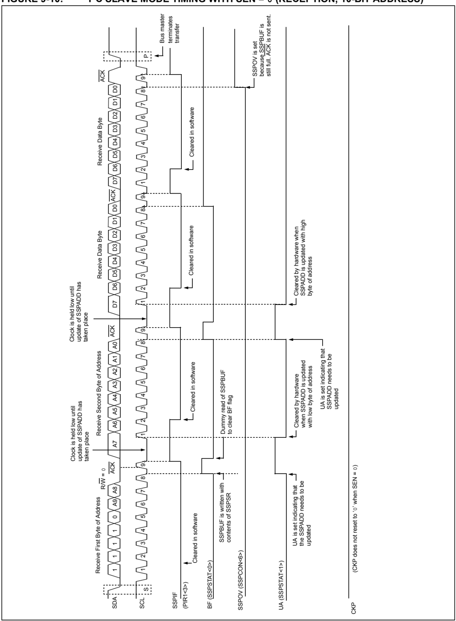
FIGURE 9-11: I²C SLAVE MODE TIMING (TRANSMISSION, 10-BIT ADDRESS)
9.4.4 CLOCK STRETCHING
Both 7 and 10-bit Slave modes implement automatic clock stretching during a transmit sequence.
The SEN bit (SSPCON2<0>) allows clock stretching to be enabled during receives. Setting SEN will cause the SCL pin to be held low at the end of each data receive sequence.
9.4.4.1 Clock Stretching for 7-bit Slave Receive Mode (SEN = 1)
In 7-bit Slave Receive mode, on the falling edge of the ninth clock at the end of the ACK sequence, if the BF bit is set, the CKP bit in the SSPCON register is automatically cleared, forcing the SCL output to be held low. The CKP bit being cleared to ‘0’ will assert the SCL line low. The CKP bit must be set in the user’s ISR before reception is allowed to continue. By holding the SCL line low, the user has time to service the ISR and read the contents of the SSPBUF before the master device can initiate another receive sequence. This will prevent buffer overruns from occurring (see Figure 9-13).
Note 1: If the user reads the contents of the SSPBUF before the falling edge of the ninth clock, thus clearing the BF bit, the CKP bit will not be cleared and clock stretching will not occur.
2: The CKP bit can be set in software regardless of the state of the BF bit. The user should be careful to clear the BF bit in the ISR before the next receive sequence in order to prevent an overflow condition.
9.4.4.2 Clock Stretching for 10-bit Slave Receive Mode (SEN = 1)
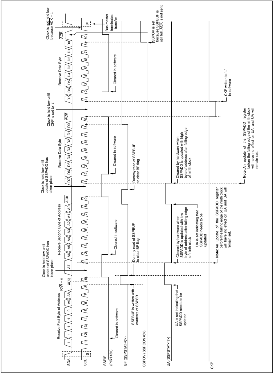
In 10-bit Slave Receive mode, during the address sequence, clock stretching automatically takes place but CKP is not cleared. During this time, if the UA bit is set after the ninth clock, clock stretching is initiated. The UA bit is set after receiving the upper byte of the 10-bit address and following the receive of the second byte of the 10-bit address, with the R/W bit cleared to ‘0’. The release of the clock line occurs upon updating SSPADD. Clock stretching will occur on each data receive sequence as described in 7-bit mode.
Note: If the user polls the UA bit and clears it by updating the SSPADD register before the falling edge of the ninth clock occurs and if the user hasn’t cleared the BF bit by reading the SSPBUF register before that time, then the CKP bit will still NOT be asserted low. Clock stretching, on the basis of the state of the BF bit, only occurs during a data sequence, not an address sequence.
9.4.4.3 Clock Stretching for 7-bit Slave Transmit Mode
7-bit Slave Transmit mode implements clock stretching by clearing the CKP bit after the falling edge of the ninth clock, if the BF bit is clear. This occurs regardless of the state of the SEN bit.
The user’s ISR must set the CKP bit before transmission is allowed to continue. By holding the SCL line low, the user has time to service the ISR and load the contents of the SSPBUF before the master device can initiate another transmit sequence (see Figure 9-9).
Note 1: If the user loads the contents of SSPBUF, setting the BF bit before the falling edge of the ninth clock, the CKP bit will not be cleared and clock stretching will not occur.
2: The CKP bit can be set in software regardless of the state of the BF bit.
9.4.4.4 Clock Stretching for 10-bit Slave Transmit Mode
In 10-bit Slave Transmit mode, clock stretching is controlled during the first two address sequences by the state of the UA bit, just as it is in 10-bit Slave Receive mode. The first two addresses are followed by a third address sequence, which contains the high order bits of the 10-bit address and the R/W bit set to ‘1’. After the third address sequence is performed, the UA bit is not set, the module is now configured in Transmit mode and clock stretching is controlled by the BF flag as in 7-bit Slave Transmit mode (see Figure 9-11).
9.4.4.5 Clock Synchronization and the CKP Bit
When the CKP bit is cleared, the SCL output is forced to '0'; however, setting the CKP bit will not assert the SCL output low until the SCL output is already sampled low. Therefore, the CKP bit will not assert the SCL line until an external I²C master device has already asserted the SCL line. The SCL output will remain low until the CKP bit is set and all other devices on the I²C bus have deasserted SCL. This ensures that a write to the CKP bit will not violate the minimum high time requirement for SCL (see Figure 9-12).
FIGURE 9-12: CLOCK SYNCHRONIZATION TIMING
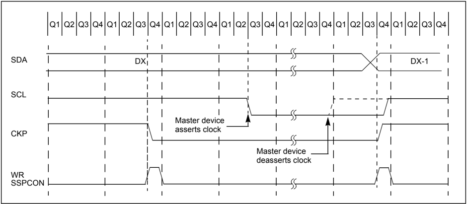
FIGURE 9-13: I²C SLAVE MODE TIMING WITH SEN = 1 (RECEPTION, 7-BIT ADDRESS)
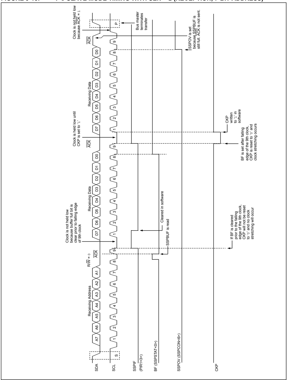
FIGURE 9-14: I²C SLAVE MODE TIMING SEN = 1 (RECEPTION, 10-BIT ADDRESS)
9.4.5 GENERAL CALL ADDRESS SUPPORT
The addressing procedure for the I$^2$C bus is such that the first byte after the Start condition usually determines which device will be the slave addressed by the master. The exception is the general call address which can address all devices. When this address is used, all devices should, in theory, respond with an Acknowledge.
The general call address is one of eight addresses reserved for specific purposes by the I$^2$C protocol. It consists of all '0's with R/\overlineW = 0.
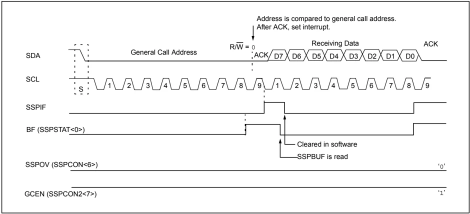
The general call address is recognized when the General Call Enable bit (GCEN) is enabled (SSPCON2<7> set). Following a Start bit detect, 8 bits are shifted into the SSPSR and the address is compared against the SSPADD. It is also compared to the general call address and fixed in hardware.
If the general call address matches, the SSPSR is transferred to the SSPBUF, the BF flag bit is set (eighth bit) and on the falling edge of the ninth bit (\overlineACK bit), the SSPIF interrupt flag bit is set.
When the interrupt is serviced, the source for the interrupt can be checked by reading the contents of the SSPBUF. The value can be used to determine if the address was device specific or a general call address.
In 10-bit mode, the SSPADD is required to be updated for the second half of the address to match and the UA bit is set (SSPSTAT<1>). If the general call address is sampled when the GCEN bit is set, while the slave is configured in 10-bit Address mode, then the second half of the address is not necessary, the UA bit will not be set and the slave will begin receiving data after the Acknowledge (Figure 9-15).
FIGURE 9-15: SLAVE MODE GENERAL CALL ADDRESS SEQUENCE (7 OR 10-BIT ADDRESS MODE)
9.4.6 MASTER MODE
Master mode is enabled by setting and clearing the appropriate SSPM bits in SSPCON and by setting the SSPEN bit. In Master mode, the SCL and SDA lines are manipulated by the MSSP hardware.
Master mode of operation is supported by interrupt generation on the detection of the Start and Stop conditions. The Stop (P) and Start (S) bits are cleared from a Reset or when the MSSP module is disabled. Control of the I²C bus may be taken when the P bit is set or the bus is Idle, with both the S and P bits clear.
In Firmware Controlled Master mode, user code conducts all I²C bus operations based on Start and Stop bit conditions.
Once Master mode is enabled, the user has six options.
- Assert a Start condition on SDA and SCL.
- Assert a Repeated Start condition on SDA and SCL.
- Write to the SSPBUF register, initiating transmission of data/address.
- Configure the I²C port to receive data.
- Generate an Acknowledge condition at the end of a received byte of data.
- Generate a Stop condition on SDA and SCL.
Note: The MSSP module, when configured in I²C Master mode, does not allow queueing of events. For instance, the user is not allowed to initiate a Start condition and immediately write the SSPBUF register to initiate transmission before the Start condition is complete. In this case, the SSPBUF will not be written to and the WCOL bit will be set, indicating that a write to the SSPBUF did not occur.
The following events will cause SSP Interrupt Flag bit, SSPIF, to be set (SSP interrupt if enabled):
• Start condition
• Stop condition
• Data transfer byte transmitted/received
• Acknowledge transmit
• Repeated Start
FIGURE 9-16: MSSP BLOCK DIAGRAM (I²C MASTER MODE)
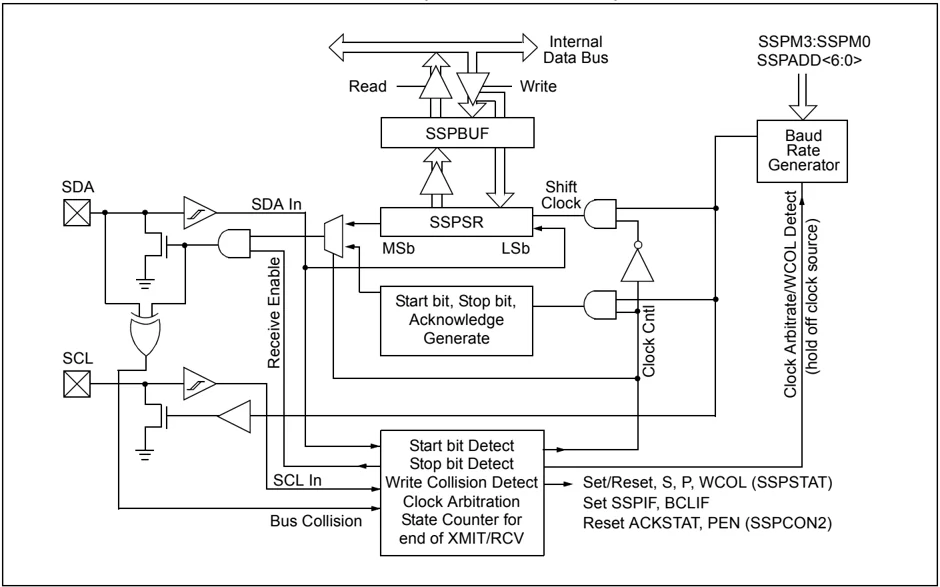
9.4.6.1 I²C Master Mode Operation
The master device generates all of the serial clock pulses and the Start and Stop conditions. A transfer is ended with a Stop condition or with a Repeated Start condition. Since the Repeated Start condition is also the beginning of the next serial transfer, the I²C bus will not be released.
In Master Transmitter mode, serial data is output through SDA while SCL outputs the serial clock. The first byte transmitted contains the slave address of the receiving device (7 bits) and the Read/Write (R/W) bit. In this case, the R/W bit will be logic '0'. Serial data is transmitted 8 bits at a time. After each byte is transmitted, an Acknowledge bit is received. Start and Stop conditions are output to indicate the beginning and the end of a serial transfer.
In Master Receive mode, the first byte transmitted contains the slave address of the transmitting device (7 bits) and the R/W bit. In this case, the R/W bit will be logic '1'. Thus, the first byte transmitted is a 7-bit slave address followed by a '1' to indicate the receive bit. Serial data is received via SDA while SCL outputs the serial clock. Serial data is received 8 bits at a time. After each byte is received, an Acknowledge bit is transmitted. Start and Stop conditions indicate the beginning and end of transmission.
The baud rate generator used for the SPI mode operation is used to set the SCL clock frequency for either 100 kHz, 400 kHz or 1 MHz I²C operation. See Section 9.4.7 "Baud Rate Generator" for more detail.
A typical transmit sequence would go as follows:
- The user generates a Start condition by setting the Start Enable bit, SEN (SSPCON2<0>).
- SSPIF is set. The MSSP module will wait the required Start time before any other operation takes place.
- The user loads the SSPBUF with the slave address to transmit.
- Address is shifted out the SDA pin until all 8 bits are transmitted.
- The MSSP module shifts in the ACK bit from the slave device and writes its value into the SSPCON2 register (SSPCON2<6>).
- The MSSP module generates an interrupt at the end of the ninth clock cycle by setting the SSPIF bit.
- The user loads the SSPBUF with eight bits of data.
- Data is shifted out the SDA pin until all 8 bits are transmitted.
- The MSSP module shifts in the ACK bit from the slave device and writes its value into the SSPCON2 register (SSPCON2<6>).
- The MSSP module generates an interrupt at the end of the ninth clock cycle by setting the SSPIF bit.
- The user generates a Stop condition by setting the Stop Enable bit, PEN (SSPCON2<2>).
- Interrupt is generated once the Stop condition is complete.
DS39582C-page 96 © 2001-2013 Microchip Technology Inc.
9.4.7 BAUD RATE GENERATOR
In I²C Master mode, the Baud Rate Generator (BRG) reload value is placed in the lower 7 bits of the SSPADD register (Figure 9-17). When a write occurs to SSPBUF, the Baud Rate Generator will automatically begin counting. The BRG counts down to 0 and stops until another reload has taken place. The BRG count is decremented twice per instruction cycle (TCY) on the Q2 and Q4 clocks. In I²C Master mode, the BRG is reloaded automatically.
Once the given operation is complete (i.e., transmission of the last data bit is followed by \overlineACK), the internal clock will automatically stop counting and the SCL pin will remain in its last state.
Table 9-3 demonstrates clock rates based on instruction cycles and the BRG value loaded into SSPADD.
FIGURE 9-17: BAUD RATE GENERATOR BLOCK DIAGRAM
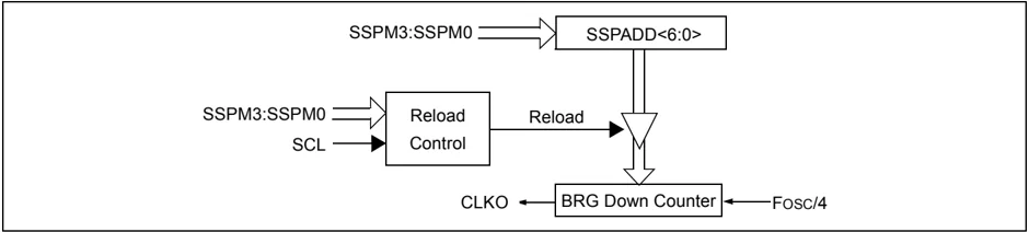
TABLE 9-3: I²C CLOCK RATE W/BRG
Note 1: The I²C interface does not conform to the 400 kHz I²C specification (which applies to rates greater than 100 kHz) in all details, but may be used with care where higher rates are required by the application.
9.4.7.1 Clock Arbitration
Clock arbitration occurs when the master, during any receive, transmit or Repeated Start/Stop condition, deasserts the SCL pin (SCL allowed to float high). When the SCL pin is allowed to float high, the Baud Rate Generator (BRG) is suspended from counting until the SCL pin is actually sampled high. When the SCL pin is sampled high, the Baud Rate Generator is reloaded with the contents of SSPADD<6:0> and begins counting. This ensures that the SCL high time will always be at least one BRG rollover count, in the event that the clock is held low by an external device (Figure 9-17).
FIGURE 9-18: BAUD RATE GENERATOR TIMING WITH CLOCK ARBITRATION
 SDA DX DX-1
SCL deasserted but slave holds SCL low (clock arbitration) SCL allowed to transition high SCL
BRG decrements on Q2 and Q4 cycles BRG Value 03h 02h 01h 00h (hold off) 03h 02h
SCL is sampled high, reload takes place and BRG starts its count BRG Reload
DS39582C-page 98 © 2001-2013 Microchip Technology Inc.
9.4.8 I²C MASTER MODE START CONDITION TIMING
To initiate a Start condition, the user sets the Start condition enable bit, SEN (SSPCON2<0>). If the SDA and SCL pins are sampled high, the Baud Rate Generator is reloaded with the contents of SSPADD<6:0> and starts its count. If SCL and SDA are both sampled high when the Baud Rate Generator times out ($T_{BRG}$), the SDA pin is driven low. The action of the SDA being driven low, while SCL is high, is the Start condition and causes the S bit (SSPSTAT<3>) to be set. Following this, the Baud Rate Generator is reloaded with the contents of SSPADD<6:0> and resumes its count. When the Baud Rate Generator times out ($T_{BRG}$), the SEN bit (SSPCON2<0>) will be automatically cleared by hardware, the Baud Rate Generator is suspended, leaving the SDA line held low and the Start condition is complete.
Note: If at the beginning of the Start condition, the SDA and SCL pins are already sampled low, or if during the Start condition, the SCL line is sampled low before the SDA line is driven low, a bus collision occurs, the Bus Collision Interrupt Flag (BCLIF) is set, the Start condition is aborted and the I²C module is reset into its Idle state.
9.4.8.1 WCOL Status Flag
If the user writes the SSPBUF when a Start sequence is in progress, the WCOL is set and the contents of the buffer are unchanged (the write doesn't occur).
Note: Because queueing of events is not allowed, writing to the lower 5 bits of SSPCON2 is disabled until the Start condition is complete.
FIGURE 9-19: FIRST START BIT TIMING
 Write to SEN bit occurs here
Set S bit (SSPSTAT<3>)
SDA = 1,
SCL = 1
At completion of Start bit,
hardware clears SEN bit
and sets SSPIF bit
| \leftarrow T_BRG \rightarrow | \leftarrow T_BRG \rightarrow |
Write to SSPBUF occurs here
SDA
1st Bit
2nd Bit
SCL
| \leftarrow T_BRG \rightarrow |
| \leftarrow T_BRG \rightarrow |
S
9.4.9 I²C MASTER MODE REPEATED START CONDITION TIMING
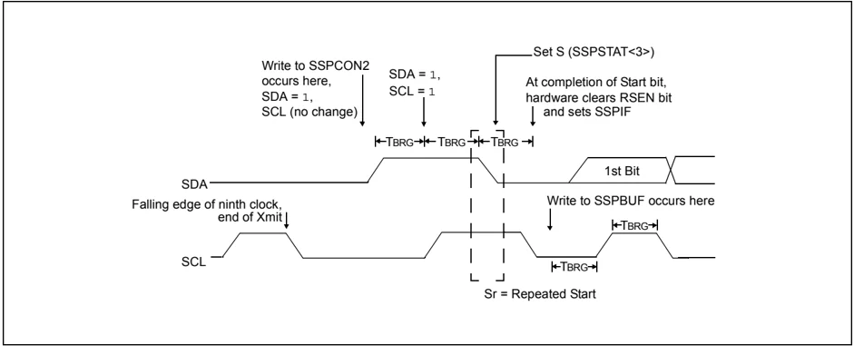
A Repeated Start condition occurs when the RSEN bit (SSPCON2<1>) is programmed high and the I²C logic module is in the Idle state. When the RSEN bit is set, the SCL pin is asserted low. When the SCL pin is sampled low, the Baud Rate Generator is loaded with the contents of SSPADD<5:0> and begins counting. The SDA pin is released (brought high) for one Baud Rate Generator count (TBRG). When the Baud Rate Generator times out, if SDA is sampled high, the SCL pin will be deasserted (brought high). When SCL is sampled high, the Baud Rate Generator is reloaded with the contents of SSPADD<6:0> and begins counting. SDA and SCL must be sampled high for one TBRG. This action is then followed by assertion of the SDA pin (SDA = 0) for one TBRG while SCL is high. Following this, the RSEN bit (SSPCON2<1>) will be automatically cleared and the Baud Rate Generator will not be reloaded, leaving the SDA pin held low. As soon as a Start condition is detected on the SDA and SCL pins, the S bit (SSPSTAT<3>) will be set. The SSPIF bit will not be set until the Baud Rate Generator has timed out.
Note 1: If RSEN is programmed while any other event is in progress, it will not take effect. 2: A bus collision during the Repeated Start condition occurs if:
- SDA is sampled low when SCL goes from low to high.
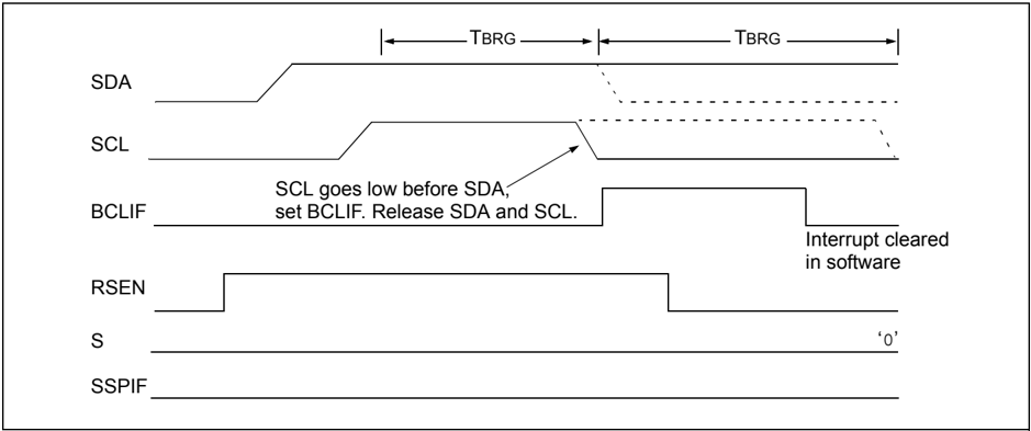
- SCL goes low before SDA is asserted low. This may indicate that another master is attempting to transmit a data '1'.
Immediately following the SSPIF bit getting set, the user may write the SSPBUF with the 7-bit address in 7-bit mode or the default first address in 10-bit mode. After the first eight bits are transmitted and an ACK is received, the user may then transmit an additional eight bits of address (10-bit mode) or eight bits of data (7-bit mode).
9.4.9.1 WCOL Status Flag
If the user writes the SSPBUF when a Repeated Start sequence is in progress, the WCOL is set and the contents of the buffer are unchanged (the write doesn't occur).
Note: Because queueing of events is not allowed, writing of the lower 5 bits of SSPCON2 is disabled until the Repeated Start condition is complete.
FIGURE 9-20: REPEAT START CONDITION WAVEFORM
9.4.10 I²C MASTER MODE TRANSMISSION
Transmission of a data byte, a 7-bit address or the other half of a 10-bit address is accomplished by simply writing a value to the SSPBUF register. This action will set the Buffer Full flag bit, BF, and allow the Baud Rate Generator to begin counting and start the next transmission. Each bit of address/data will be shifted out onto the SDA pin after the falling edge of SCL is asserted (see data hold time specification, parameter #106). SCL is held low for one Baud Rate Generator rollover count (TBRG). Data should be valid before SCL is released high (see data setup time specification, parameter #107). When the SCL pin is released high, it is held that way for TBRG. The data on the SDA pin must remain stable for that duration and some hold time after the next falling edge of SCL. After the eighth bit is shifted out (the falling edge of the eighth clock), the BF flag is cleared and the master releases SDA. This allows the slave device being addressed to respond with an ACK bit during the ninth bit time, if an address match occurred or if data was received properly. The status of ACK is written into the ACKDT bit on the falling edge of the ninth clock. If the master receives an Acknowledge, the Acknowledge Status bit, ACKSTAT, is cleared. If not, the bit is set. After the ninth clock, the SSPIF bit is set and the master clock (Baud Rate Generator) is suspended until the next data byte is loaded into the SSPBUF, leaving SCL low and SDA unchanged (Figure 9-21).
After the write to the SSPBUF, each bit of address will be shifted out on the falling edge of SCL, until all seven address bits and the R/W bit are completed. On the falling edge of the eighth clock, the master will deassert the SDA pin, allowing the slave to respond with an Acknowledge. On the falling edge of the ninth clock, the master will sample the SDA pin to see if the address was recognized by a slave. The status of the ACK bit is loaded into the ACKSTAT status bit (SSPCON2<6>). Following the falling edge of the ninth clock transmission of the address, the SSPIF is set, the BF flag is cleared and the Baud Rate Generator is turned off until another write to the SSPBUF takes place, holding SCL low and allowing SDA to float.
9.4.10.1 BF Status Flag
In Transmit mode, the BF bit (SSPSTAT<0>) is set when the CPU writes to SSPBUF and is cleared when all eight bits are shifted out.
9.4.10.2 WCOL Status Flag
If the user writes the SSPBUF when a transmit is already in progress (i.e., SSPSR is still shifting out a data byte), the WCOL is set and the contents of the buffer are unchanged (the write doesn't occur).
WCOL must be cleared in software.
9.4.10.3 ACKSTAT Status Flag
In Transmit mode, the ACKSTAT bit (SSPCON2<6>) is cleared when the slave has sent an Acknowledge (\overlineACK = 0) and is set when the slave does Not Acknowledge (\overlineACK = 1). A slave sends an Acknowledge when it has recognized its address (including a general call) or when the slave has properly received its data.
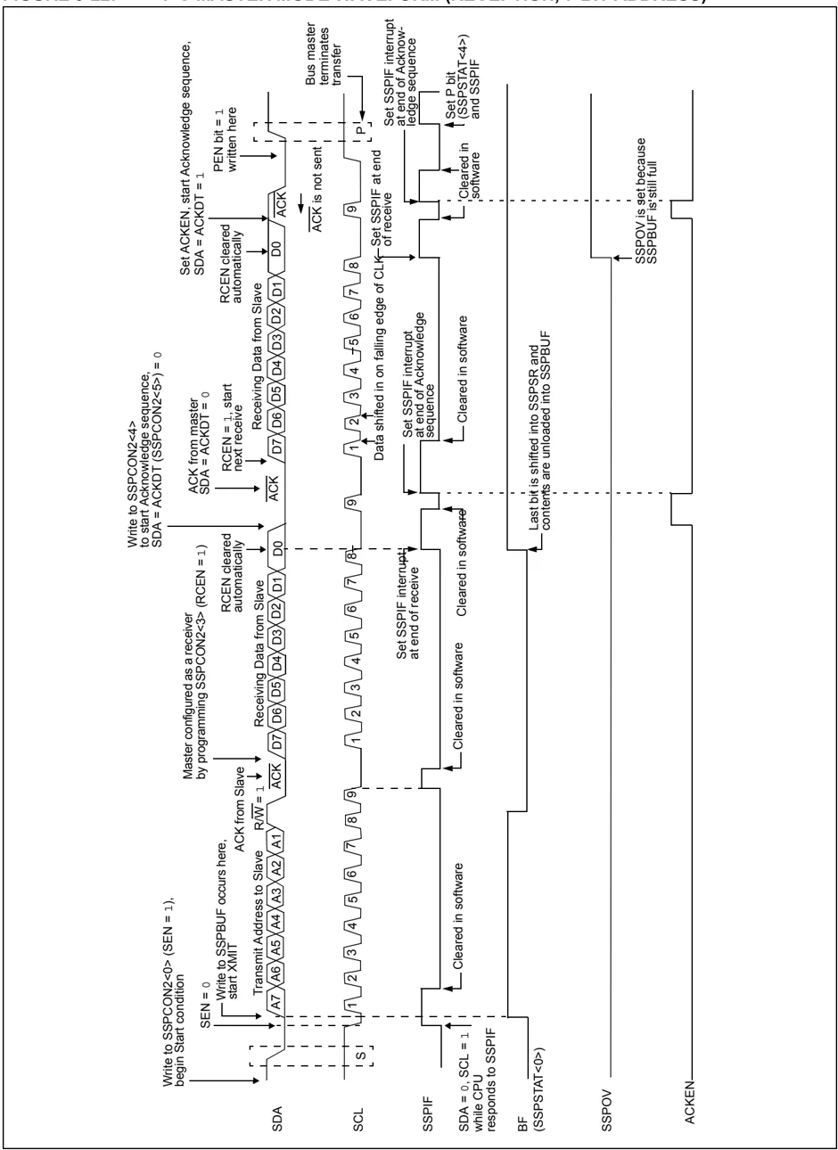
9.4.11 I²C MASTER MODE RECEPTION
Master mode reception is enabled by programming the Receive Enable bit, RCEN (SSPCON2<3>).
Note: The MSSP module must be in an Idle state before the RCEN bit is set or the RCEN bit will be disregarded.
The Baud Rate Generator begins counting and on each rollover, the state of the SCL pin changes (high to low/low to high) and data is shifted into the SSPSR. After the falling edge of the eighth clock, the receive enable flag is automatically cleared, the contents of the SSPSR are loaded into the SSPBUF, the BF flag bit is set, the SSPIF flag bit is set and the Baud Rate Generator is suspended from counting, holding SCL low. The MSSP is now in Idle state, awaiting the next command. When the buffer is read by the CPU, the BF flag bit is automatically cleared. The user can then send an Acknowledge bit at the end of reception by setting the Acknowledge Sequence Enable bit, ACKEN (SSPCON2<4>).
9.4.11.1 BF Status Flag
In receive operation, the BF bit is set when an address or data byte is loaded into SSPBUF from SSPSR. It is cleared when the SSPBUF register is read.
9.4.11.2 SSPOV Status Flag
In receive operation, the SSPOV bit is set when 8 bits are received into the SSPSR and the BF flag bit is already set from a previous reception.
9.4.11.3 WCOL Status Flag
If the user writes the SSPBUF when a receive is already in progress (i.e., SSPSR is still shifting in a data byte), the WCOL bit is set and the contents of the buffer are unchanged (the write doesn't occur).
FIGURE 9-21: I²C MASTER MODE WAVEFORM (TRANSMISSION, 7 OR 10-BIT ADDRESS)
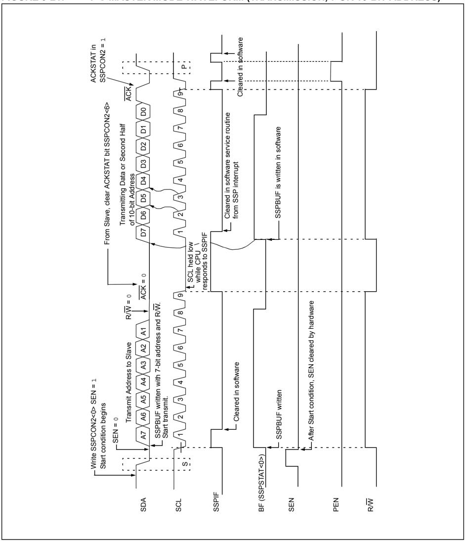
FIGURE 9-22: I²C MASTER MODE WAVEFORM (RECEPTION, 7-BIT ADDRESS)
9.4.12 ACKNOWLEDGE SEQUENCE TIMING
An Acknowledge sequence is enabled by setting the Acknowledge Sequence Enable bit, ACKEN (SSPCON2<4>). When this bit is set, the SCL pin is pulled low and the contents of the Acknowledge data bit are presented on the SDA pin. If the user wishes to generate an Acknowledge, then the ACKDT bit should be cleared. If not, the user should set the ACKDT bit before starting an Acknowledge sequence. The Baud Rate Generator then counts for one rollover period (TBRG) and the SCL pin is deasserted (pulled high). When the SCL pin is sampled high (clock arbitration), the Baud Rate Generator counts for TBRG. The SCL pin is then pulled low. Following this, the ACKEN bit is automatically cleared, the baud rate generator is turned off and the MSSP module then goes into Idle mode (Figure 9-23).
9.4.12.1 WCOL Status Flag
If the user writes the SSPBUF when an Acknowledge sequence is in progress, then WCOL is set and the contents of the buffer are unchanged (the write doesn't occur).
9.4.13 STOP CONDITION TIMING
A Stop bit is asserted on the SDA pin at the end of a receive/transmit by setting the Stop Sequence Enable bit, PEN (SSPCON2<2>). At the end of a receive/ transmit, the SCL line is held low after the falling edge of the ninth clock. When the PEN bit is set, the master will assert the SDA line low. When the SDA line is sampled low, the Baud Rate Generator is reloaded and counts down to 0. When the Baud Rate Generator times out, the SCL pin will be brought high and one TBRG (Baud Rate Generator rollover count) later, the SDA pin will be deasserted. When the SDA pin is sampled high while SCL is high, the P bit (SSPSTAT<4>) is set. A TBRG later, the PEN bit is cleared and the SSPIF bit is set (Figure 9-24).
9.4.13.1 WCOL Status Flag
If the user writes the SSPBUF when a Stop sequence is in progress, then the WCOL bit is set and the contents of the buffer are unchanged (the write doesn't occur).
FIGURE 9-23: ACKNOWLEDGE SEQUENCE WAVEFORM
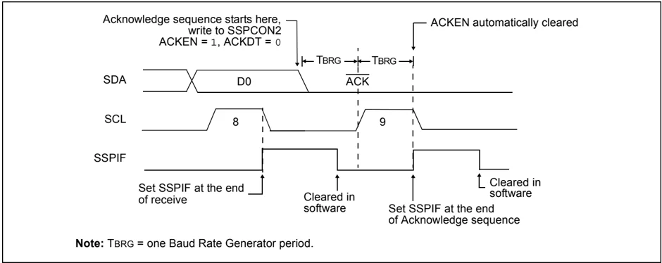
Note: TBRG = one Baud Rate Generator period.
FIGURE 9-24: STOP CONDITION RECEIVE OR TRANSMIT MODE
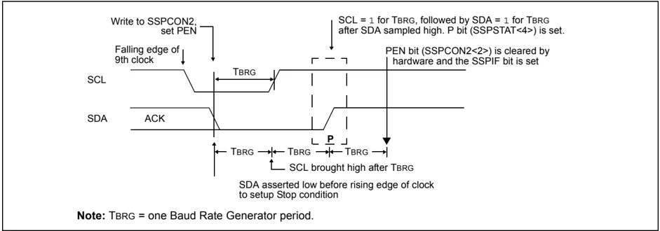
Note: TBRG = one Baud Rate Generator period.
9.4.14 SLEEP OPERATION
While in Sleep mode, the I$^2$C module can receive addresses or data and when an address match or complete byte transfer occurs, wake the processor from Sleep (if the MSSP interrupt is enabled).
9.4.15 EFFECT OF A RESET
A Reset disables the MSSP module and terminates the current transfer.
9.4.16 MULTI-MASTER MODE
In Multi-Master mode, the interrupt generation on the detection of the Start and Stop conditions allows the determination of when the bus is free. The Stop (P) and Start (S) bits are cleared from a Reset or when the MSSP module is disabled. Control of the I$^2$C bus may be taken when the P bit (SSPSTAT<4>) is set, or the bus is Idle, with both the S and P bits clear. When the bus is busy, enabling the SSP interrupt will generate the interrupt when the Stop condition occurs.
In multi-master operation, the SDA line must be monitored for arbitration to see if the signal level is at the expected output level. This check is performed in hardware with the result placed in the BCLIF bit.
The states where arbitration can be lost are:
- Address Transfer
- Data Transfer
- A Start Condition
- A Repeated Start Condition
- An Acknowledge Condition
9.4.17 MULTI-MASTER COMMUNICATION, BUS COLLISION AND BUS ARBITRATION
Multi-Master mode support is achieved by bus arbitration. When the master outputs address/data bits onto the SDA pin, arbitration takes place when the master outputs a '1' on SDA by letting SDA float high and another master asserts a '0'. When the SCL pin floats high, data should be stable. If the expected data on SDA is a '1' and the data sampled on the SDA pin = 0, then a bus collision has taken place. The master will set the Bus Collision Interrupt Flag, BCLIF, and reset the I$^2$C port to its Idle state (Figure 9-25).
If a transmit was in progress when the bus collision occurred, the transmission is halted, the BF flag is cleared, the SDA and SCL lines are deasserted and the SSPBUF can be written to. When the user services the bus collision Interrupt Service Routine and if the I$^2$C bus is free, the user can resume communication by asserting a Start condition.
If a Start, Repeated Start, Stop or Acknowledge condition was in progress when the bus collision occurred, the condition is aborted, the SDA and SCL lines are deasserted and the respective control bits in the SSPCON2 register are cleared. When the user services the bus collision Interrupt Service Routine and if the I$^2$C bus is free, the user can resume communication by asserting a Start condition.
The Master will continue to monitor the SDA and SCL pins. If a Stop condition occurs, the SSPIF bit will be set.
A write to the SSPBUF will start the transmission of data at the first data bit regardless of where the transmitter left off when the bus collision occurred.
In Multi-Master mode, the interrupt generation on the detection of Start and Stop conditions allows the determination of when the bus is free. Control of the I$^2$C bus can be taken when the P bit is set in the SSPSTAT register or the bus is Idle and the S and P bits are cleared.
FIGURE 9-25: BUS COLLISION TIMING FOR TRANSMIT AND ACKNOWLEDGE
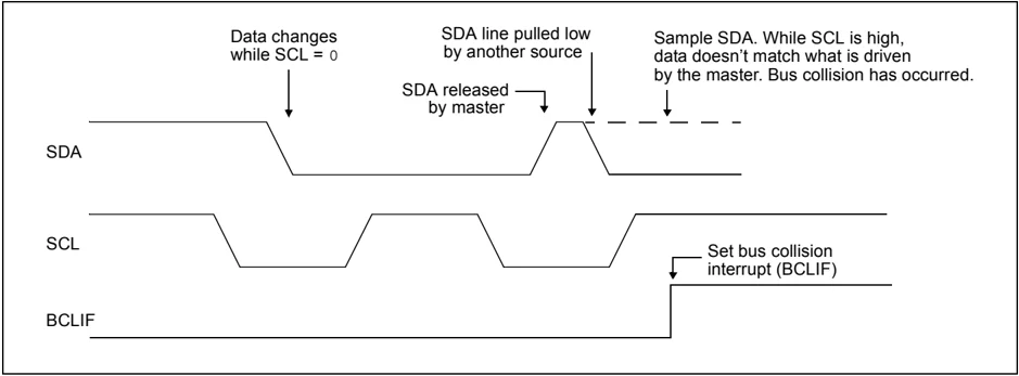
9.4.17.1 Bus Collision During a Start Condition
During a Start condition, a bus collision occurs if: a) SDA or SCL are sampled low at the beginning of the Start condition (Figure 9-26). b) SCL is sampled low before SDA is asserted low (Figure 9-27).
During a Start condition, both the SDA and the SCL pins are monitored.
If the SDA pin is already low, or the SCL pin is already low, then all of the following occur:
- the Start condition is aborted,
- the BCLIF flag is set and
- the MSSP module is reset to its Idle state (Figure 9-26).
The Start condition begins with the SDA and SCL pins deasserted. When the SDA pin is sampled high, the Baud Rate Generator is loaded from SSPADD<6:0> and counts down to 0. If the SCL pin is sampled low while SDA is high, a bus collision occurs because it is assumed that another master is attempting to drive a data '1' during the Start condition.
If the SDA pin is sampled low during this count, the BRG is reset and the SDA line is asserted early (Figure 9-28). If, however, a '1' is sampled on the SDA pin, the SDA pin is asserted low at the end of the BRG count. The Baud Rate Generator is then reloaded and counts down to 0 and during this time, if the SCL pin is sampled as '0', a bus collision does not occur. At the end of the BRG count, the SCL pin is asserted low.
Note: The reason that bus collision is not a factor during a Start condition is that no two bus masters can assert a Start condition at the exact same time. Therefore, one master will always assert SDA before the other. This condition does not cause a bus collision because the two masters must be allowed to arbitrate the first address following the Start condition. If the address is the same, arbitration must be allowed to continue into the data portion, Repeated Start or Stop conditions.
FIGURE 9-26: BUS COLLISION DURING START CONDITION (SDA ONLY)
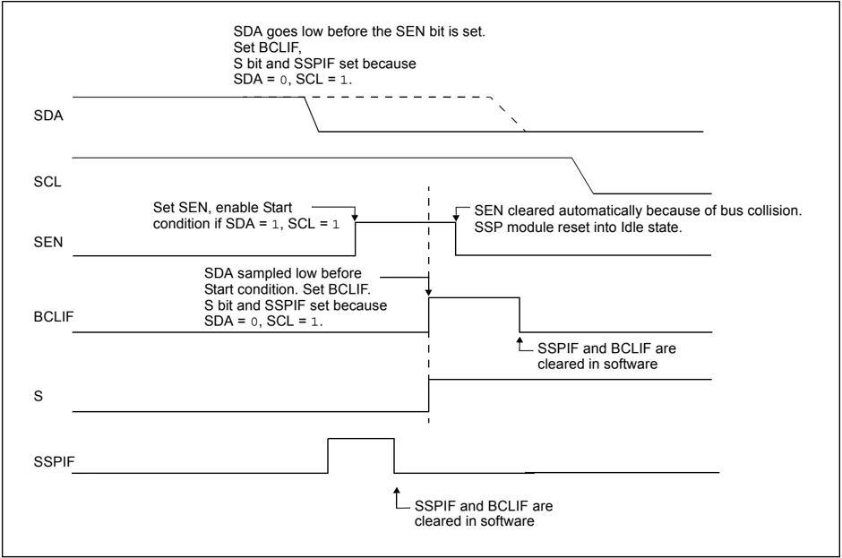
FIGURE 9-27: BUS COLLISION DURING START CONDITION (SCL = 0)
 SDA = 0, SCL = 1
|← TBRG →|← TBRG →|
SDA
SCL
Set SEN, enable Start
sequence if SDA = 1, SCL = 1
SEN
SCL = 0 before SDA = 0,
bus collision occurs. Set BCLIF.
SCL = 0 before BRG time-out,
bus collision occurs. Set BCLIF.
BCLIF
Interrupt cleared
in software
S
‘0’
‘0’
SSPIF
‘0’
‘0’
FIGURE 9-28: BRG RESET DUE TO SDA ARBITRATION DURING START CONDITION
 SDA = 0, SCL = 1
Less than TBRG
|← TBRG →|
Set S
Set SSPIF
SDA pulled low by other master.
Reset BRG and assert SDA.
SDA
SCL
S
SCL pulled low after BRG
time-out
SEN
Set SEN, enable Start
sequence if SDA = 1, SCL = 1
BCLIF
‘0’
S
SSPIF
SDA = 0, SCL = 1,
set SSPIF
Interrupts cleared
in software
9.4.17.2 Bus Collision During a Repeated Start Condition
During a Repeated Start condition, a bus collision occurs if:
a) A low level is sampled on SDA when SCL goes from low level to high level. b) SCL goes low before SDA is asserted low, indicating that another master is attempting to transmit a data '1'.
When the user deasserts SDA and the pin is allowed to float high, the BRG is loaded with SSPADD<6:0> and counts down to 0. The SCL pin is then deasserted and when sampled high, the SDA pin is sampled.
If SDA is low, a bus collision has occurred (i.e., another master is attempting to transmit a data '0', see Figure 9-29). If SDA is sampled high, the BRG is reloaded and begins counting. If SDA goes from high to low before the BRG times out, no bus collision occurs because no two masters can assert SDA at exactly the same time.
If SCL goes from high to low before the BRG times out and SDA has not already been asserted, a bus collision occurs. In this case, another master is attempting to transmit a data '1' during the Repeated Start condition (Figure 9-30).
If at the end of the BRG time-out, both SCL and SDA are still high, the SDA pin is driven low and the BRG is reloaded and begins counting. At the end of the count, regardless of the status of the SCL pin, the SCL pin is driven low and the Repeated Start condition is complete.
FIGURE 9-29: BUS COLLISION DURING A REPEATED START CONDITION (CASE 1)
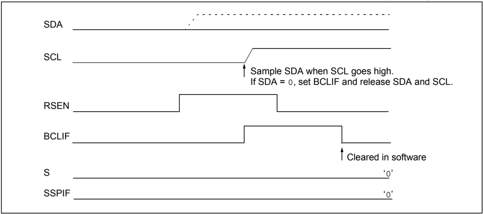
FIGURE 9-30: BUS COLLISION DURING REPEATED START CONDITION (CASE 2)
9.4.17.3 Bus Collision During a Stop Condition
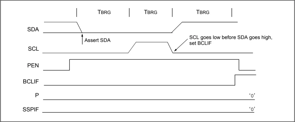
Bus collision occurs during a Stop condition if: a) After the SDA pin has been deasserted and allowed to float high, SDA is sampled low after the BRG has timed out. b) After the SCL pin is deasserted, SCL is sampled low before SDA goes high.
The Stop condition begins with SDA asserted low. When SDA is sampled low, the SCL pin is allowed to float. When the pin is sampled high (clock arbitration), the Baud Rate Generator is loaded with SSPADD<6:0> and counts down to 0. After the BRG times out, SDA is sampled. If SDA is sampled low, a bus collision has occurred. This is due to another master attempting to drive a data '0' (Figure 9-31). If the SCL pin is sampled low before SDA is allowed to float high, a bus collision occurs. This is another case of another master attempting to drive a data '0' (Figure 9-32).
FIGURE 9-31: BUS COLLISION DURING A STOP CONDITION (CASE 1)
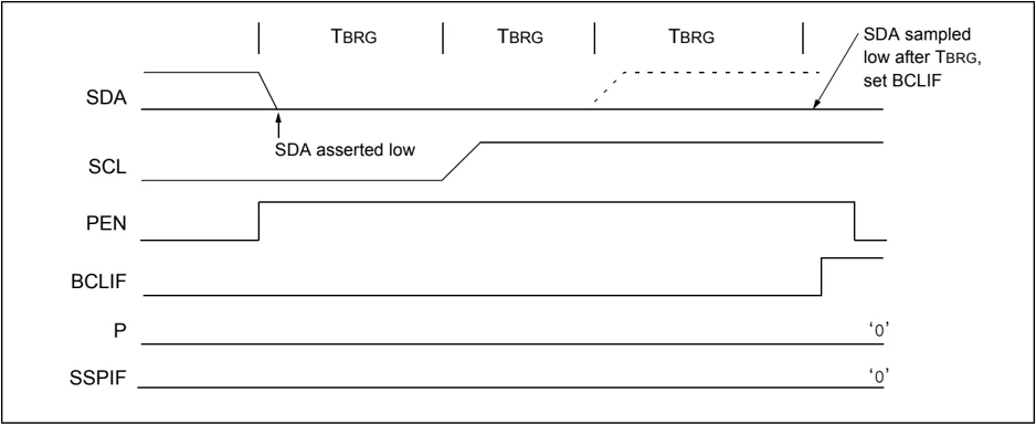
FIGURE 9-32: BUS COLLISION DURING A STOP CONDITION (CASE 2)