11.0 ANALOG-TO-DIGITAL CONVERTER (A/D) MODULE
The Analog-to-Digital (A/D) Converter module has five inputs for the 28-pin devices and eight for the 40/44-pin devices.
The conversion of an analog input signal results in a corresponding 10-bit digital number. The A/D module has high and low-voltage reference input that is software selectable to some combination of VDD, VSS, RA2 or RA3.
The A/D converter has a unique feature of being able to operate while the device is in Sleep mode. To operate in Sleep, the A/D clock must be derived from the A/D’s internal RC oscillator.
The A/D module has four registers. These registers are:
- A/D Result High Register (ADRESH)
- A/D Result Low Register (ADRESL)
- A/D Control Register 0 (ADCON0)
- A/D Control Register 1 (ADCON1)
The ADCON0 register, shown in Register 11-1, controls the operation of the A/D module. The ADCON1 register, shown in Register 11-2, configures the functions of the port pins. The port pins can be configured as analog inputs (RA3 can also be the voltage reference) or as digital I/O.
Additional information on using the A/D module can be found in the PIC® Mid-Range MCU Family Reference Manual (DS33023).
REGISTER 11-1: ADCON0 REGISTER (ADDRESS 1Fh)
| R/W-0 | R/W-0 | R/W-0 | R/W-0 | R/W-0 | R/W-0 | U-0 | R/W-0 |
|---|---|---|---|---|---|---|---|
| ADCS1 | ADCS0 | CHS2 | CHS1 | CHS0 | GO/DONE | — | ADON |
| bit 7 | bit 0 |
bit 7-6 ADCS1:ADCS0: A/D Conversion Clock Select bits (ADCON0 bits in bold)
| ADCON1 <ADCS2> | ADCON0 ADCS1:ADCS0 | Clock Conversion |
|---|---|---|
| 0 | 00 | Fosc/2 |
| 0 | 01 | Fosc/8 |
| 0 | 10 | Fosc/32 |
| 0 | 11 | FRC (clock derived from the internal A/D RC oscillator) |
| 1 | 00 | Fosc/4 |
| 1 | 01 | Fosc/16 |
| 1 | 10 | Fosc/64 |
| 1 | 11 | FRC (clock derived from the internal A/D RC oscillator) |
bit 5-3 CHS2:CHS0: Analog Channel Select bits
000 = Channel 0 (AN0)
001 = Channel 1 (AN1)
010 = Channel 2 (AN2)
011 = Channel 3 (AN3)
100 = Channel 4 (AN4)
101 = Channel 5 (AN5)
110 = Channel 6 (AN6)
111 = Channel 7 (AN7)
Note: The PIC16F873A/876A devices only implement A/D channels 0 through 4; the unimplemented selections are reserved. Do not select any unimplemented channels with these devices.
bit 2 GO/DONE: A/D Conversion Status bit
When ADON = 1:
1 = A/D conversion in progress (setting this bit starts the A/D conversion which is automatically cleared by hardware when the A/D conversion is complete)
0 = A/D conversion not in progress
bit 1 Unimplemented: Read as ‘0’
bit 0 ADON: A/D On bit
1 = A/D converter module is powered up
0 = A/D converter module is shut-off and consumes no operating current
Legend:
R = Readable bit
W = Writable bit
U = Unimplemented bit, read as ‘0’
-n = Value at POR
‘1’ = Bit is set
‘0’ = Bit is cleared
x = Bit is unknown
REGISTER 11-2: ADCON1 REGISTER (ADDRESS 9Fh)
| R/W-0 | R/W-0 | U-0 | U-0 | R/W-0 | R/W-0 | R/W-0 | R/W-0 |
|---|---|---|---|---|---|---|---|
| ADFM | ADCS2 | — | — | PCFG3 | PCFG2 | PCFG1 | PCFG0 |
| bit 7 | bit 0 |
bit 7 ADFM: A/D Result Format Select bit
- 1 = Right justified. Six (6) Most Significant bits of ADRESH are read as ‘0’.
- 0 = Left justified. Six (6) Least Significant bits of ADRESL are read as ‘0’.
bit 6 ADCS2: A/D Conversion Clock Select bit (ADCON1 bits in shaded area and in bold)
| ADCON1 <ADCS2> | ADCON0 ADCS1:ADCS0 | Clock Conversion |
|---|---|---|
| 0 | 00 | FOSC/2 |
| 0 | 01 | FOSC/8 |
| 0 | 10 | FOSC/32 |
| 0 | 11 | FRC (clock derived from the internal A/D RC oscillator) |
| 1 | 00 | FOSC/4 |
| 1 | 01 | FOSC/16 |
| 1 | 10 | FOSC/64 |
| 1 | 11 | FRC (clock derived from the internal A/D RC oscillator) |
bit 5-4 Unimplemented: Read as ‘0’
bit 3-0 PCFG3:PCFG0: A/D Port Configuration Control bits
| PCFG <3:0> | AN7 | AN6 | AN5 | AN4 | AN3 | AN2 | AN1 | AN0 | VREF+ | VREF- | C/R |
|---|---|---|---|---|---|---|---|---|---|---|---|
| 0000 | A | A | A | A | A | A | A | A | VDD | VSS | 8/0 |
| 0001 | A | A | A | A | VREF+ | A | A | A | AN3 | VSS | 7/1 |
| 0010 | D | D | D | A | A | A | A | A | VDD | VSS | 5/0 |
| 0011 | D | D | D | A | VREF+ | A | A | A | AN3 | VSS | 4/1 |
| 0100 | D | D | D | D | A | D | A | A | VDD | VSS | 3/0 |
| 0101 | D | D | D | D | VREF+ | D | A | A | AN3 | VSS | 2/1 |
| 011x | D | D | D | D | D | D | D | D | — | — | 0/0 |
| 1000 | A | A | A | A | VREF+ | VREF- | A | A | AN3 | AN2 | 6/2 |
| 1001 | D | D | A | A | A | A | A | A | VDD | VSS | 6/0 |
| 1010 | D | D | A | A | VREF+ | A | A | A | AN3 | VSS | 5/1 |
| 1011 | D | D | A | A | VREF+ | VREF- | A | A | AN3 | AN2 | 4/2 |
| 1100 | D | D | D | A | VREF+ | VREF- | A | A | AN3 | AN2 | 3/2 |
| 1101 | D | D | D | D | VREF+ | VREF- | A | A | AN3 | AN2 | 2/2 |
| 1110 | D | D | D | D | D | D | D | A | VDD | VSS | 1/0 |
| 1111 | D | D | D | D | VREF+ | VREF- | D | A | AN3 | AN2 | 1/2 |
A = Analog input D = Digital I/O
C/R = # of analog input channels/# of A/D voltage references
Legend:
R = Readable bit
W = Writable bit
U = Unimplemented bit, read as ‘0’
-n = Value at POR
‘1’ = Bit is set
‘0’ = Bit is cleared
x = Bit is unknown
Note:
On any device Reset, the port pins that are multiplexed with analog functions (ANx) are forced to be an analog input.
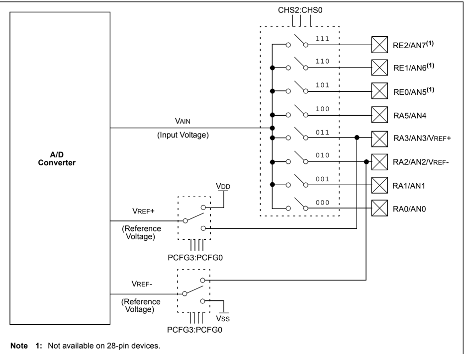
The ADRESH:ADRESL registers contain the 10-bit result of the A/D conversion. When the A/D conversion is complete, the result is loaded into this A/D Result register pair, the GO/DONE bit (ADCON0<2>) is cleared and the A/D interrupt flag bit ADIF is set. The block diagram of the A/D module is shown in Figure 11-1.
After the A/D module has been configured as desired, the selected channel must be acquired before the conversion is started. The analog input channels must have their corresponding TRIS bits selected as inputs.
To determine sample time, see Section 11.1 “A/D Acquisition Requirements”. After this acquisition time has elapsed, the A/D conversion can be started.
To do an A/D Conversion, follow these steps:
- Configure the A/D module:
- Configure analog pins/voltage reference and digital I/O (ADCON1)
- Select A/D input channel (ADCON0)
- Select A/D conversion clock (ADCON0)
- Turn on A/D module (ADCON0)
- Configure A/D interrupt (if desired):
- Clear ADIF bit
- Set ADIE bit
- Set PEIE bit
- Set GIE bit
- Wait the required acquisition time.
- Start conversion:
- Set GO/DONE bit (ADCON0)
- Wait for A/D conversion to complete by either:
- Polling for the GO/DONE bit to be cleared (interrupts disabled); OR
- Waiting for the A/D interrupt
- Read A/D Result register pair (ADRESH:ADRESL), clear bit ADIF if required.
- For the next conversion, go to step 1 or step 2 as required. The A/D conversion time per bit is defined as TAD.
FIGURE 11-1: A/D BLOCK DIAGRAM
Note 1: Not available on 28-pin devices.
11.1 A/D Acquisition Requirements
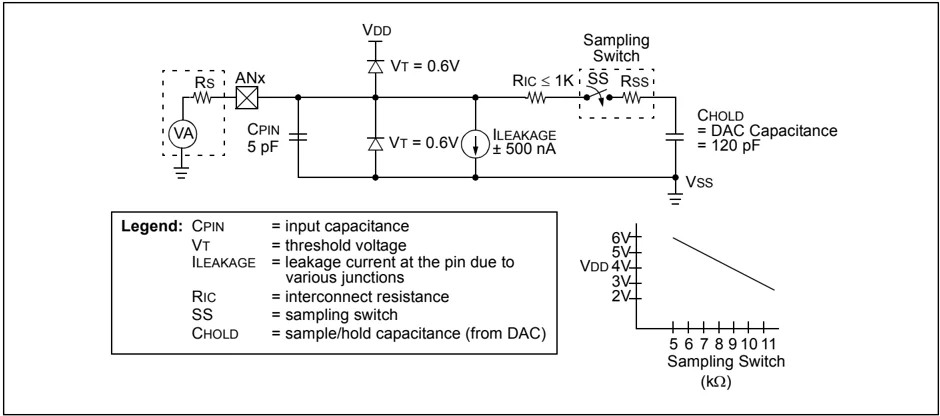
For the A/D converter to meet its specified accuracy, the charge holding capacitor (CHOLD) must be allowed to fully charge to the input channel voltage level. The analog input model is shown in Figure 11-2. The source impedance (Rs) and the internal sampling switch impedance (RSS) directly affect the time required to charge the capacitor CHOLD. The sampling switch (RSS) impedance varies over the device voltage (VDD); see Figure 11-2. The maximum recommended impedance for analog sources is 2.5 kΩ. As the impedance is decreased, the acquisition time may be decreased. After the analog input channel is selected (changed), this acquisition must be done before the conversion can be started.
To calculate the minimum acquisition time, Equation 11-1 may be used. This equation assumes that 1/2 LSb error is used (1024 steps for the A/D). The 1/2 LSb error is the maximum error allowed for the A/D to meet its specified resolution.
To calculate the minimum acquisition time, TACQ, see the PIC® Mid-Range MCU Family Reference Manual (DS33023).
EQUATION 11-1: ACQUISITION TIME
\begin{tabular}{ll} TACQ & = Amplifier Settling Time + Hold Capacitor Charging Time + Temperature Coefficient \ & = TAMP + TC + TCOFF \ TC & = 2 \text{ µs} + TC + [(\text{Temperature} - 25^\circ\text{C})(0.05 \text{ µs}/^\circ\text{C})] \ & = \text{CHOLD (RIC + RSS + Rs) In}(1/2047) \ & = -120 \text{ pF } (1 \text{ k}\Omega + 7 \text{ k}\Omega + 10 \text{ k}\Omega) \text{ In}(0.0004885) \ & = 16.47 \text{ µs} \ \text{TACQ} & = 2 \text{ µs} + 16.47 \text{ µs} + [(50^\circ\text{C} - 25^\circ\text{C})(0.05 \text{ µs}/^\circ\text{C})] \ & = 19.72 \text{ µs} \end{tabular}
Note 1: The reference voltage (VREF) has no effect on the equation since it cancels itself out. 2: The charge holding capacitor (CHOLD) is not discharged after each conversion. 3: The maximum recommended impedance for analog sources is 2.5 kΩ. This is required to meet the pin leakage specification.
FIGURE 11-2: ANALOG INPUT MODEL
11.2 Selecting the A/D Conversion Clock
The A/D conversion time per bit is defined as TAD. The A/D conversion requires a minimum 12 TAD per 10-bit conversion. The source of the A/D conversion clock is software selected. The seven possible options for TAD are:
- 2 TOSC
- 4 TOSC
- 8 TOSC
- 16 TOSC
- 32 TOSC
- 64 TOSC
- Internal A/D module RC oscillator (2-6 µs)
For correct A/D conversions, the A/D conversion clock (TAD) must be selected to ensure a minimum TAD time of 1.6 µs.
Table 11-1 shows the resultant TAD times derived from the device operating frequencies and the A/D clock source selected.
11.3 Configuring Analog Port Pins
The ADCON1 and TRIS registers control the operation of the A/D port pins. The port pins that are desired as analog inputs must have their corresponding TRIS bits set (input). If the TRIS bit is cleared (output), the digital output level (VOH or VOL) will be converted.
The A/D operation is independent of the state of the CHS2:CHS0 bits and the TRIS bits.
Note 1: When reading the port register, any pin configured as an analog input channel will read as cleared (a low level). Pins configured as digital inputs will convert an analog input. Analog levels on a digitally configured input will not affect the conversion accuracy.
2: Analog levels on any pin that is defined as a digital input (including the AN7:AN0 pins) may cause the input buffer to consume current that is out of the device specifications.
TABLE 11-1: TAD vs. MAXIMUM DEVICE OPERATING FREQUENCIES (STANDARD DEVICES (F))
\begin{tabular}{|l|c|l|} \hline \multicolumn{2}{|c|}{AD Clock Source (TAD)} & \multirow{2}{*}{Maximum Device Frequency} \ \cline{1-2} Operation & ADCS2:ADCS1:ADCS0 & \ \hline 2 TOSC & 000 & 1.25 MHz \ \hline 4 TOSC & 100 & 2.5 MHz \ \hline 8 TOSC & 001 & 5 MHz \ \hline 16 TOSC & 101 & 10 MHz \ \hline 32 TOSC & 010 & 20 MHz \ \hline 64 TOSC & 110 & 20 MHz \ \hline RC$^{(1, 2, 3)}$ & x11 & (Note 1) \ \hline \end{tabular}
Note 1: The RC source has a typical TAD time of 4 µs but can vary between 2-6 µs. 2: When the device frequencies are greater than 1 MHz, the RC A/D conversion clock source is only recommended for Sleep operation. 3: For extended voltage devices (LF), please refer to Section 17.0 “Electrical Characteristics”.
11.4 A/D Conversions
Clearing the GO/DONE bit during a conversion will abort the current conversion. The A/D Result register pair will NOT be updated with the partially completed A/D conversion sample. That is, the ADRESH:ADRESL registers will continue to contain the value of the last completed conversion (or the last value written to the ADRESH:ADRESL registers). After the A/D conversion is aborted, the next acquisition on the selected channel is automatically started. The GO/DONE bit can then be set to start the conversion.
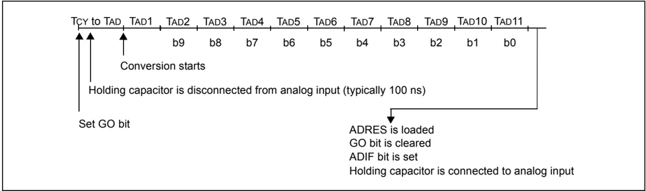
In Figure 11-3, after the GO bit is set, the first time segment has a minimum of T${CY}$ and a maximum of T${AD}$.
Note: The GO/DONE bit should NOT be set in the same instruction that turns on the A/D.
FIGURE 11-3: A/D CONVERSION T$_{AD}$ CYCLES
11.4.1 A/D RESULT REGISTERS
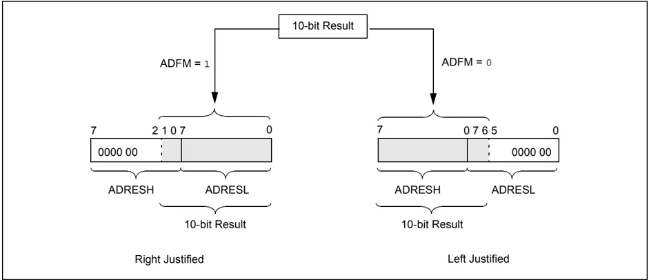
The ADRESH:ADRESL register pair is the location where the 10-bit A/D result is loaded at the completion of the A/D conversion. This register pair is 16 bits wide. The A/D module gives the flexibility to left or right justify the 10-bit result in the 16-bit result register. The A/D Format Select bit (ADFM) controls this justification. Figure 11-4 shows the operation of the A/D result justification. The extra bits are loaded with '0's. When an A/D result will not overwrite these locations (A/D disable), these registers may be used as two general purpose 8-bit registers.
FIGURE 11-4: A/D RESULT JUSTIFICATION
11.5 A/D Operation During Sleep
The A/D module can operate during Sleep mode. This requires that the A/D clock source be set to RC (ADCS1:ADCS0 = 11). When the RC clock source is selected, the A/D module waits one instruction cycle before starting the conversion. This allows the SLEEP instruction to be executed which eliminates all digital switching noise from the conversion. When the conversion is completed, the GO/DONE bit will be cleared and the result loaded into the ADRES register. If the A/D interrupt is enabled, the device will wake-up from Sleep. If the A/D interrupt is not enabled, the A/D module will then be turned off, although the ADON bit will remain set.
When the A/D clock source is another clock option (not RC), a SLEEP instruction will cause the present conversion to be aborted and the A/D module to be turned off, though the ADON bit will remain set.
Turning off the A/D places the A/D module in its lowest current consumption state.
Note: For the A/D module to operate in Sleep, the A/D clock source must be set to RC (ADCS1:ADCS0 = 11). To allow the conversion to occur during Sleep, ensure the SLEEP instruction immediately follows the instruction that sets the GO/DONE bit.
11.6 Effects of a Reset
A device Reset forces all registers to their Reset state. This forces the A/D module to be turned off and any conversion is aborted. All A/D input pins are configured as analog inputs.
The value that is in the ADRESH:ADRESL registers is not modified for a Power-on Reset. The ADRESH:ADRESL registers will contain unknown data after a Power-on Reset.
TABLE 11-2: REGISTERS/BITS ASSOCIATED WITH A/D
| Address | Name | Bit 7 | Bit 6 | Bit 5 | Bit 4 | Bit 3 | Bit 2 | Bit 1 | Bit 0 | Value on POR, BOR | Value on MCLR, WDT |
|---|---|---|---|---|---|---|---|---|---|---|---|
| 0Bh,8Bh,10Bh,18Bh | INTCON | GIE | PEIE | TMR0IE | INTE | RBIE | TMR0IF | INTF | RBIF | 0000 000x | 0000 000u |
| 0Ch | PIR1 | PSPIF⁽¹⁾ | ADIF | RCIF | TXIF | SSPIF | CCP1IF | TMR2IF | TMR1IF | 0000 0000 | 0000 0000 |
| 8Ch | PIE1 | PSPIE⁽¹⁾ | ADIE | RCIE | TXIE | SSPIE | CCP1IE | TMR2IE | TMR1IE | 0000 0000 | 0000 0000 |
| 1Eh | ADRESH | A/D Result Register High Byte | xxxx xxxx | uuuu uuuu | |||||||
| 9Eh | ADRESL | A/D Result Register Low Byte | xxxx xxxx | uuuu uuuu | |||||||
| 1Fh | ADCON0 | ADCS1 | ADCS0 | CHS2 | CHS1 | CHS0 | GO/DONE | — | ADON | 0000 00-0 | 0000 00-0 |
| 9Fh | ADCON1 | ADFM | ADCS2 | — | — | PCFG3 | PCFG2 | PCFG1 | PCFG0 | 00-- 0000 | 00-- 0000 |
| 85h | TRISA | — | — | PORTA Data Direction Register | --11 1111 | --11 1111 | |||||
| 05h | PORTA | — | — | PORTA Data Latch when written: PORTA pins when read | --0x 0000 | --0u 0000 | |||||
| 89h⁽¹⁾ | TRISE | IBF | OBF | IBOV | PSPMODE | — | PORTE Data Direction bits | 0000 -111 | 0000 -111 | ||
| 09h⁽¹⁾ | PORTE | — | — | — | — | — | RE2 | RE1 | RE0 | ---- -xxx | ---- -uuu |
Legend: x = unknown, u = unchanged, - = unimplemented, read as ‘0’. Shaded cells are not used for A/D conversion.
Note 1: These registers are not available on 28-pin devices.
NOTES:
DS39582C-page 134 © 2001-2013 Microchip Technology Inc.
12.0 COMPARATOR MODULE
The comparator module contains two analog comparators. The inputs to the comparators are multiplexed with I/O port pins RA0 through RA3, while the outputs are multiplexed to pins RA4 and RA5. The on-chip voltage reference (Section 13.0 "Comparator Voltage Reference Module") can also be an input to the comparators.
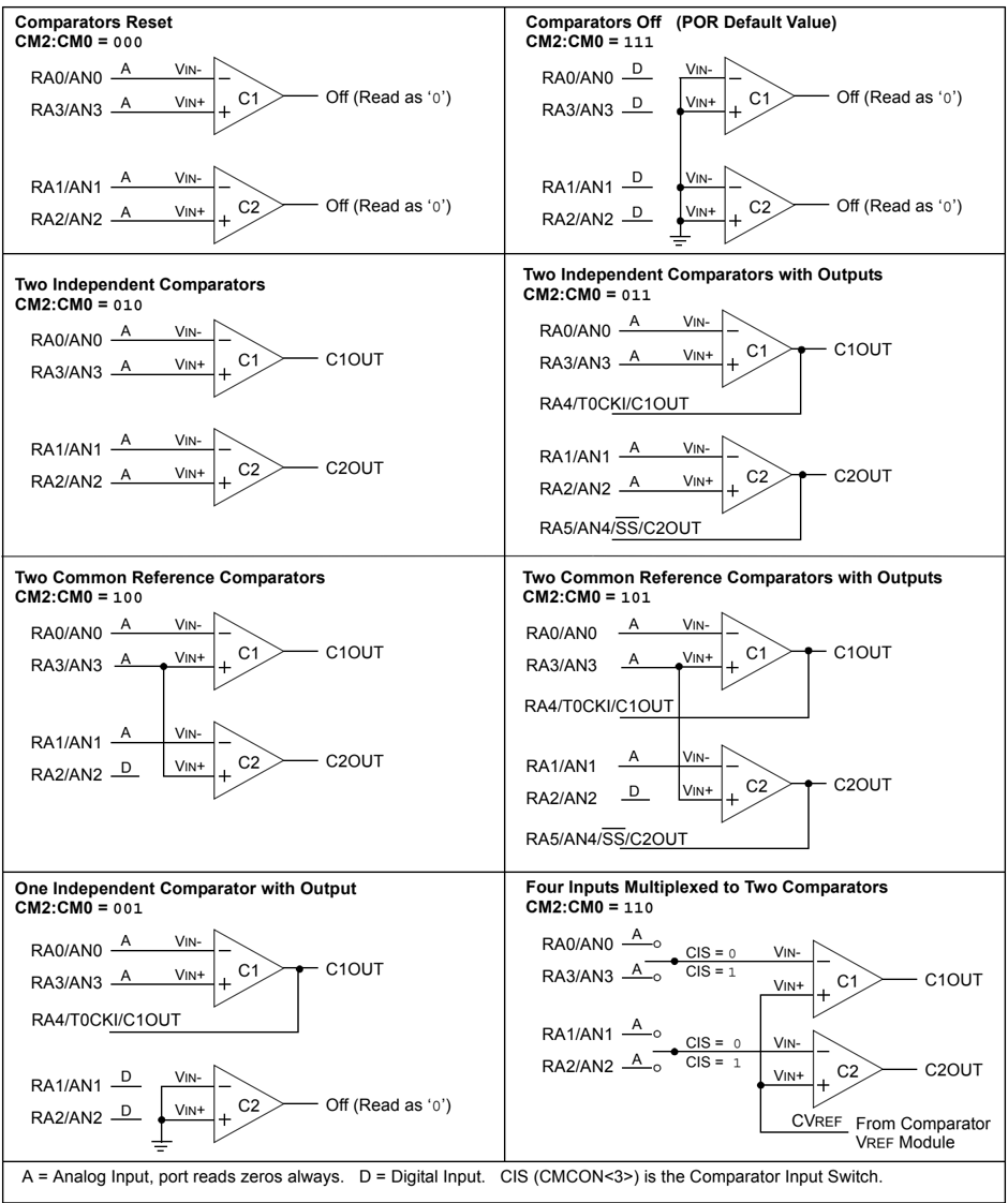
The CMCON register (Register 12-1) controls the comparator input and output multiplexers. A block diagram of the various comparator configurations is shown in Figure 12-1.
REGISTER 12-1: CMCON REGISTER
bit 7 C2OUT: Comparator 2 Output bit When C2INV = 0: 1 = C2 VIN+ > C2 VIN- 0 = C2 VIN+ < C2 VIN- When C2INV = 1: 1 = C2 VIN+ < C2 VIN- 0 = C2 VIN+ > C2 VIN-
bit 6 C1OUT: Comparator 1 Output bit When C1INV = 0: 1 = C1 VIN+ > C1 VIN- 0 = C1 VIN+ < C1 VIN- When C1INV = 1: 1 = C1 VIN+ < C1 VIN- 0 = C1 VIN+ > C1 VIN-
bit 5 C2INV: Comparator 2 Output Inversion bit 1 = C2 output inverted 0 = C2 output not inverted
bit 4 C1INV: Comparator 1 Output Inversion bit 1 = C1 output inverted 0 = C1 output not inverted
bit 3 CIS: Comparator Input Switch bit When CM2:CM0 = 110: 1 = C1 VIN- connects to RA3/AN3 C2 VIN- connects to RA2/AN2 0 = C1 VIN- connects to RA0/AN0 C2 VIN- connects to RA1/AN1
bit 2 CM2:CM0: Comparator Mode bits Figure 12-1 shows the Comparator modes and CM2:CM0 bit settings.
Legend: R = Readable bit W = Writable bit U = Unimplemented bit, read as ‘0’
- n = Value at POR ‘1’ = Bit is set ‘0’ = Bit is cleared x = Bit is unknown
12.1 Comparator Configuration
There are eight modes of operation for the comparators. The CMCON register is used to select these modes. Figure 12-1 shows the eight possible modes. The TRISA register controls the data direction of the comparator pins for each mode. If the Comparator mode is changed, the comparator output level may not be valid for the specified mode change delay shown in Section 17.0 “Electrical Characteristics”.
Note: Comparator interrupts should be disabled during a Comparator mode change. Otherwise, a false interrupt may occur.
FIGURE 12-1: COMPARATOR I/O OPERATING MODES
| Comparators Reset CM2:CM0 = 000 | Comparators Off (POR Default Value) CM2:CM0 = 111 |
|---|---|
| RA0/AN0 A VIN-RA3/AN3 A VIN+Off (Read as ‘0’)RA1/AN1 A VIN-RA2/AN2 A VIN+Off (Read as ‘0’) | RA0/AN0 D VIN-RA3/AN3 D VIN+Off (Read as ‘0’)RA1/AN1 D VIN-RA2/AN2 D VIN+Off (Read as ‘0’) |
| Two Independent Comparators CM2:CM0 = 010 | Two Independent Comparators with Outputs CM2:CM0 = 011 |
|---|---|
| RA0/AN0 A VIN-RA3/AN3 A VIN+C1OUTRA1/AN1 A VIN-RA2/AN2 A VIN+C2OUT | RA0/AN0 A VIN-RA3/AN3 A VIN+C1OUTRA4/T0CKI/C1OUTRA1/AN1 A VIN-RA2/AN2 A VIN+C2OUTRA5/AN4/SS/C2OUT |
| Two Common Reference Comparators CM2:CM0 = 100 | Two Common Reference Comparators with Outputs CM2:CM0 = 101 |
|---|---|
| RA0/AN0 A VIN-RA3/AN3 A VIN+C1OUTRA1/AN1 A VIN-RA2/AN2 D VIN+C2OUT | RA0/AN0 A VIN-RA3/AN3 A VIN+C1OUTRA4/T0CKI/C1OUTRA1/AN1 A VIN-RA2/AN2 D VIN+C2OUTRA5/AN4/SS/C2OUT |
| One Independent Comparator with Output CM2:CM0 = 001 | Four Inputs Multiplexed to Two Comparators CM2:CM0 = 110 |
|---|---|
| RA0/AN0 A VIN-RA3/AN3 A VIN+C1OUTRA4/T0CKI/C1OUTRA1/AN1 D VIN-RA2/AN2 D VIN+Off (Read as ‘0’) | RA0/AN0 A○ CIS = 0 VIN-RA3/AN3 A○ CIS = 1 VIN+C1OUTRA1/AN1 A○ CIS = 0 VIN-RA2/AN2 A○ CIS = 1 VIN+C2OUTCVREF From Comparator VREF Module |
A = Analog Input, port reads zeros always. D = Digital Input. CIS (CMCON<3>) is the Comparator Input Switch.
12.2 Comparator Operation
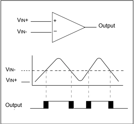
A single comparator is shown in Figure 12-2 along with the relationship between the analog input levels and the digital output. When the analog input at VIN+ is less than the analog input VIN-, the output of the comparator is a digital low level. When the analog input at VIN+ is greater than the analog input VIN-, the output of the comparator is a digital high level. The shaded areas of the output of the comparator in Figure 12-2 represent the uncertainty due to input offsets and response time.
12.3 Comparator Reference
An external or internal reference signal may be used depending on the comparator operating mode. The analog signal present at VIN- is compared to the signal at VIN+ and the digital output of the comparator is adjusted accordingly (Figure 12-2).
FIGURE 12-2: SINGLE COMPARATOR
12.3.1 EXTERNAL REFERENCE SIGNAL
When external voltage references are used, the comparator module can be configured to have the comparators operate from the same or different reference sources. However, threshold detector applications may require the same reference. The reference signal must be between VSS and VDD and can be applied to either pin of the comparator(s).
12.3.2 INTERNAL REFERENCE SIGNAL
The comparator module also allows the selection of an internally generated voltage reference for the comparators. Section 13.0 “Comparator Voltage Reference Module” contains a detailed description of the Comparator Voltage Reference module that provides this signal. The internal reference signal is used when comparators are in mode, CM<2:0> = 110 (Figure 12-1). In this mode, the internal voltage reference is applied to the VIN+ pin of both comparators.
12.4 Comparator Response Time
Response time is the minimum time, after selecting a new reference voltage or input source, before the comparator output has a valid level. If the internal reference is changed, the maximum delay of the internal voltage reference must be considered when using the comparator outputs. Otherwise, the maximum delay of the comparators should be used (Section 17.0 “Electrical Characteristics”).
12.5 Comparator Outputs
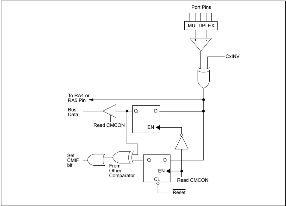
The comparator outputs are read through the CMCON register. These bits are read-only. The comparator outputs may also be directly output to the RA4 and RA5 I/O pins. When enabled, multiplexors in the output path of the RA4 and RA5 pins will switch and the output of each pin will be the unsynchronized output of the comparator. The uncertainty of each of the comparators is related to the input offset voltage and the response time given in the specifications. Figure 12-3 shows the comparator output block diagram.
The TRISA bits will still function as an output enable/disable for the RA4 and RA5 pins while in this mode.
The polarity of the comparator outputs can be changed using the C2INV and C1INV bits (CMCON<4:5>).
Note 1: When reading the Port register, all pins configured as analog inputs will read as a ‘0’. Pins configured as digital inputs will convert an analog input according to the Schmitt Trigger input specification. 2: Analog levels on any pin defined as a digital input may cause the input buffer to consume more current than is specified. 3: RA4 is an open collector I/O pin. When used as an output, a pull-up resistor is required.
FIGURE 12-3: COMPARATOR OUTPUT BLOCK DIAGRAM
12.6 Comparator Interrupts
The comparator interrupt flag is set whenever there is a change in the output value of either comparator. Software will need to maintain information about the status of the output bits, as read from CMCON<7:6>, to determine the actual change that occurred. The CMIF bit (PIR registers) is the Comparator Interrupt Flag. The CMIF bit must be reset by clearing it ('0'). Since it is also possible to write a '1' to this register, a simulated interrupt may be initiated.
The CMIE bit (PIE registers) and the PEIE bit (INTCON register) must be set to enable the interrupt. In addition, the GIE bit must also be set. If any of these bits are clear, the interrupt is not enabled, though the CMIF bit will still be set if an interrupt condition occurs.
Note: If a change in the CMCON register (C1OUT or C2OUT) should occur when a read operation is being executed (start of the Q2 cycle), then the CMIF (PIR registers) interrupt flag may not get set.
The user, in the Interrupt Service Routine, can clear the interrupt in the following manner: a) Any read or write of CMCON will end the mismatch condition. b) Clear flag bit CMIF.
A mismatch condition will continue to set flag bit CMIF. Reading CMCON will end the mismatch condition and allow flag bit CMIF to be cleared.
DS39582C-page 138 © 2001-2013 Microchip Technology Inc.
12.7 Comparator Operation During Sleep
When a comparator is active and the device is placed in Sleep mode, the comparator remains active and the interrupt is functional if enabled. This interrupt will wake-up the device from Sleep mode when enabled. While the comparator is powered up, higher Sleep currents than shown in the power-down current specification will occur. Each operational comparator will consume additional current as shown in the comparator specifications. To minimize power consumption while in Sleep mode, turn off the comparators, CM<2:0> = 111, before entering Sleep. If the device wakes up from Sleep, the contents of the CMCON register are not affected.
12.8 Effects of a Reset
A device Reset forces the CMCON register to its Reset state, causing the comparator module to be in the Comparator Off mode, CM<2:0> = 111. This ensures compatibility to the PIC16F87X devices.
12.9 Analog Input Connection Considerations
A simplified circuit for an analog input is shown in Figure 12-4. Since the analog pins are connected to a digital output, they have reverse biased diodes to VDD and VSS. The analog input, therefore, must be between VSS and VDD. If the input voltage deviates from this range by more than 0.6V in either direction, one of the diodes is forward biased and a latch-up condition may occur. A maximum source impedance of 10 kΩ is recommended for the analog sources. Any external component connected to an analog input pin, such as a capacitor or a Zener diode, should have very little leakage current.
FIGURE 12-4: ANALOG INPUT MODEL
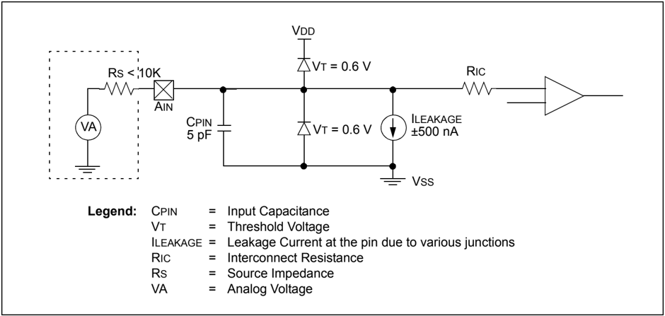
Legend: CPIN = Input Capacitance VT = Threshold Voltage ILEAKAGE = Leakage Current at the pin due to various junctions RIC = Interconnect Resistance Rs = Source Impedance VA = Analog Voltage
TABLE 12-1: REGISTERS ASSOCIATED WITH COMPARATOR MODULE
| Address | Name | Bit 7 | Bit 6 | Bit 5 | Bit 4 | Bit 3 | Bit 2 | Bit 1 | Bit 0 | Value on POR | Value on all other Resets |
|---|---|---|---|---|---|---|---|---|---|---|---|
| 9Ch | CMCON | C2OUT | C1OUT | C2INV | C1INV | CIS | CM2 | CM1 | CM0 | 0000 0111 | 0000 0111 |
| 9Dh | CVRCON | CVREN | CVROE | CVRR | — | CVR3 | CVR2 | CVR1 | CVR0 | 000- 0000 | 000- 0000 |
| 0Bh, 8Bh, 10Bh,18Bh | INTCON | GIE/ GIEH | PEIE/ GIEL | TMR0IE | INTIE | RBIE | TMR0IF | INTIF | RBIF | 0000 000x | 0000 000u |
| 0Dh | PIR2 | — | CMIF | — | — | BCLIF | LVDIF | TMR3IF | CCP2IF | -0-- 0000 | -0-- 0000 |
| 8Dh | PIE2 | — | CMIE | — | — | BCLIE | LVDIE | TMR3IE | CCP2IE | -0-- 0000 | -0-- 0000 |
| 05h | PORTA | — | — | RA5 | RA4 | RA3 | RA2 | RA1 | RA0 | --0x 0000 | --0u 0000 |
| 85h | TRISA | — | — | PORTA Data Direction Register | --11 1111 | --11 1111 |
Legend: x = unknown, u = unchanged, - = unimplemented, read as ‘0’. Shaded cells are unused by the comparator module.
13.0 COMPARATOR VOLTAGE REFERENCE MODULE
The Comparator Voltage Reference Generator is a 16-tap resistor ladder network that provides a fixed voltage reference when the comparators are in mode ‘110’. A programmable register controls the function of the reference generator. Register 13-1 lists the bit functions of the CVRCON register.
As shown in Figure 13-1, the resistor ladder is segmented to provide two ranges of CVREF values and has a power-down function to conserve power when the reference is not being used. The comparator reference supply voltage (also referred to as CVRSRC) comes directly from VDD. It should be noted, however, that the voltage at the top of the ladder is CVRSRC – VSAT, where VSAT is the saturation voltage of the power switch transistor. This reference will only be as accurate as the values of CVRSRC and VSAT.
The output of the reference generator may be connected to the RA2/AN2/VREF-/CVREF pin. This can be used as a simple D/A function by the user if a very high-impedance load is used. The primary purpose of this function is to provide a test path for testing the reference generator function.
REGISTER 13-1: CVRCON CONTROL REGISTER (ADDRESS 9Dh)
bit 7 CVREN: Comparator Voltage Reference Enable bit 1 = CVREF circuit powered on 0 = CVREF circuit powered down
bit 6 CVROE: Comparator VREF Output Enable bit 1 = CVREF voltage level is output on RA2/AN2/VREF-/CVREF pin 0 = CVREF voltage level is disconnected from RA2/AN2/VREF-/CVREF pin
bit 5 CVRR: Comparator VREF Range Selection bit 1 = 0 to 0.75 CVRSRC, with CVRSRC/24 step size 0 = 0.25 CVRSRC to 0.75 CVRSRC, with CVRSRC/32 step size
bit 4 Unimplemented: Read as ‘0’
bit 3-0 CVR3:CVR0: Comparator VREF Value Selection bits 0 \leq VR3:VR0 \leq 15 When CVRR = 1: CVREF = (VR<3:0>/ 24) • (CVRSRC) When CVRR = 0: CVREF = 1/4 • (CVRSRC) + (VR3:VR0/ 32) • (CVRSRC)
Legend: R = Readable bit W = Writable bit U = Unimplemented bit, read as ‘0’ -n = Value at POR ‘1’ = Bit is set ‘0’ = Bit is cleared x = Bit is unknown
FIGURE 13-1: COMPARATOR VOLTAGE REFERENCE BLOCK DIAGRAM
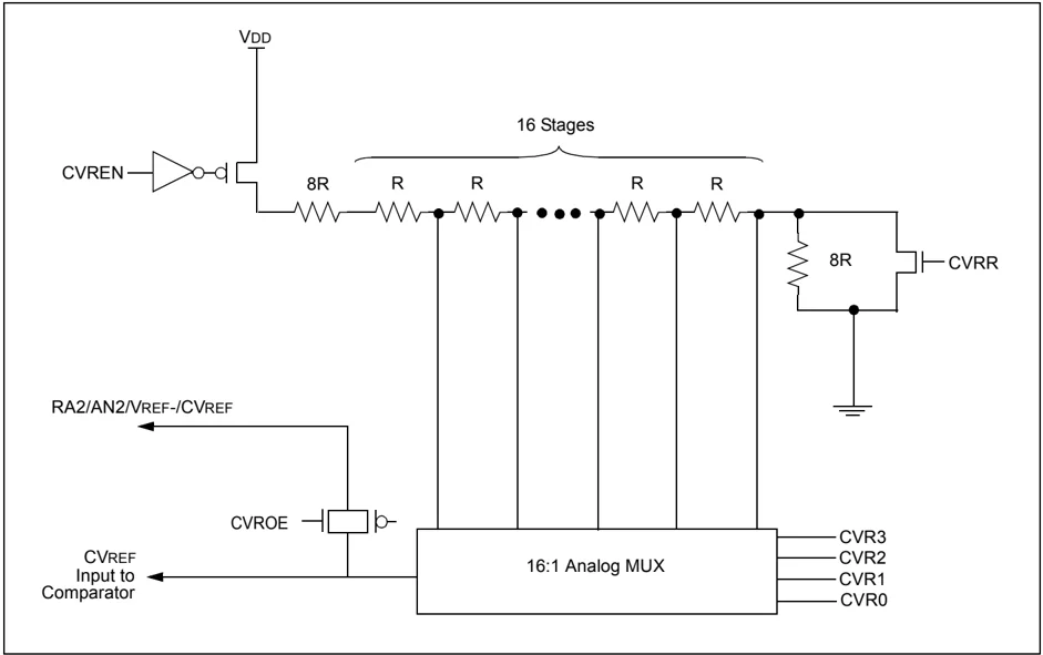
TABLE 13-1: REGISTERS ASSOCIATED WITH COMPARATOR VOLTAGE REFERENCE
| Address | Name | Bit 7 | Bit 6 | Bit 5 | Bit 4 | Bit 3 | Bit 2 | Bit 1 | Bit 0 | Value on POR | Value on all other Resets |
|---|---|---|---|---|---|---|---|---|---|---|---|
| 9Dh | CVRCON | CVREN | CVROE | CVRR | — | CVR3 | CVR2 | CVR1 | CVR0 | 000- 0000 | 000- 0000 |
| 9Ch | CMCON | C2OUT | C1OUT | C2INV | C1INV | CIS | CM2 | CM1 | CM0 | 0000 0111 | 0000 0111 |
Legend: x = unknown, u = unchanged, - = unimplemented, read as ‘0’. Shaded cells are not used with the comparator voltage reference.