7 Parameter Measurement Information
 Figure 7-1. Test Circuit for $V_{KA} = V_{ref}$
 $V_KA = V_ref \left(1 + R1/R2\right) + I_ref × R1$
Figure 7-2. Test Circuit for $V_{KA} > V_{ref}$
 Figure 7-3. Test Circuit for $I_{off}$
7.1 Temperature Coefficient
The deviation of the reference voltage, $V_{ref}$, over the full temperature range is known as $V_{I(dev)}$. The parameter of $V_{I(dev)}$ can be used to find the temperature coefficient of the device. The average full-range temperature coefficient of the reference input voltage, \alpha_Vref, is defined as:
$$\left|\alpha_{vref}\right| \left(\frac{\text{ppm}}{^{\circ}\text{C}}\right) = \frac{\left(\frac{V_{I(dev)}}{V_{ref} \text{ at } 25^{\circ}\text{C}}\right) \times 10^6}{\Delta T_A}$$
where: \Delta T_A is the rated operating temperature range of the device.
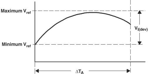
\alpha_Vref is positive or negative, depending on whether minimum $V_{ref}$ or maximum $V_{ref}$, respectively, occurs at the lower temperature. The full-range temperature coefficient is an average and therefore any subsection of the rated operating temperature range can yield a value that is greater or less than the average. For more details on temperature coefficient, refer to the Voltage Reference Selection Basics White Paper.
TL431, TL432
SLVS543S – AUGUST 2004 – REVISED MAY 2024
7.2 Dynamic Impedance
The dynamic impedance is defined as |Z_KA| = \frac\Delta V_KA\Delta I_KA. When the device is operating with two external resistors (see Figure 6-13), the total dynamic impedance of the circuit is given by |z'| = \Delta V/\Delta I, which is approximately equal to |Z_KA|(1 + R1/R2).
The $V_{KA}$ of the device can be affected by the dynamic impedance. The device test current $I_{test}$ for $V_{KA}$ is specified in the Electrical Characteristics. Any deviation from $I_{test}$ can cause deviation on the output $V_{KA}$. Figure 7-4 shows the effect of the dynamic impedance on the $V_{KA}$.
 Figure 7-4. Dynamic Impedance
20 Submit Document Feedback Copyright © 2024 Texas Instruments Incorporated Product Folder Links: TL431 TL432

8 Detailed Description
8.1 Overview
This standard device has proven ubiquity and versatility across a wide range of applications, ranging from power to signal path. This is due to its key components containing an accurate voltage reference & opamp, which are very fundamental analog building blocks. TL43xx is used in conjunction with its key components to behave as a single voltage reference, error amplifier, voltage clamp or comparator with integrated reference.
TL43xx can be operated and adjusted to cathode voltages from 2.5V to 36V, making this part optimum for a wide range of end equipments in industrial, auto, telecom & computing. In order for this device to behave as a shunt regulator or error amplifier, >1mA (Imin(max)) must be supplied in to the cathode pin. Under this condition, feedback can be applied from the Cathode and Ref pins to create a replica of the internal reference voltage.
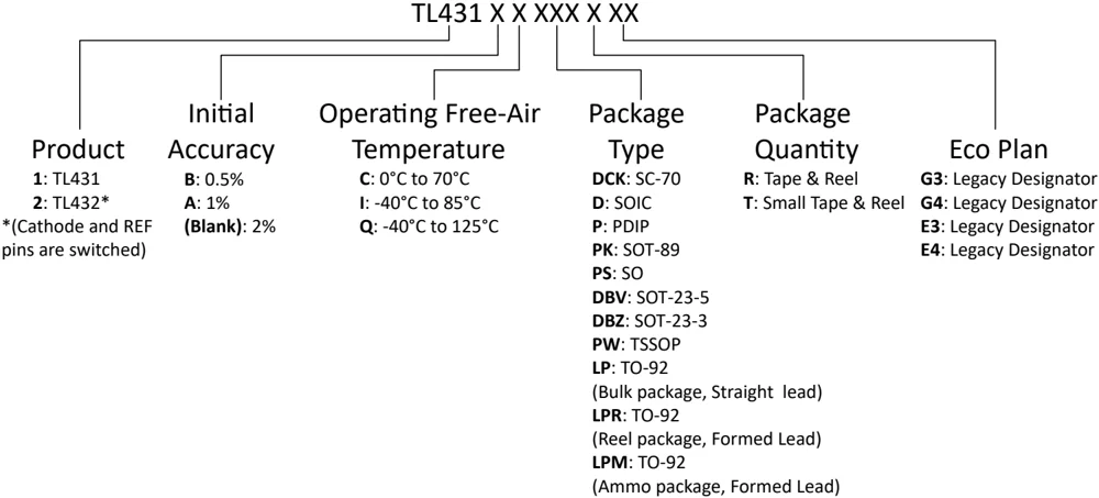
Various reference voltage options can be purchased with initial tolerances (at 25°C) of 0.5%, 1%, and 2%. These reference options are denoted by B (0.5%), A (1.0%) and blank (2.0%) after the TL431 or TL432. TL431 & TL432 are both functionaly, but have separate pinout options.
The TL43xxC devices are characterized for operation from 0°C to 70°C, the TL43xxI devices are characterized for operation from –40°C to 85°C, and the TL43xxQ devices are characterized for operation from –40°C to 125°C.
8.2 Functional Block Diagram
 Figure 8-1. Equivalent Schematic
 Figure 8-2. Detailed Schematic
8.3 Feature Description
TL43xx consists of an internal reference and amplifier that outputs a sink current base on the difference between the reference pin and the virtual internal pin. The sink current is produced by the internal Darlington pair, shown in the above schematic (Figure 8-2). A Darlington pair is used for this device to be able to sink a maximum current of 100mA.
When operated with enough voltage headroom (≥ 2.5V) and cathode current (IKA), TL431 forces the reference pin to 2.5V. However, the reference pin can not be left floating, as it needs IREF ≥ 4μA (please see Electrical Characteristics, TL431C, TL432C). This is because the reference pin is driven into an npn, which needs base current in order operate properly.
When feedback is applied from the Cathode and Reference pins, TL43xx behaves as a Zener diode, regulating to a constant voltage dependent on current being supplied into the cathode. This is due to the internal amplifier and reference entering the proper operating regions. The same amount of current needed in the above feedback situation must be applied to this device in open loop, servo or error amplifying implementations for it to be in the proper linear region giving TL43xx enough gain.
Unlike many linear regulators, TL43xx is internally compensated to be stable without an output capacitor between the cathode and anode. However, if it is desired to use an output capacitor Figure 6-18 can be used as a guide to assist in choosing the correct capacitor to maintain stability.
8.4 Device Functional Modes
8.4.1 Open Loop (Comparator)
When the cathode/output voltage or current of TL43xx is not being fed back to the reference/input pin in any form, this device is operating in open loop. With proper cathode current (Ika) applied to this device, TL43xx will have the characteristics shown in Figure 9-2. With such high gain in this configuration, TL43xx is typically used as a comparator. With the reference integrated makes TL43xx the preferred choice when users are trying to monitor a certain level of a single signal.
8.4.2 Closed Loop
When the cathode/output voltage or current of TL43xx is being fed back to the reference/input pin in any form, this device is operating in closed loop. The majority of applications involving TL43xx use it in this manner to regulate a fixed voltage or current. The feedback enables this device to behave as an error amplifier, computing a portion of the output voltage and adjusting it to maintain the desired regulation. This is done by relating the output voltage back to the reference pin in a manner to make it equal to the internal reference voltage, which can be accomplished via resistive or direct feedback.

9 Applications and Implementation
Note
Information in the following applications sections is not part of the TI component specification, and TI does not warrant its accuracy or completeness. TI's customers are responsible for determining suitability of components for their purposes. Customers should validate and test their design implementation to confirm system functionality.
9.1 Application Information
As this device has many applications and setups, there are many situations that this datasheet can not characterize in detail. The linked application notes will help the designer make the best choices when using this part.
Application note Understanding Stability Boundary Conditions Charts in TL431, TL432 Data Sheet (SLVA482) will provide a deeper understanding of this devices stability characteristics and aid the user in making the right choices when choosing a load capacitor. Application note Setting the Shunt Voltage on an Adjustable Shunt Regulator (SLVA445) assists designers in setting the shunt voltage to achieve optimum accuracy for this device.
9.2 Typical Applications
9.2.1 Comparator With Integrated Reference
 Figure 9-1. Comparator Application Schematic
Copyright © 2024 Texas Instruments Incorporated Submit Document Feedback 23 Product Folder Links: TL431 TL432
TL431, TL432
SLVS543S – AUGUST 2004 – REVISED MAY 2024
9.2.1.1 Design Requirements
For this design example, use the parameters listed in Table 9-1 as the input parameters.
Table 9-1. Design Parameters
9.2.1.2 Detailed Design Procedure
When using TL431 as a comparator with reference, determine the following:
• Input Voltage Range
• Reference Voltage Accuracy
• Output logic input high and low level thresholds
• Current Source resistance
9.2.1.2.1 Basic Operation
In the configuration shown in Figure 9-1 TL431 will behave as a comparator, comparing the VREF pin voltage to the internal virtual reference voltage. When provided a proper cathode current (IK), TL43xx will have enough open loop gain to provide a quick response. This can be seen in Figure 9-2, where the RSUP=10 kΩ (IKA=500 μA) situation responds much slower than RSUP=1 kΩ (IKA=5mA). Operation near and below Imin could result in low gain, leading to a slow response.
9.2.1.2.1.1 Overdrive
Slow or inaccurate responses can also occur when the reference pin is not provided enough overdrive voltage. This is the amount of voltage that is higher than the internal virtual reference. The internal virtual reference voltage will be within the range of 2.5V±(0.5%, 1.0% or 1.5%) depending on which version is being used. The more overdrive voltage provided, the faster the TL431 will respond.
For applications where TL431 is being used as a comparator, it is best to set the trip point to greater than the positive expected error (i.e. +1.0% for the A version). For fast response, setting the trip point to >10% of the internal VREF should suffice.
For minimal voltage drop or difference from Vin to the ref pin, it is recommended to use an input resistor <10kΩ to provide Iref.

TL431, TL432
SLVS543S – AUGUST 2004 – REVISED MAY 2024
9.2.1.2.2 Output Voltage and Logic Input Level
For TL431 to properly be used as a comparator, the logic output must be readable by the receiving logic device. This is accomplished by knowing the input high and low level threshold voltage levels, typically denoted by $V_{IH}$ & $V_{IL}$.
As seen in Figure 9-2, TL431's output low level voltage in open-loop/comparator mode is ~2 V, which is typically sufficient for 5V supplied logic. However, would not work for 3.3V& 1.8Vsupplied logic. To accommodate this a resistive divider can be tied to the output to attenuate the output voltage to a voltage legible to the receiving low voltage logic device.
TL431's output high voltage is equal to $V_{SUP}$ due to TL431 being open-collector. If $V_{SUP}$ is much higher than the receiving logic's maximum input voltage tolerance, the output must be attenuated to accommodate the outgoing logic's reliability.
When using a resistive divider on the output, be sure to make the sum of the resistive divider (R1 & R2 in Figure 9-1) is much greater than $R_{SUP}$ to not interfere with TL431's ability to pull close to $V_{SUP}$ when turning off.
9.2.1.2.2.1 Input Resistance
TL431 requires an input resistance in this application to source the reference current ($I_{REF}$) needed from this device to be in the proper operating regions while turning on. The actual voltage seen at the ref pin will be $V_{REF}=V_{IN}-I_{REF}*R_{IN}$. Since $I_{REF}$ can be as high as 4µA it is recommended to use a resistance small enough that will mitigate the error that $I_{REF}$ creates from $V_{IN}$.
9.2.1.3 Application Curve
 Figure 9-2. Output Response With Various Cathode Currents
Copyright © 2024 Texas Instruments Incorporated Submit Document Feedback 25 Product Folder Links: TL431 TL432

TL431, TL432
SLVS543S – AUGUST 2004 – REVISED MAY 2024
9.2.2 Shunt Regulator/Reference
 Figure 9-3. Shunt Regulator Schematic
9.2.2.1 Design Requirements
For this design example, use the parameters listed in Table 9-1 as the input parameters.
Table 9-2. Design Parameters
9.2.2.2 Detailed Design Procedure
When using TL431 as a Shunt Regulator, determine the following:
• Input Voltage Range
• Temperature Range
• Total Accuracy
• Cathode Current
• Reference Initial Accuracy
• Output Capacitance
9.2.2.2.1 Programming Output/Cathode Voltage
In order to program the cathode voltage to a regulated voltage a resistive bridge must be shunted between the cathode and anode pins with the mid point tied to the reference pin. This can be seen in Figure 9-3, with R1 & R2 being the resistive bridge. The cathode/output voltage in the shunt regulator configuration can be approximated by the equation shown in Figure 9-3. The cathode voltage can be more accuratel determined by taking in to account the cathode current:
$$Vo=(1+R1/R2)*V_{REF}-I_{REF}*R1$$
In order for this equation to be valid, TL43xx must be fully biased so that it has enough open loop gain to mitigate any gain error. This can be done by meeting the Imin spec denoted in Electrical Characteristics, TL431C, TL432C.
9.2.2.2.2 Total Accuracy
When programming the output above unity gain (VKA=VREF), TL43xx is susceptible to other errors that may effect the overall accuracy beyond VREF. These errors include:
- R1 and R2 accuracies
- VI(dev) - Change in reference voltage over temperature
- ΔVREF / ΔVKA - Change in reference voltage to the change in cathode voltage
- |zKA| - Dynamic impedance, causing a change in cathode voltage with cathode current
Worst case cathode voltage can be determined taking all of the variables in to account. Application note Setting the Shunt Voltage on an Adjustable Shunt Regulator (SLVA445) assists designers in setting the shunt voltage to achieve optimum accuracy for this device.
9.2.2.2.3 Stability
Though TL43xx is stable with no capacitive load, the device that receives the shunt regulator's output voltage could present a capacitive load that is within the TL43xx region of stability, shown in Figure 6-16 and Figure 6-18. Also, designers may use capacitive loads to improve the transient response or for power supply decoupling. When using additional capacitance between Cathode and Anode, refer to Figure 6-16 and Figure 6-18. Also, application note Understanding Stability Boundary Conditions Charts in TL431, TL432 Data Sheet (SLVA482) will provide a deeper understanding of this devices stability characteristics and aid the user in making the right choices when choosing a load capacitor.
9.2.2.2.4 Start-Up Time
As shown in Figure 9-4, TL43xx has a fast response up to ~2V and then slowly charges to its programmed value. This is due to the compensation capacitance (shown in Figure 6-18) the TL43xx has to meet its stability criteria. Despite the secondary delay, TL43xx still has a fast response suitable for many clamp applications.
9.2.2.3 Application Curve
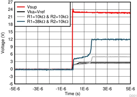
Figure 9-4. TL43xx Start-Up Response

TL431, TL432
SLVS543S – AUGUST 2004 – REVISED MAY 2024
9.3 System Examples
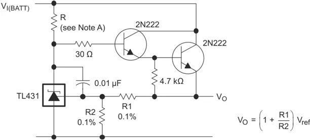
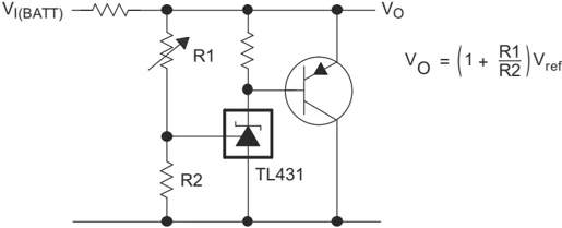
A. R should provide cathode current ≥1mA to the TL431 at minimum $V_{I(BATT)}$.
Figure 9-5. Precision High-Current Series Regulator
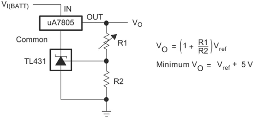
$V_O = \left(1 + R1/R2\right)V_ref$
Minimum $V_O$ = $V_{ref}$ + 5 V
Figure 9-6. Output Control of a Three-Terminal Fixed Regulator
$V_O = \left(1 + R1/R2\right)V_ref$
Figure 9-7. High-Current Shunt Regulator
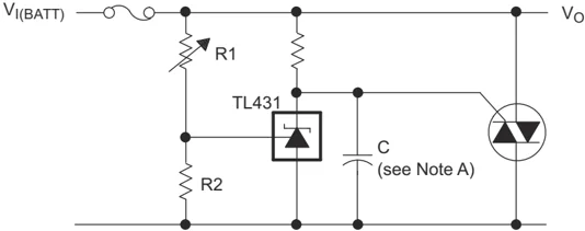
A. Refer to the stability boundary conditions in Figure 6-16 and Figure 6-18 to determine allowable values for C.
Figure 9-8. Crowbar Circuit
TEXAS INSTRUMENTS
TL431, TL432 SLVS543S – AUGUST 2004 – REVISED MAY 2024
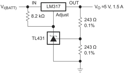
Figure 9-9. Precision 5V, 1.5A Regulator
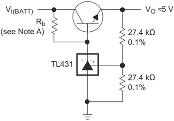
A. Rb should provide cathode current ≥1mA to the TL431.
Figure 9-10. Efficient 5V Precision Regulator

Figure 9-11. PWM Converter With Reference
Copyright © 2024 Texas Instruments Incorporated Submit Document Feedback 29 Product Folder Links: TL431 TL432
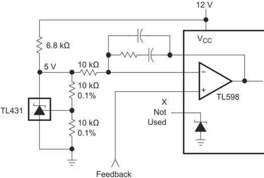
TL431, TL432 SLVS543S – AUGUST 2004 – REVISED MAY 2024
TEXAS INSTRUMENTS www.ti.com
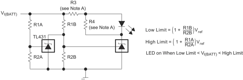
A. Select R3 and R4 to provide the desired LED intensity and cathode current ≥1mA to the TL431 at the available $V_{I(BATT)}$.
Figure 9-12. Voltage Monitor
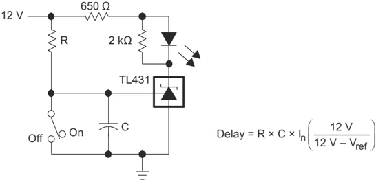
Figure 9-13. Delay Timer
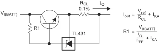
Figure 9-14. Precision Current Limiter
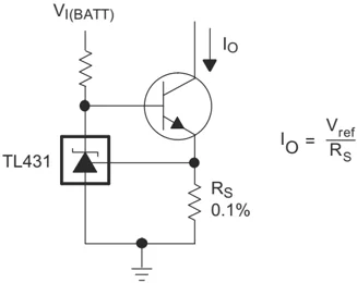
Figure 9-15. Precision Constant-Current Sink
30 Submit Document Feedback Copyright © 2024 Texas Instruments Incorporated Product Folder Links: TL431 TL432
9.4 Power Supply Recommendations
When using TL43xx as a Linear Regulator to supply a load, designers will typically use a bypass capacitor on the output/cathode pin. When doing this, be sure that the capacitance is within the stability criteria shown in Figure 6-16 and Figure 6-18.
In order to not exceed the maximum cathode current, be sure that the supply voltage is current limited. Also, be sure to limit the current being driven into the Ref pin, as not to exceed its absolute maximum rating.
For applications shunting high currents, pay attention to the cathode and anode trace lengths, adjusting the width of the traces to have the proper current density.
9.5 Layout
9.5.1 Layout Guidelines
Bypass capacitors should be placed as close to the part as possible. Current-carrying traces need to have widths appropriate for the amount of current they are carrying; in the case of the TL43xx, these currents will be low.
9.5.2 Layout Example
 Figure 9-16. DBZ Layout Example
Copyright © 2024 Texas Instruments Incorporated Submit Document Feedback 31 Product Folder Links: TL431 TL432

10 Device and Documentation Support
10.1 Device Nomenclature
TI assigns suffixes and prefixes to differentiate all the combinations of the TL43x family. The Eco Plan designator is a legacy designator that was used to differentiate Pb-free and Green devices. More details and possible orderable combinations are located on the Package Option Addendum in Mechanical, Packaging, and Orderable Information.
10.2 Related Links
The table below lists quick access links. Categories include technical documents, support and community resources, tools and software, and quick access to sample or buy.
Table 10-1. Related Links
| PARTS | PRODUCT FOLDER | SAMPLE & BUY | TECHNICAL DOCUMENTS | TOOLS & SOFTWARE | SUPPORT & COMMUNITY |
|---|---|---|---|---|---|
| TL431 | Click here | Click here | Click here | Click here | Click here |
| TL432 | Click here | Click here | Click here | Click here | Click here |
10.3 Receiving Notification of Documentation Updates
To receive notification of documentation updates, navigate to the device product folder on ti.com. Click on Notifications to register and receive a weekly digest of any product information that has changed. For change details, review the revision history included in any revised document.
10.4 Support Resources
TI E2E™ support forums are an engineer's go-to source for fast, verified answers and design help — straight from the experts. Search existing answers or ask your own question to get the quick design help you need.
Linked content is provided "AS IS" by the respective contributors. They do not constitute TI specifications and do not necessarily reflect TI's views; see TI's Terms of Use.
10.5 Trademarks
TI E2E™ is a trademark of Texas Instruments.
All trademarks are the property of their respective owners.

10.6 Electrostatic Discharge Caution
 This integrated circuit can be damaged by ESD. Texas Instruments recommends that all integrated circuits be handled with appropriate precautions. Failure to observe proper handling and installation procedures can cause damage.
ESD damage can range from subtle performance degradation to complete device failure. Precision integrated circuits may be more susceptible to damage because very small parametric changes could cause the device not to meet its published specifications.
10.7 Glossary
TI Glossary This glossary lists and explains terms, acronyms, and definitions.
11 Revision History
Changes from Revision R (August 2023) to Revision S (May 2024) Page
- Updated pinout diagrams ........ 4
Changes from Revision Q (July 2022) to Revision R (August 2023) Page
- Updated Applications section links ........ 1
- Updated Description section ........ 1
- Removed KTP package ........ 4
- Added detailed Temperature Coefficient and Dynamic Impedance sections ........ 19
- Updated Applications section ........ 26
- Updated LP package in Device Nomenclature figure ........ 32
Changes from Revision P (November 2018) to Revision Q (July 2022) Page
- Updated the numbering format for tables, figures, and cross-references throughout the document ........ 1
- Corrected the device names in the Pin Functions table ........ 4
Changes from Revision O (January 2015) to Revision P (November 2018) Page
- Added text to the Description section ........ 1
- Added TL43x Device Comparison Table ........ 3
- Added TL43x Device Nomenclature section ........ 32
Changes from Revision N (January 2014) to Revision O (January 2015) Page
- Added Applications, Device Information table, Pin Functions table, ESD Ratings table, Thermal Information table, Feature Description section, Device Functional Modes, Application and Implementation section, Power Supply Recommendations section, Layout section, Device and Documentation Support section, and Mechanical, Packaging, and Orderable Information section ........ 1
- Added Applications ........ 1
12 Mechanical, Packaging, and Orderable Information
The following pages include mechanical packaging and orderable information. This information is the most current data available for the designated devices. This data is subject to change without notice and revision of this document. For browser based versions of this data sheet, refer to the left hand navigation.