PACKAGE MATERIALS INFORMATION
10-Aug-2026
TAPE AND REEL INFORMATION
REEL DIMENSIONS
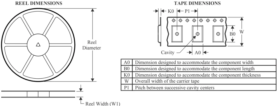
TAPE DIMENSIONS
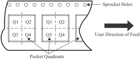
| A0 | Dimension designed to accommodate the component width |
|---|---|
| B0 | Dimension designed to accommodate the component length |
| K0 | Dimension designed to accommodate the component thickness |
| W | Overall width of the carrier tape |
| P1 | Pitch between successive cavity centers |
QUADRANT ASSIGNMENTS FOR PIN 1 ORIENTATION IN TAPE
*All dimensions are nominal
| Device | Package Type | Package Drawing | Pins | SPQ | Reel Diameter (mm) | Reel Width W1 (mm) | A0 (mm) | B0 (mm) | K0 (mm) | P1 (mm) | W (mm) | Pin1 Quadrant |
|---|---|---|---|---|---|---|---|---|---|---|---|---|
| TL431ACDBVR | SOT-23 | DBV | 5 | 3000 | 180.0 | 8.4 | 3.2 | 3.2 | 1.4 | 4.0 | 8.0 | Q3 |
| TL431ACDBVT | SOT-23 | DBV | 5 | 250 | 180.0 | 8.4 | 3.2 | 3.2 | 1.4 | 4.0 | 8.0 | Q3 |
| TL431ACDBVT | SOT-23 | DBV | 5 | 250 | 180.0 | 8.4 | 3.2 | 3.2 | 1.4 | 4.0 | 8.0 | Q3 |
| TL431ACDBZR | SOT-23 | DBZ | 3 | 3000 | 180.0 | 8.4 | 2.9 | 3.35 | 1.35 | 4.0 | 8.0 | Q3 |
| TL431ACDBZRG4 | SOT-23 | DBZ | 3 | 3000 | 180.0 | 8.4 | 2.9 | 3.35 | 1.35 | 4.0 | 8.0 | Q3 |
| TL431ACDBZT | SOT-23 | DBZ | 3 | 250 | 180.0 | 8.4 | 2.9 | 3.35 | 1.35 | 4.0 | 8.0 | Q3 |
| TL431ACDBZT | SOT-23 | DBZ | 3 | 250 | 180.0 | 8.4 | 3.2 | 2.85 | 1.3 | 4.0 | 8.0 | Q3 |
| TL431ACDBZTG4 | SOT-23 | DBZ | 3 | 250 | 180.0 | 8.4 | 2.9 | 3.35 | 1.35 | 4.0 | 8.0 | Q3 |
| TL431ACDCKR | SC70 | DCK | 6 | 3000 | 180.0 | 8.4 | 2.41 | 2.41 | 1.2 | 4.0 | 8.0 | Q3 |
| TL431ACDCKR | SC70 | DCK | 6 | 3000 | 180.0 | 8.4 | 2.3 | 2.55 | 1.2 | 4.0 | 8.0 | Q3 |
| TL431ACDR | SOIC | D | 8 | 2500 | 330.0 | 12.4 | 6.4 | 5.2 | 2.1 | 8.0 | 12.0 | Q1 |
| TL431ACPK | SOT-89 | PK | 3 | 1000 | 180.0 | 12.4 | 4.91 | 4.52 | 1.9 | 8.0 | 12.0 | Q3 |
| TL431ACPK | SOT-89 | PK | 3 | 1000 | 180.0 | 12.4 | 4.91 | 4.52 | 1.9 | 8.0 | 12.0 | Q3 |
| TL431ACPSR | SO | PS | 8 | 2000 | 330.0 | 16.4 | 8.35 | 6.6 | 2.4 | 12.0 | 16.0 | Q1 |
| TL431ACPWR | TSSOP | PW | 8 | 2000 | 330.0 | 12.4 | 7.0 | 3.6 | 1.6 | 8.0 | 12.0 | Q1 |
| TL431AIDBVR | SOT-23 | DBV | 5 | 3000 | 180.0 | 8.4 | 3.2 | 3.2 | 1.4 | 4.0 | 8.0 | Q3 |
Pack Materials-Page 1
PACKAGE MATERIALS INFORMATION
10-Aug-2026
| Device | Package Type | Package Drawing | Pins | SPQ | Reel Diameter (mm) | Reel Width W1 (mm) | A0 (mm) | B0 (mm) | K0 (mm) | P1 (mm) | W (mm) | Pin1 Quadrant |
|---|---|---|---|---|---|---|---|---|---|---|---|---|
| TL431AIDBVT | SOT-23 | DBV | 5 | 250 | 180.0 | 8.4 | 3.2 | 3.2 | 1.4 | 4.0 | 8.0 | Q3 |
| TL431AIDBVT | SOT-23 | DBV | 5 | 250 | 180.0 | 8.4 | 3.2 | 3.2 | 1.4 | 4.0 | 8.0 | Q3 |
| TL431AIDBZR | SOT-23 | DBZ | 3 | 3000 | 180.0 | 8.4 | 2.9 | 3.35 | 1.35 | 4.0 | 8.0 | Q3 |
| TL431AIDBZRG4 | SOT-23 | DBZ | 3 | 3000 | 180.0 | 8.4 | 2.9 | 3.35 | 1.35 | 4.0 | 8.0 | Q3 |
| TL431AIDBZT | SOT-23 | DBZ | 3 | 250 | 180.0 | 8.4 | 3.2 | 2.85 | 1.3 | 4.0 | 8.0 | Q3 |
| TL431AIDBZT | SOT-23 | DBZ | 3 | 250 | 180.0 | 8.4 | 2.9 | 3.35 | 1.35 | 4.0 | 8.0 | Q3 |
| TL431AIDBZTG4 | SOT-23 | DBZ | 3 | 250 | 180.0 | 8.4 | 2.9 | 3.35 | 1.35 | 4.0 | 8.0 | Q3 |
| TL431AIDCKR | SC70 | DCK | 6 | 3000 | 180.0 | 8.4 | 2.3 | 2.55 | 1.2 | 4.0 | 8.0 | Q3 |
| TL431AIDCKR | SC70 | DCK | 6 | 3000 | 179.0 | 8.4 | 2.2 | 2.5 | 1.2 | 4.0 | 8.0 | Q3 |
| TL431AIDCKRG4 | SC70 | DCK | 6 | 3000 | 179.0 | 8.4 | 2.2 | 2.5 | 1.2 | 4.0 | 8.0 | Q3 |
| TL431AIDCKT | SC70 | DCK | 6 | 250 | 179.0 | 8.4 | 2.2 | 2.5 | 1.2 | 4.0 | 8.0 | Q3 |
| TL431AIDCKT | SC70 | DCK | 6 | 250 | 180.0 | 8.4 | 2.3 | 2.55 | 1.2 | 4.0 | 8.0 | Q3 |
| TL431AIDR | SOIC | D | 8 | 2500 | 330.0 | 12.4 | 6.4 | 5.2 | 2.1 | 8.0 | 12.0 | Q1 |
| TL431AIPK | SOT-89 | PK | 3 | 1000 | 180.0 | 12.4 | 4.91 | 4.52 | 1.9 | 8.0 | 12.0 | Q3 |
| TL431AIPK | SOT-89 | PK | 3 | 1000 | 180.0 | 12.4 | 4.91 | 4.52 | 1.9 | 8.0 | 12.0 | Q3 |
| TL431AQDBVR | SOT-23 | DBV | 5 | 3000 | 180.0 | 8.4 | 3.2 | 3.2 | 1.4 | 4.0 | 8.0 | Q3 |
| TL431AQDBVT | SOT-23 | DBV | 5 | 250 | 180.0 | 8.4 | 3.2 | 3.2 | 1.4 | 4.0 | 8.0 | Q3 |
| TL431AQDBZR | SOT-23 | DBZ | 3 | 3000 | 180.0 | 8.4 | 2.9 | 3.35 | 1.35 | 4.0 | 8.0 | Q3 |
| TL431AQDBZRG4 | SOT-23 | DBZ | 3 | 3000 | 180.0 | 8.4 | 2.9 | 3.35 | 1.35 | 4.0 | 8.0 | Q3 |
| TL431AQDBZT | SOT-23 | DBZ | 3 | 250 | 180.0 | 8.4 | 2.9 | 3.35 | 1.35 | 4.0 | 8.0 | Q3 |
| TL431AQDBZT | SOT-23 | DBZ | 3 | 250 | 180.0 | 8.4 | 3.2 | 2.85 | 1.3 | 4.0 | 8.0 | Q3 |
| TL431AQDBZTG4 | SOT-23 | DBZ | 3 | 250 | 180.0 | 8.4 | 2.9 | 3.35 | 1.35 | 4.0 | 8.0 | Q3 |
| TL431AQDCKR | SC70 | DCK | 6 | 3000 | 179.0 | 8.4 | 2.2 | 2.5 | 1.2 | 4.0 | 8.0 | Q3 |
| TL431AQDCKR | SC70 | DCK | 6 | 3000 | 180.0 | 8.4 | 2.3 | 2.55 | 1.2 | 4.0 | 8.0 | Q3 |
| TL431AQDCKT | SC70 | DCK | 6 | 250 | 179.0 | 8.4 | 2.2 | 2.5 | 1.2 | 4.0 | 8.0 | Q3 |
| TL431AQDCKT | SC70 | DCK | 6 | 250 | 180.0 | 8.4 | 2.3 | 2.55 | 1.2 | 4.0 | 8.0 | Q3 |
| TL431AQPK | SOT-89 | PK | 3 | 1000 | 180.0 | 12.4 | 4.91 | 4.52 | 1.9 | 8.0 | 12.0 | Q3 |
| TL431AQPK | SOT-89 | PK | 3 | 1000 | 180.0 | 12.4 | 4.91 | 4.52 | 1.9 | 8.0 | 12.0 | Q3 |
| TL431BCDBVR | SOT-23 | DBV | 5 | 3000 | 180.0 | 8.4 | 3.2 | 3.2 | 1.4 | 4.0 | 8.0 | Q3 |
| TL431BCDBVT | SOT-23 | DBV | 5 | 250 | 180.0 | 8.4 | 3.2 | 3.2 | 1.4 | 4.0 | 8.0 | Q3 |
| TL431BCDBVT | SOT-23 | DBV | 5 | 250 | 180.0 | 8.4 | 3.2 | 3.2 | 1.4 | 4.0 | 8.0 | Q3 |
| TL431BCDBZR | SOT-23 | DBZ | 3 | 3000 | 180.0 | 8.4 | 2.9 | 3.35 | 1.35 | 4.0 | 8.0 | Q3 |
| TL431BCDBZRG4 | SOT-23 | DBZ | 3 | 3000 | 180.0 | 8.4 | 2.9 | 3.35 | 1.35 | 4.0 | 8.0 | Q3 |
| TL431BCDBZT | SOT-23 | DBZ | 3 | 250 | 180.0 | 8.4 | 2.9 | 3.35 | 1.35 | 4.0 | 8.0 | Q3 |
| TL431BCDBZT | SOT-23 | DBZ | 3 | 250 | 180.0 | 8.4 | 3.2 | 2.85 | 1.3 | 4.0 | 8.0 | Q3 |
| TL431BCDBZTG4 | SOT-23 | DBZ | 3 | 250 | 180.0 | 8.4 | 2.9 | 3.35 | 1.35 | 4.0 | 8.0 | Q3 |
| TL431BCDCKR | SC70 | DCK | 6 | 3000 | 179.0 | 8.4 | 2.2 | 2.5 | 1.2 | 4.0 | 8.0 | Q3 |
| TL431BCDCKR | SC70 | DCK | 6 | 3000 | 180.0 | 8.4 | 2.3 | 2.55 | 1.2 | 4.0 | 8.0 | Q3 |
| TL431BCDCKT | SC70 | DCK | 6 | 250 | 180.0 | 8.4 | 2.3 | 2.55 | 1.2 | 4.0 | 8.0 | Q3 |
| TL431BCDCKT | SC70 | DCK | 6 | 250 | 179.0 | 8.4 | 2.2 | 2.5 | 1.2 | 4.0 | 8.0 | Q3 |
| TL431BCDR | SOIC | D | 8 | 2500 | 330.0 | 12.4 | 6.4 | 5.2 | 2.1 | 8.0 | 12.0 | Q1 |
Pack Materials-Page 2
PACKAGE MATERIALS INFORMATION
10-Aug-2026
| Device | Package Type | Package Drawing | Pins | SPQ | Reel Diameter (mm) | Reel Width W1 (mm) | A0 (mm) | B0 (mm) | K0 (mm) | P1 (mm) | W (mm) | Pin1 Quadrant |
|---|---|---|---|---|---|---|---|---|---|---|---|---|
| TL431BCDR | SOIC | D | 8 | 2500 | 330.0 | 12.4 | 6.4 | 5.2 | 2.1 | 8.0 | 12.0 | Q1 |
| TL431BCPK | SOT-89 | PK | 3 | 1000 | 180.0 | 12.4 | 4.91 | 4.52 | 1.9 | 8.0 | 12.0 | Q3 |
| TL431BCPK | SOT-89 | PK | 3 | 1000 | 180.0 | 12.4 | 4.91 | 4.52 | 1.9 | 8.0 | 12.0 | Q3 |
| TL431BIDBVR | SOT-23 | DBV | 5 | 3000 | 178.0 | 8.4 | 3.2 | 3.2 | 1.4 | 4.0 | 8.0 | Q3 |
| TL431BIDBVR | SOT-23 | DBV | 5 | 3000 | 180.0 | 8.4 | 3.2 | 3.2 | 1.4 | 4.0 | 8.0 | Q3 |
| TL431BIDBVT | SOT-23 | DBV | 5 | 250 | 180.0 | 8.4 | 3.2 | 3.2 | 1.4 | 4.0 | 8.0 | Q3 |
| TL431BIDBZR | SOT-23 | DBZ | 3 | 3000 | 180.0 | 8.4 | 2.9 | 3.35 | 1.35 | 4.0 | 8.0 | Q3 |
| TL431BIDBZRG4 | SOT-23 | DBZ | 3 | 3000 | 180.0 | 8.4 | 2.9 | 3.35 | 1.35 | 4.0 | 8.0 | Q3 |
| TL431BIDBZT | SOT-23 | DBZ | 3 | 250 | 180.0 | 8.4 | 2.9 | 3.35 | 1.35 | 4.0 | 8.0 | Q3 |
| TL431BIDBZT | SOT-23 | DBZ | 3 | 250 | 180.0 | 8.4 | 3.2 | 2.85 | 1.3 | 4.0 | 8.0 | Q3 |
| TL431BIDBZTG4 | SOT-23 | DBZ | 3 | 250 | 180.0 | 8.4 | 2.9 | 3.35 | 1.35 | 4.0 | 8.0 | Q3 |
| TL431BIDCKR | SC70 | DCK | 6 | 3000 | 179.0 | 8.4 | 2.2 | 2.5 | 1.2 | 4.0 | 8.0 | Q3 |
| TL431BIDCKR | SC70 | DCK | 6 | 3000 | 180.0 | 8.4 | 2.3 | 2.55 | 1.2 | 4.0 | 8.0 | Q3 |
| TL431BIDCKT | SC70 | DCK | 6 | 250 | 179.0 | 8.4 | 2.2 | 2.5 | 1.2 | 4.0 | 8.0 | Q3 |
| TL431BIDCKT | SC70 | DCK | 6 | 250 | 180.0 | 8.4 | 2.3 | 2.55 | 1.2 | 4.0 | 8.0 | Q3 |
| TL431BIDR | SOIC | D | 8 | 2500 | 330.0 | 12.4 | 6.4 | 5.2 | 2.1 | 8.0 | 12.0 | Q1 |
| TL431BIDR | SOIC | D | 8 | 2500 | 330.0 | 12.4 | 6.4 | 5.2 | 2.1 | 8.0 | 12.0 | Q1 |
| TL431BIPK | SOT-89 | PK | 3 | 1000 | 180.0 | 12.4 | 4.91 | 4.52 | 1.9 | 8.0 | 12.0 | Q3 |
| TL431BIPK | SOT-89 | PK | 3 | 1000 | 180.0 | 12.4 | 4.91 | 4.52 | 1.9 | 8.0 | 12.0 | Q3 |
| TL431BQDBVR | SOT-23 | DBV | 5 | 3000 | 180.0 | 8.4 | 3.2 | 3.2 | 1.4 | 4.0 | 8.0 | Q3 |
| TL431BQDBVT | SOT-23 | DBV | 5 | 250 | 180.0 | 8.4 | 3.2 | 3.2 | 1.4 | 4.0 | 8.0 | Q3 |
| TL431BQDBVT | SOT-23 | DBV | 5 | 250 | 180.0 | 8.4 | 3.2 | 3.2 | 1.4 | 4.0 | 8.0 | Q3 |
| TL431BQDBZR | SOT-23 | DBZ | 3 | 3000 | 180.0 | 8.4 | 2.9 | 3.35 | 1.35 | 4.0 | 8.0 | Q3 |
| TL431BQDBZRG4 | SOT-23 | DBZ | 3 | 3000 | 180.0 | 8.4 | 2.9 | 3.35 | 1.35 | 4.0 | 8.0 | Q3 |
| TL431BQDBZT | SOT-23 | DBZ | 3 | 250 | 180.0 | 8.4 | 2.9 | 3.35 | 1.35 | 4.0 | 8.0 | Q3 |
| TL431BQDBZT | SOT-23 | DBZ | 3 | 250 | 180.0 | 8.4 | 3.2 | 2.85 | 1.3 | 4.0 | 8.0 | Q3 |
| TL431BQDBZTG4 | SOT-23 | DBZ | 3 | 250 | 180.0 | 8.4 | 2.9 | 3.35 | 1.35 | 4.0 | 8.0 | Q3 |
| TL431BQDCKR | SC70 | DCK | 6 | 3000 | 179.0 | 8.4 | 2.2 | 2.5 | 1.2 | 4.0 | 8.0 | Q3 |
| TL431BQDCKR | SC70 | DCK | 6 | 3000 | 180.0 | 8.4 | 2.3 | 2.55 | 1.2 | 4.0 | 8.0 | Q3 |
| TL431BQDCKT | SC70 | DCK | 6 | 250 | 180.0 | 8.4 | 2.3 | 2.55 | 1.2 | 4.0 | 8.0 | Q3 |
| TL431BQDCKT | SC70 | DCK | 6 | 250 | 179.0 | 8.4 | 2.2 | 2.5 | 1.2 | 4.0 | 8.0 | Q3 |
| TL431BQDR | SOIC | D | 8 | 2500 | 330.0 | 12.4 | 6.4 | 5.2 | 2.1 | 8.0 | 12.0 | Q1 |
| TL431BQDR | SOIC | D | 8 | 2500 | 330.0 | 12.4 | 6.4 | 5.2 | 2.1 | 8.0 | 12.0 | Q1 |
| TL431BQPK | SOT-89 | PK | 3 | 1000 | 180.0 | 12.4 | 4.91 | 4.52 | 1.9 | 8.0 | 12.0 | Q3 |
| TL431CDBVR | SOT-23 | DBV | 5 | 3000 | 178.0 | 8.4 | 3.2 | 3.2 | 1.4 | 4.0 | 8.0 | Q3 |
| TL431CDBVR | SOT-23 | DBV | 5 | 3000 | 180.0 | 8.4 | 3.2 | 3.2 | 1.4 | 4.0 | 8.0 | Q3 |
| TL431CDBVT | SOT-23 | DBV | 5 | 250 | 180.0 | 8.4 | 3.2 | 3.2 | 1.4 | 4.0 | 8.0 | Q3 |
| TL431CDBZR | SOT-23 | DBZ | 3 | 3000 | 180.0 | 8.4 | 2.9 | 3.35 | 1.35 | 4.0 | 8.0 | Q3 |
| TL431CDBZRG4 | SOT-23 | DBZ | 3 | 3000 | 180.0 | 8.4 | 2.9 | 3.35 | 1.35 | 4.0 | 8.0 | Q3 |
| TL431CDBZT | SOT-23 | DBZ | 3 | 250 | 180.0 | 8.4 | 3.2 | 2.85 | 1.3 | 4.0 | 8.0 | Q3 |
| TL431CDBZT | SOT-23 | DBZ | 3 | 250 | 180.0 | 8.4 | 2.9 | 3.35 | 1.35 | 4.0 | 8.0 | Q3 |
Pack Materials-Page 3
PACKAGE MATERIALS INFORMATION
10-Aug-2026
| Device | Package Type | Package Drawing | Pins | SPQ | Reel Diameter (mm) | Reel Width W1 (mm) | A0 (mm) | B0 (mm) | K0 (mm) | P1 (mm) | W (mm) | Pin1 Quadrant |
|---|---|---|---|---|---|---|---|---|---|---|---|---|
| TL431CDBZTG4 | SOT-23 | DBZ | 3 | 250 | 180.0 | 8.4 | 2.9 | 3.35 | 1.35 | 4.0 | 8.0 | Q3 |
| TL431CDR | SOIC | D | 8 | 2500 | 330.0 | 12.4 | 6.4 | 5.2 | 2.1 | 8.0 | 12.0 | Q1 |
| TL431CDR-J | SOIC | D | 8 | 2500 | 330.0 | 12.4 | 6.4 | 5.2 | 2.1 | 8.0 | 12.0 | Q1 |
| TL431CPK | SOT-89 | PK | 3 | 1000 | 180.0 | 12.4 | 4.91 | 4.52 | 1.9 | 8.0 | 12.0 | Q3 |
| TL431CPK | SOT-89 | PK | 3 | 1000 | 180.0 | 12.4 | 4.91 | 4.52 | 1.9 | 8.0 | 12.0 | Q3 |
| TL431CPKE6 | SOT-89 | PK | 3 | 1000 | 180.0 | 13.0 | 4.91 | 4.52 | 1.9 | 8.0 | 12.0 | Q3 |
| TL431IDBVR | SOT-23 | DBV | 5 | 3000 | 180.0 | 8.4 | 3.2 | 3.2 | 1.4 | 4.0 | 8.0 | Q3 |
| TL431IDBVT | SOT-23 | DBV | 5 | 250 | 180.0 | 8.4 | 3.2 | 3.2 | 1.4 | 4.0 | 8.0 | Q3 |
| TL431IDBZR | SOT-23 | DBZ | 3 | 3000 | 180.0 | 8.4 | 2.9 | 3.35 | 1.35 | 4.0 | 8.0 | Q3 |
| TL431IDBZRG4 | SOT-23 | DBZ | 3 | 3000 | 180.0 | 8.4 | 2.9 | 3.35 | 1.35 | 4.0 | 8.0 | Q3 |
| TL431IDBZT | SOT-23 | DBZ | 3 | 250 | 180.0 | 8.4 | 3.2 | 2.85 | 1.3 | 4.0 | 8.0 | Q3 |
| TL431IDBZT | SOT-23 | DBZ | 3 | 250 | 180.0 | 8.4 | 2.9 | 3.35 | 1.35 | 4.0 | 8.0 | Q3 |
| TL431IDBZTG4 | SOT-23 | DBZ | 3 | 250 | 180.0 | 8.4 | 2.9 | 3.35 | 1.35 | 4.0 | 8.0 | Q3 |
| TL431IDR | SOIC | D | 8 | 2500 | 330.0 | 12.4 | 6.4 | 5.2 | 2.1 | 8.0 | 12.0 | Q1 |
| TL431IPK | SOT-89 | PK | 3 | 1000 | 180.0 | 12.4 | 4.91 | 4.52 | 1.9 | 8.0 | 12.0 | Q3 |
| TL431IPK | SOT-89 | PK | 3 | 1000 | 180.0 | 12.4 | 4.91 | 4.52 | 1.9 | 8.0 | 12.0 | Q3 |
| TL431QDBVR | SOT-23 | DBV | 5 | 3000 | 180.0 | 8.4 | 3.2 | 3.2 | 1.4 | 4.0 | 8.0 | Q3 |
| TL431QDBVT | SOT-23 | DBV | 5 | 250 | 180.0 | 8.4 | 3.2 | 3.2 | 1.4 | 4.0 | 8.0 | Q3 |
| TL431QDBZR | SOT-23 | DBZ | 3 | 3000 | 180.0 | 8.4 | 2.9 | 3.35 | 1.35 | 4.0 | 8.0 | Q3 |
| TL431QDBZRG4 | SOT-23 | DBZ | 3 | 3000 | 180.0 | 8.4 | 2.9 | 3.35 | 1.35 | 4.0 | 8.0 | Q3 |
| TL431QDBZT | SOT-23 | DBZ | 3 | 250 | 180.0 | 8.4 | 3.2 | 2.85 | 1.3 | 4.0 | 8.0 | Q3 |
| TL431QDBZT | SOT-23 | DBZ | 3 | 250 | 180.0 | 8.4 | 2.9 | 3.35 | 1.35 | 4.0 | 8.0 | Q3 |
| TL431QDBZTG4 | SOT-23 | DBZ | 3 | 250 | 180.0 | 8.4 | 2.9 | 3.35 | 1.35 | 4.0 | 8.0 | Q3 |
| TL431QDCKR | SC70 | DCK | 6 | 3000 | 179.0 | 8.4 | 2.2 | 2.5 | 1.2 | 4.0 | 8.0 | Q3 |
| TL431QDCKR | SC70 | DCK | 6 | 3000 | 180.0 | 8.4 | 2.3 | 2.55 | 1.2 | 4.0 | 8.0 | Q3 |
| TL431QDCKT | SC70 | DCK | 6 | 250 | 179.0 | 8.4 | 2.2 | 2.5 | 1.2 | 4.0 | 8.0 | Q3 |
| TL431QDCKT | SC70 | DCK | 6 | 250 | 180.0 | 8.4 | 2.3 | 2.55 | 1.2 | 4.0 | 8.0 | Q3 |
| TL431QDR | SOIC | D | 8 | 2500 | 330.0 | 12.4 | 6.4 | 5.2 | 2.1 | 8.0 | 12.0 | Q1 |
| TL431QDR | SOIC | D | 8 | 2500 | 330.0 | 12.4 | 6.4 | 5.2 | 2.1 | 8.0 | 12.0 | Q1 |
| TL431QPK | SOT-89 | PK | 3 | 1000 | 180.0 | 12.4 | 4.91 | 4.52 | 1.9 | 8.0 | 12.0 | Q3 |
| TL432ACDBVR | SOT-23 | DBV | 5 | 3000 | 180.0 | 8.4 | 3.2 | 3.2 | 1.4 | 4.0 | 8.0 | Q3 |
| TL432ACDBVR | SOT-23 | DBV | 5 | 3000 | 180.0 | 8.4 | 3.2 | 3.2 | 1.4 | 4.0 | 8.0 | Q3 |
| TL432ACDBZR | SOT-23 | DBZ | 3 | 3000 | 180.0 | 8.4 | 3.2 | 2.85 | 1.3 | 4.0 | 8.0 | Q3 |
| TL432ACDBZR | SOT-23 | DBZ | 3 | 3000 | 180.0 | 8.4 | 2.9 | 3.35 | 1.35 | 4.0 | 8.0 | Q3 |
| TL432ACDBZRG4 | SOT-23 | DBZ | 3 | 3000 | 180.0 | 8.4 | 2.9 | 3.35 | 1.35 | 4.0 | 8.0 | Q3 |
| TL432ACDBZT | SOT-23 | DBZ | 3 | 250 | 180.0 | 8.4 | 2.9 | 3.35 | 1.35 | 4.0 | 8.0 | Q3 |
| TL432ACDBZT | SOT-23 | DBZ | 3 | 250 | 180.0 | 8.4 | 3.2 | 2.85 | 1.3 | 4.0 | 8.0 | Q3 |
| TL432ACDBZTG4 | SOT-23 | DBZ | 3 | 250 | 180.0 | 8.4 | 2.9 | 3.35 | 1.35 | 4.0 | 8.0 | Q3 |
| TL432AIDBVR | SOT-23 | DBV | 5 | 3000 | 180.0 | 8.4 | 3.2 | 3.2 | 1.4 | 4.0 | 8.0 | Q3 |
| TL432AIDBZR | SOT-23 | DBZ | 3 | 3000 | 180.0 | 8.4 | 2.9 | 3.35 | 1.35 | 4.0 | 8.0 | Q3 |
| TL432AIDBZRG4 | SOT-23 | DBZ | 3 | 3000 | 180.0 | 8.4 | 2.9 | 3.35 | 1.35 | 4.0 | 8.0 | Q3 |
Pack Materials-Page 4
PACKAGE MATERIALS INFORMATION
10-Aug-2026
| Device | Package Type | Package Drawing | Pins | SPQ | Reel Diameter (mm) | Reel Width W1 (mm) | A0 (mm) | B0 (mm) | K0 (mm) | P1 (mm) | W (mm) | Pin1 Quadrant |
|---|---|---|---|---|---|---|---|---|---|---|---|---|
| TL432AIDBZT | SOT-23 | DBZ | 3 | 250 | 180.0 | 8.4 | 3.2 | 2.85 | 1.3 | 4.0 | 8.0 | Q3 |
| TL432AIDBZT | SOT-23 | DBZ | 3 | 250 | 180.0 | 8.4 | 2.9 | 3.35 | 1.35 | 4.0 | 8.0 | Q3 |
| TL432AIDBZTG4 | SOT-23 | DBZ | 3 | 250 | 180.0 | 8.4 | 2.9 | 3.35 | 1.35 | 4.0 | 8.0 | Q3 |
| TL432AIPK | SOT-89 | PK | 3 | 1000 | 180.0 | 12.4 | 4.91 | 4.52 | 1.9 | 8.0 | 12.0 | Q3 |
| TL432AIPK | SOT-89 | PK | 3 | 1000 | 180.0 | 12.4 | 4.91 | 4.52 | 1.9 | 8.0 | 12.0 | Q3 |
| TL432AQDBVR | SOT-23 | DBV | 5 | 3000 | 180.0 | 8.4 | 3.2 | 3.2 | 1.4 | 4.0 | 8.0 | Q3 |
| TL432AQDBVR | SOT-23 | DBV | 5 | 3000 | 180.0 | 8.4 | 3.2 | 3.2 | 1.4 | 4.0 | 8.0 | Q3 |
| TL432AQDBVT | SOT-23 | DBV | 5 | 250 | 180.0 | 8.4 | 3.2 | 3.2 | 1.4 | 4.0 | 8.0 | Q3 |
| TL432AQDBVT | SOT-23 | DBV | 5 | 250 | 180.0 | 8.4 | 3.2 | 3.2 | 1.4 | 4.0 | 8.0 | Q3 |
| TL432AQDBZR | SOT-23 | DBZ | 3 | 3000 | 180.0 | 8.4 | 2.9 | 3.35 | 1.35 | 4.0 | 8.0 | Q3 |
| TL432AQDBZRG4 | SOT-23 | DBZ | 3 | 3000 | 180.0 | 8.4 | 2.9 | 3.35 | 1.35 | 4.0 | 8.0 | Q3 |
| TL432AQDBZT | SOT-23 | DBZ | 3 | 250 | 180.0 | 8.4 | 2.9 | 3.35 | 1.35 | 4.0 | 8.0 | Q3 |
| TL432AQDBZT | SOT-23 | DBZ | 3 | 250 | 180.0 | 8.4 | 3.2 | 2.85 | 1.3 | 4.0 | 8.0 | Q3 |
| TL432AQDBZTG4 | SOT-23 | DBZ | 3 | 250 | 180.0 | 8.4 | 2.9 | 3.35 | 1.35 | 4.0 | 8.0 | Q3 |
| TL432AQPK | SOT-89 | PK | 3 | 1000 | 180.0 | 12.4 | 4.91 | 4.52 | 1.9 | 8.0 | 12.0 | Q3 |
| TL432AQPK | SOT-89 | PK | 3 | 1000 | 180.0 | 12.4 | 4.91 | 4.52 | 1.9 | 8.0 | 12.0 | Q3 |
| TL432BCDBVR | SOT-23 | DBV | 5 | 3000 | 180.0 | 8.4 | 3.2 | 3.2 | 1.4 | 4.0 | 8.0 | Q3 |
| TL432BCDBVR | SOT-23 | DBV | 5 | 3000 | 180.0 | 8.4 | 3.2 | 3.2 | 1.4 | 4.0 | 8.0 | Q3 |
| TL432BCDBZR | SOT-23 | DBZ | 3 | 3000 | 180.0 | 8.4 | 2.9 | 3.35 | 1.35 | 4.0 | 8.0 | Q3 |
| TL432BCDBZR | SOT-23 | DBZ | 3 | 3000 | 180.0 | 8.4 | 3.2 | 2.85 | 1.3 | 4.0 | 8.0 | Q3 |
| TL432BCDBZRG4 | SOT-23 | DBZ | 3 | 3000 | 180.0 | 8.4 | 2.9 | 3.35 | 1.35 | 4.0 | 8.0 | Q3 |
| TL432BCDBZT | SOT-23 | DBZ | 3 | 250 | 180.0 | 8.4 | 2.9 | 3.35 | 1.35 | 4.0 | 8.0 | Q3 |
| TL432BCDBZT | SOT-23 | DBZ | 3 | 250 | 180.0 | 8.4 | 3.2 | 2.85 | 1.3 | 4.0 | 8.0 | Q3 |
| TL432BCDBZTG4 | SOT-23 | DBZ | 3 | 250 | 180.0 | 8.4 | 2.9 | 3.35 | 1.35 | 4.0 | 8.0 | Q3 |
| TL432BCPK | SOT-89 | PK | 3 | 1000 | 180.0 | 12.4 | 4.91 | 4.52 | 1.9 | 8.0 | 12.0 | Q3 |
| TL432BCPK | SOT-89 | PK | 3 | 1000 | 180.0 | 12.4 | 4.91 | 4.52 | 1.9 | 8.0 | 12.0 | Q3 |
| TL432BIDBZR | SOT-23 | DBZ | 3 | 3000 | 180.0 | 8.4 | 2.9 | 3.35 | 1.35 | 4.0 | 8.0 | Q3 |
| TL432BIDBZRG4 | SOT-23 | DBZ | 3 | 3000 | 180.0 | 8.4 | 2.9 | 3.35 | 1.35 | 4.0 | 8.0 | Q3 |
| TL432BIDBZT | SOT-23 | DBZ | 3 | 250 | 180.0 | 8.4 | 3.2 | 2.85 | 1.3 | 4.0 | 8.0 | Q3 |
| TL432BIDBZT | SOT-23 | DBZ | 3 | 250 | 180.0 | 8.4 | 2.9 | 3.35 | 1.35 | 4.0 | 8.0 | Q3 |
| TL432BIDBZTG4 | SOT-23 | DBZ | 3 | 250 | 180.0 | 8.4 | 2.9 | 3.35 | 1.35 | 4.0 | 8.0 | Q3 |
| TL432BIPK | SOT-89 | PK | 3 | 1000 | 180.0 | 12.4 | 4.91 | 4.52 | 1.9 | 8.0 | 12.0 | Q3 |
| TL432BIPK | SOT-89 | PK | 3 | 1000 | 180.0 | 12.4 | 4.91 | 4.52 | 1.9 | 8.0 | 12.0 | Q3 |
| TL432BQDBZR | SOT-23 | DBZ | 3 | 3000 | 180.0 | 8.4 | 2.9 | 3.35 | 1.35 | 4.0 | 8.0 | Q3 |
| TL432BQDBZR1G4 | SOT-23 | DBZ | 3 | 3000 | 180.0 | 8.4 | 2.9 | 3.35 | 1.35 | 4.0 | 8.0 | Q3 |
| TL432BQPK | SOT-89 | PK | 3 | 1000 | 180.0 | 12.4 | 4.91 | 4.52 | 1.9 | 8.0 | 12.0 | Q3 |
| TL432BQPK | SOT-89 | PK | 3 | 1000 | 180.0 | 12.4 | 4.91 | 4.52 | 1.9 | 8.0 | 12.0 | Q3 |
| TL432CDBVR | SOT-23 | DBV | 5 | 3000 | 180.0 | 8.4 | 3.2 | 3.2 | 1.4 | 4.0 | 8.0 | Q3 |
| TL432CDBVR | SOT-23 | DBV | 5 | 3000 | 180.0 | 8.4 | 3.2 | 3.2 | 1.4 | 4.0 | 8.0 | Q3 |
| TL432CDBZR | SOT-23 | DBZ | 3 | 3000 | 180.0 | 8.4 | 2.9 | 3.35 | 1.35 | 4.0 | 8.0 | Q3 |
| TL432CDBZR | SOT-23 | DBZ | 3 | 3000 | 178.0 | 9.0 | 3.15 | 2.77 | 1.22 | 4.0 | 8.0 | Q3 |
Pack Materials-Page 5
PACKAGE MATERIALS INFORMATION
10-Aug-2026
| Device | Package Type | Package Drawing | Pins | SPQ | Reel Diameter (mm) | Reel Width W1 (mm) | A0 (mm) | B0 (mm) | K0 (mm) | P1 (mm) | W (mm) | Pin1 Quadrant |
|---|---|---|---|---|---|---|---|---|---|---|---|---|
| TL432CDBZRG4 | SOT-23 | DBZ | 3 | 3000 | 180.0 | 8.4 | 2.9 | 3.35 | 1.35 | 4.0 | 8.0 | Q3 |
| TL432CPK | SOT-89 | PK | 3 | 1000 | 180.0 | 12.4 | 4.91 | 4.52 | 1.9 | 8.0 | 12.0 | Q3 |
| TL432CPK | SOT-89 | PK | 3 | 1000 | 180.0 | 12.4 | 4.91 | 4.52 | 1.9 | 8.0 | 12.0 | Q3 |
| TL432IDBVR | SOT-23 | DBV | 5 | 3000 | 180.0 | 8.4 | 3.2 | 3.2 | 1.4 | 4.0 | 8.0 | Q3 |
| TL432IDBVR | SOT-23 | DBV | 5 | 3000 | 180.0 | 8.4 | 3.2 | 3.2 | 1.4 | 4.0 | 8.0 | Q3 |
| TL432IDBZR | SOT-23 | DBZ | 3 | 3000 | 180.0 | 8.4 | 2.9 | 3.35 | 1.35 | 4.0 | 8.0 | Q3 |
| TL432IDBZR | SOT-23 | DBZ | 3 | 3000 | 180.0 | 8.4 | 3.2 | 2.85 | 1.3 | 4.0 | 8.0 | Q3 |
| TL432IDBZRG4 | SOT-23 | DBZ | 3 | 3000 | 180.0 | 8.4 | 2.9 | 3.35 | 1.35 | 4.0 | 8.0 | Q3 |
| TL432IDBZT | SOT-23 | DBZ | 3 | 250 | 180.0 | 8.4 | 3.2 | 2.85 | 1.3 | 4.0 | 8.0 | Q3 |
| TL432IDBZT | SOT-23 | DBZ | 3 | 250 | 180.0 | 8.4 | 2.9 | 3.35 | 1.35 | 4.0 | 8.0 | Q3 |
| TL432IDBZTG4 | SOT-23 | DBZ | 3 | 250 | 180.0 | 8.4 | 2.9 | 3.35 | 1.35 | 4.0 | 8.0 | Q3 |
| TL432IPK | SOT-89 | PK | 3 | 1000 | 180.0 | 12.4 | 4.91 | 4.52 | 1.9 | 8.0 | 12.0 | Q3 |
| TL432IPK | SOT-89 | PK | 3 | 1000 | 180.0 | 12.4 | 4.91 | 4.52 | 1.9 | 8.0 | 12.0 | Q3 |
| TL432QDBZR | SOT-23 | DBZ | 3 | 3000 | 180.0 | 8.4 | 3.2 | 2.85 | 1.3 | 4.0 | 8.0 | Q3 |
| TL432QDBZR | SOT-23 | DBZ | 3 | 3000 | 180.0 | 8.4 | 2.9 | 3.35 | 1.35 | 4.0 | 8.0 | Q3 |
| TL432QDBZRG4 | SOT-23 | DBZ | 3 | 3000 | 180.0 | 8.4 | 2.9 | 3.35 | 1.35 | 4.0 | 8.0 | Q3 |
| TL432QPK | SOT-89 | PK | 3 | 1000 | 180.0 | 12.4 | 4.91 | 4.52 | 1.9 | 8.0 | 12.0 | Q3 |
| TL432QPK | SOT-89 | PK | 3 | 1000 | 180.0 | 12.4 | 4.91 | 4.52 | 1.9 | 8.0 | 12.0 | Q3 |
Pack Materials-Page 6
PACKAGE MATERIALS INFORMATION
10-Aug-2026
TAPE AND REEL BOX DIMENSIONS
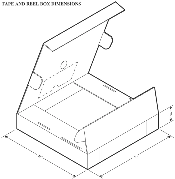
*All dimensions are nominal
| Device | Package Type | Package Drawing | Pins | SPQ | Length (mm) | Width (mm) | Height (mm) |
|---|---|---|---|---|---|---|---|
| TL431ACDBVR | SOT-23 | DBV | 5 | 3000 | 210.0 | 185.0 | 35.0 |
| TL431ACDBVT | SOT-23 | DBV | 5 | 250 | 210.0 | 185.0 | 35.0 |
| TL431ACDBVT | SOT-23 | DBV | 5 | 250 | 210.0 | 185.0 | 35.0 |
| TL431ACDBZR | SOT-23 | DBZ | 3 | 3000 | 210.0 | 185.0 | 35.0 |
| TL431ACDBZRG4 | SOT-23 | DBZ | 3 | 3000 | 210.0 | 185.0 | 35.0 |
| TL431ACDBZT | SOT-23 | DBZ | 3 | 250 | 210.0 | 185.0 | 35.0 |
| TL431ACDBZT | SOT-23 | DBZ | 3 | 250 | 210.0 | 185.0 | 35.0 |
| TL431ACDBZTG4 | SOT-23 | DBZ | 3 | 250 | 210.0 | 185.0 | 35.0 |
| TL431ACDCKR | SC70 | DCK | 6 | 3000 | 183.0 | 183.0 | 20.0 |
| TL431ACDCKR | SC70 | DCK | 6 | 3000 | 210.0 | 185.0 | 35.0 |
| TL431ACDR | SOIC | D | 8 | 2500 | 340.5 | 336.1 | 25.0 |
| TL431ACPK | SOT-89 | PK | 3 | 1000 | 190.0 | 190.0 | 30.0 |
| TL431ACPK | SOT-89 | PK | 3 | 1000 | 340.0 | 340.0 | 38.0 |
| TL431ACPSR | SO | PS | 8 | 2000 | 353.0 | 353.0 | 32.0 |
| TL431ACPWR | TSSOP | PW | 8 | 2000 | 353.0 | 353.0 | 32.0 |
| TL431AIDBVR | SOT-23 | DBV | 5 | 3000 | 210.0 | 185.0 | 35.0 |
| TL431AIDBVT | SOT-23 | DBV | 5 | 250 | 210.0 | 185.0 | 35.0 |
| TL431AIDBVT | SOT-23 | DBV | 5 | 250 | 210.0 | 185.0 | 35.0 |
Pack Materials-Page 7
PACKAGE MATERIALS INFORMATION
10-Aug-2026
| Device | Package Type | Package Drawing | Pins | SPQ | Length (mm) | Width (mm) | Height (mm) |
|---|---|---|---|---|---|---|---|
| TL431AIDBZR | SOT-23 | DBZ | 3 | 3000 | 210.0 | 185.0 | 35.0 |
| TL431AIDBZRG4 | SOT-23 | DBZ | 3 | 3000 | 210.0 | 185.0 | 35.0 |
| TL431AIDBZT | SOT-23 | DBZ | 3 | 250 | 210.0 | 185.0 | 35.0 |
| TL431AIDBZT | SOT-23 | DBZ | 3 | 250 | 210.0 | 185.0 | 35.0 |
| TL431AIDBZTG4 | SOT-23 | DBZ | 3 | 250 | 210.0 | 185.0 | 35.0 |
| TL431AIDCKR | SC70 | DCK | 6 | 3000 | 210.0 | 185.0 | 35.0 |
| TL431AIDCKR | SC70 | DCK | 6 | 3000 | 200.0 | 183.0 | 25.0 |
| TL431AIDCKRG4 | SC70 | DCK | 6 | 3000 | 200.0 | 183.0 | 25.0 |
| TL431AIDCKT | SC70 | DCK | 6 | 250 | 200.0 | 183.0 | 25.0 |
| TL431AIDCKT | SC70 | DCK | 6 | 250 | 210.0 | 185.0 | 35.0 |
| TL431AIDR | SOIC | D | 8 | 2500 | 353.0 | 353.0 | 32.0 |
| TL431AIPK | SOT-89 | PK | 3 | 1000 | 190.0 | 190.0 | 30.0 |
| TL431AIPK | SOT-89 | PK | 3 | 1000 | 340.0 | 340.0 | 38.0 |
| TL431AQDBVR | SOT-23 | DBV | 5 | 3000 | 210.0 | 185.0 | 35.0 |
| TL431AQDBVT | SOT-23 | DBV | 5 | 250 | 210.0 | 185.0 | 35.0 |
| TL431AQDBZR | SOT-23 | DBZ | 3 | 3000 | 210.0 | 185.0 | 35.0 |
| TL431AQDBZRG4 | SOT-23 | DBZ | 3 | 3000 | 210.0 | 185.0 | 35.0 |
| TL431AQDBZT | SOT-23 | DBZ | 3 | 250 | 210.0 | 185.0 | 35.0 |
| TL431AQDBZT | SOT-23 | DBZ | 3 | 250 | 210.0 | 185.0 | 35.0 |
| TL431AQDBZTG4 | SOT-23 | DBZ | 3 | 250 | 210.0 | 185.0 | 35.0 |
| TL431AQDCKR | SC70 | DCK | 6 | 3000 | 200.0 | 183.0 | 25.0 |
| TL431AQDCKR | SC70 | DCK | 6 | 3000 | 210.0 | 185.0 | 35.0 |
| TL431AQDCKT | SC70 | DCK | 6 | 250 | 200.0 | 183.0 | 25.0 |
| TL431AQDCKT | SC70 | DCK | 6 | 250 | 210.0 | 185.0 | 35.0 |
| TL431AQPK | SOT-89 | PK | 3 | 1000 | 340.0 | 340.0 | 38.0 |
| TL431AQPK | SOT-89 | PK | 3 | 1000 | 190.0 | 190.0 | 30.0 |
| TL431BCDBVR | SOT-23 | DBV | 5 | 3000 | 210.0 | 185.0 | 35.0 |
| TL431BCDBVT | SOT-23 | DBV | 5 | 250 | 210.0 | 185.0 | 35.0 |
| TL431BCDBVT | SOT-23 | DBV | 5 | 250 | 210.0 | 185.0 | 35.0 |
| TL431BCDBZR | SOT-23 | DBZ | 3 | 3000 | 210.0 | 185.0 | 35.0 |
| TL431BCDBZRG4 | SOT-23 | DBZ | 3 | 3000 | 210.0 | 185.0 | 35.0 |
| TL431BCDBZT | SOT-23 | DBZ | 3 | 250 | 210.0 | 185.0 | 35.0 |
| TL431BCDBZT | SOT-23 | DBZ | 3 | 250 | 210.0 | 185.0 | 35.0 |
| TL431BCDBZTG4 | SOT-23 | DBZ | 3 | 250 | 210.0 | 185.0 | 35.0 |
| TL431BCDCKR | SC70 | DCK | 6 | 3000 | 200.0 | 183.0 | 25.0 |
| TL431BCDCKR | SC70 | DCK | 6 | 3000 | 210.0 | 185.0 | 35.0 |
| TL431BCDCKT | SC70 | DCK | 6 | 250 | 210.0 | 185.0 | 35.0 |
| TL431BCDCKT | SC70 | DCK | 6 | 250 | 200.0 | 183.0 | 25.0 |
| TL431BCDR | SOIC | D | 8 | 2500 | 353.0 | 353.0 | 32.0 |
| TL431BCDR | SOIC | D | 8 | 2500 | 353.0 | 353.0 | 32.0 |
| TL431BCPK | SOT-89 | PK | 3 | 1000 | 190.0 | 190.0 | 30.0 |
| TL431BCPK | SOT-89 | PK | 3 | 1000 | 340.0 | 340.0 | 38.0 |
| TL431BIDBVR | SOT-23 | DBV | 5 | 3000 | 208.0 | 191.0 | 35.0 |
Pack Materials-Page 8
PACKAGE MATERIALS INFORMATION
10-Aug-2026
| Device | Package Type | Package Drawing | Pins | SPQ | Length (mm) | Width (mm) | Height (mm) |
|---|---|---|---|---|---|---|---|
| TL431BIDBVR | SOT-23 | DBV | 5 | 3000 | 210.0 | 185.0 | 35.0 |
| TL431BIDBVT | SOT-23 | DBV | 5 | 250 | 210.0 | 185.0 | 35.0 |
| TL431BIDBZR | SOT-23 | DBZ | 3 | 3000 | 210.0 | 185.0 | 35.0 |
| TL431BIDBZRG4 | SOT-23 | DBZ | 3 | 3000 | 210.0 | 185.0 | 35.0 |
| TL431BIDBZT | SOT-23 | DBZ | 3 | 250 | 210.0 | 185.0 | 35.0 |
| TL431BIDBZT | SOT-23 | DBZ | 3 | 250 | 210.0 | 185.0 | 35.0 |
| TL431BIDBZTG4 | SOT-23 | DBZ | 3 | 250 | 210.0 | 185.0 | 35.0 |
| TL431BIDCKR | SC70 | DCK | 6 | 3000 | 200.0 | 183.0 | 25.0 |
| TL431BIDCKR | SC70 | DCK | 6 | 3000 | 210.0 | 185.0 | 35.0 |
| TL431BIDCKT | SC70 | DCK | 6 | 250 | 203.0 | 203.0 | 35.0 |
| TL431BIDCKT | SC70 | DCK | 6 | 250 | 210.0 | 185.0 | 35.0 |
| TL431BIDR | SOIC | D | 8 | 2500 | 353.0 | 353.0 | 32.0 |
| TL431BIDR | SOIC | D | 8 | 2500 | 353.0 | 353.0 | 32.0 |
| TL431BIPK | SOT-89 | PK | 3 | 1000 | 190.0 | 190.0 | 30.0 |
| TL431BIPK | SOT-89 | PK | 3 | 1000 | 340.0 | 340.0 | 38.0 |
| TL431BQDBVR | SOT-23 | DBV | 5 | 3000 | 210.0 | 185.0 | 35.0 |
| TL431BQDBVT | SOT-23 | DBV | 5 | 250 | 210.0 | 185.0 | 35.0 |
| TL431BQDBVT | SOT-23 | DBV | 5 | 250 | 210.0 | 185.0 | 35.0 |
| TL431BQDBZR | SOT-23 | DBZ | 3 | 3000 | 210.0 | 185.0 | 35.0 |
| TL431BQDBZRG4 | SOT-23 | DBZ | 3 | 3000 | 210.0 | 185.0 | 35.0 |
| TL431BQDBZT | SOT-23 | DBZ | 3 | 250 | 210.0 | 185.0 | 35.0 |
| TL431BQDBZT | SOT-23 | DBZ | 3 | 250 | 210.0 | 185.0 | 35.0 |
| TL431BQDBZTG4 | SOT-23 | DBZ | 3 | 250 | 210.0 | 185.0 | 35.0 |
| TL431BQDCKR | SC70 | DCK | 6 | 3000 | 200.0 | 183.0 | 25.0 |
| TL431BQDCKR | SC70 | DCK | 6 | 3000 | 210.0 | 185.0 | 35.0 |
| TL431BQDCKT | SC70 | DCK | 6 | 250 | 210.0 | 185.0 | 35.0 |
| TL431BQDCKT | SC70 | DCK | 6 | 250 | 203.0 | 203.0 | 35.0 |
| TL431BQDR | SOIC | D | 8 | 2500 | 353.0 | 353.0 | 32.0 |
| TL431BQDR | SOIC | D | 8 | 2500 | 340.5 | 336.1 | 25.0 |
| TL431BQPK | SOT-89 | PK | 3 | 1000 | 190.0 | 190.0 | 30.0 |
| TL431CDBVR | SOT-23 | DBV | 5 | 3000 | 208.0 | 191.0 | 35.0 |
| TL431CDBVR | SOT-23 | DBV | 5 | 3000 | 210.0 | 185.0 | 35.0 |
| TL431CDBVT | SOT-23 | DBV | 5 | 250 | 210.0 | 185.0 | 35.0 |
| TL431CDBZR | SOT-23 | DBZ | 3 | 3000 | 210.0 | 185.0 | 35.0 |
| TL431CDBZRG4 | SOT-23 | DBZ | 3 | 3000 | 210.0 | 185.0 | 35.0 |
| TL431CDBZT | SOT-23 | DBZ | 3 | 250 | 210.0 | 185.0 | 35.0 |
| TL431CDBZT | SOT-23 | DBZ | 3 | 250 | 210.0 | 185.0 | 35.0 |
| TL431CDBZTG4 | SOT-23 | DBZ | 3 | 250 | 210.0 | 185.0 | 35.0 |
| TL431CDR | SOIC | D | 8 | 2500 | 340.5 | 338.1 | 20.6 |
| TL431CDR-J | SOIC | D | 8 | 2500 | 340.5 | 338.1 | 20.6 |
| TL431CPK | SOT-89 | PK | 3 | 1000 | 190.0 | 190.0 | 30.0 |
| TL431CPK | SOT-89 | PK | 3 | 1000 | 340.0 | 340.0 | 38.0 |
| TL431CPKE6 | SOT-89 | PK | 3 | 1000 | 182.0 | 182.0 | 20.0 |
Pack Materials-Page 9
PACKAGE MATERIALS INFORMATION
10-Aug-2026
| Device | Package Type | Package Drawing | Pins | SPQ | Length (mm) | Width (mm) | Height (mm) |
|---|---|---|---|---|---|---|---|
| TL431IDBVR | SOT-23 | DBV | 5 | 3000 | 210.0 | 185.0 | 35.0 |
| TL431IDBVT | SOT-23 | DBV | 5 | 250 | 210.0 | 185.0 | 35.0 |
| TL431IDBZR | SOT-23 | DBZ | 3 | 3000 | 210.0 | 185.0 | 35.0 |
| TL431IDBZRG4 | SOT-23 | DBZ | 3 | 3000 | 210.0 | 185.0 | 35.0 |
| TL431IDBZT | SOT-23 | DBZ | 3 | 250 | 210.0 | 185.0 | 35.0 |
| TL431IDBZT | SOT-23 | DBZ | 3 | 250 | 210.0 | 185.0 | 35.0 |
| TL431IDBZTG4 | SOT-23 | DBZ | 3 | 250 | 210.0 | 185.0 | 35.0 |
| TL431IDR | SOIC | D | 8 | 2500 | 353.0 | 353.0 | 32.0 |
| TL431IPK | SOT-89 | PK | 3 | 1000 | 190.0 | 190.0 | 30.0 |
| TL431IPK | SOT-89 | PK | 3 | 1000 | 340.0 | 340.0 | 38.0 |
| TL431QDBVR | SOT-23 | DBV | 5 | 3000 | 210.0 | 185.0 | 35.0 |
| TL431QDBVT | SOT-23 | DBV | 5 | 250 | 210.0 | 185.0 | 35.0 |
| TL431QDBZR | SOT-23 | DBZ | 3 | 3000 | 210.0 | 185.0 | 35.0 |
| TL431QDBZRG4 | SOT-23 | DBZ | 3 | 3000 | 210.0 | 185.0 | 35.0 |
| TL431QDBZT | SOT-23 | DBZ | 3 | 250 | 210.0 | 185.0 | 35.0 |
| TL431QDBZT | SOT-23 | DBZ | 3 | 250 | 210.0 | 185.0 | 35.0 |
| TL431QDBZTG4 | SOT-23 | DBZ | 3 | 250 | 210.0 | 185.0 | 35.0 |
| TL431QDCKR | SC70 | DCK | 6 | 3000 | 203.0 | 203.0 | 35.0 |
| TL431QDCKR | SC70 | DCK | 6 | 3000 | 210.0 | 185.0 | 35.0 |
| TL431QDCKT | SC70 | DCK | 6 | 250 | 203.0 | 203.0 | 35.0 |
| TL431QDCKT | SC70 | DCK | 6 | 250 | 210.0 | 185.0 | 35.0 |
| TL431QDR | SOIC | D | 8 | 2500 | 353.0 | 353.0 | 32.0 |
| TL431QDR | SOIC | D | 8 | 2500 | 353.0 | 353.0 | 32.0 |
| TL431QPK | SOT-89 | PK | 3 | 1000 | 190.0 | 190.0 | 30.0 |
| TL432ACDBVR | SOT-23 | DBV | 5 | 3000 | 210.0 | 185.0 | 35.0 |
| TL432ACDBVR | SOT-23 | DBV | 5 | 3000 | 210.0 | 185.0 | 35.0 |
| TL432ACDBZR | SOT-23 | DBZ | 3 | 3000 | 210.0 | 185.0 | 35.0 |
| TL432ACDBZR | SOT-23 | DBZ | 3 | 3000 | 210.0 | 185.0 | 35.0 |
| TL432ACDBZRG4 | SOT-23 | DBZ | 3 | 3000 | 210.0 | 185.0 | 35.0 |
| TL432ACDBZT | SOT-23 | DBZ | 3 | 250 | 210.0 | 185.0 | 35.0 |
| TL432ACDBZT | SOT-23 | DBZ | 3 | 250 | 210.0 | 185.0 | 35.0 |
| TL432ACDBZTG4 | SOT-23 | DBZ | 3 | 250 | 210.0 | 185.0 | 35.0 |
| TL432AIDBVR | SOT-23 | DBV | 5 | 3000 | 210.0 | 185.0 | 35.0 |
| TL432AIDBZR | SOT-23 | DBZ | 3 | 3000 | 210.0 | 185.0 | 35.0 |
| TL432AIDBZRG4 | SOT-23 | DBZ | 3 | 3000 | 210.0 | 185.0 | 35.0 |
| TL432AIDBZT | SOT-23 | DBZ | 3 | 250 | 210.0 | 185.0 | 35.0 |
| TL432AIDBZT | SOT-23 | DBZ | 3 | 250 | 210.0 | 185.0 | 35.0 |
| TL432AIDBZTG4 | SOT-23 | DBZ | 3 | 250 | 210.0 | 185.0 | 35.0 |
| TL432AIPK | SOT-89 | PK | 3 | 1000 | 190.0 | 190.0 | 30.0 |
| TL432AIPK | SOT-89 | PK | 3 | 1000 | 340.0 | 340.0 | 38.0 |
| TL432AQDBVR | SOT-23 | DBV | 5 | 3000 | 210.0 | 185.0 | 35.0 |
| TL432AQDBVR | SOT-23 | DBV | 5 | 3000 | 210.0 | 185.0 | 35.0 |
| TL432AQDBVT | SOT-23 | DBV | 5 | 250 | 210.0 | 185.0 | 35.0 |
Pack Materials-Page 10
PACKAGE MATERIALS INFORMATION
10-Aug-2026
| Device | Package Type | Package Drawing | Pins | SPQ | Length (mm) | Width (mm) | Height (mm) |
|---|---|---|---|---|---|---|---|
| TL432AQDBVT | SOT-23 | DBV | 5 | 250 | 210.0 | 185.0 | 35.0 |
| TL432AQDBZR | SOT-23 | DBZ | 3 | 3000 | 210.0 | 185.0 | 35.0 |
| TL432AQDBZRG4 | SOT-23 | DBZ | 3 | 3000 | 210.0 | 185.0 | 35.0 |
| TL432AQDBZT | SOT-23 | DBZ | 3 | 250 | 210.0 | 185.0 | 35.0 |
| TL432AQDBZT | SOT-23 | DBZ | 3 | 250 | 210.0 | 185.0 | 35.0 |
| TL432AQDBZTG4 | SOT-23 | DBZ | 3 | 250 | 210.0 | 185.0 | 35.0 |
| TL432AQPK | SOT-89 | PK | 3 | 1000 | 340.0 | 340.0 | 38.0 |
| TL432AQPK | SOT-89 | PK | 3 | 1000 | 190.0 | 190.0 | 30.0 |
| TL432BCDBVR | SOT-23 | DBV | 5 | 3000 | 210.0 | 185.0 | 35.0 |
| TL432BCDBVR | SOT-23 | DBV | 5 | 3000 | 210.0 | 185.0 | 35.0 |
| TL432BCDBZR | SOT-23 | DBZ | 3 | 3000 | 210.0 | 185.0 | 35.0 |
| TL432BCDBZR | SOT-23 | DBZ | 3 | 3000 | 210.0 | 185.0 | 35.0 |
| TL432BCDBZRG4 | SOT-23 | DBZ | 3 | 3000 | 210.0 | 185.0 | 35.0 |
| TL432BCDBZT | SOT-23 | DBZ | 3 | 250 | 210.0 | 185.0 | 35.0 |
| TL432BCDBZT | SOT-23 | DBZ | 3 | 250 | 210.0 | 185.0 | 35.0 |
| TL432BCDBZTG4 | SOT-23 | DBZ | 3 | 250 | 210.0 | 185.0 | 35.0 |
| TL432BCPK | SOT-89 | PK | 3 | 1000 | 190.0 | 190.0 | 30.0 |
| TL432BCPK | SOT-89 | PK | 3 | 1000 | 340.0 | 340.0 | 38.0 |
| TL432BIDBZR | SOT-23 | DBZ | 3 | 3000 | 210.0 | 185.0 | 35.0 |
| TL432BIDBZRG4 | SOT-23 | DBZ | 3 | 3000 | 210.0 | 185.0 | 35.0 |
| TL432BIDBZT | SOT-23 | DBZ | 3 | 250 | 210.0 | 185.0 | 35.0 |
| TL432BIDBZT | SOT-23 | DBZ | 3 | 250 | 210.0 | 185.0 | 35.0 |
| TL432BIDBZTG4 | SOT-23 | DBZ | 3 | 250 | 210.0 | 185.0 | 35.0 |
| TL432BIPK | SOT-89 | PK | 3 | 1000 | 340.0 | 340.0 | 38.0 |
| TL432BIPK | SOT-89 | PK | 3 | 1000 | 190.0 | 190.0 | 30.0 |
| TL432BQDBZR | SOT-23 | DBZ | 3 | 3000 | 210.0 | 185.0 | 35.0 |
| TL432BQDBZR1G4 | SOT-23 | DBZ | 3 | 3000 | 210.0 | 185.0 | 35.0 |
| TL432BQPK | SOT-89 | PK | 3 | 1000 | 340.0 | 340.0 | 38.0 |
| TL432BQPK | SOT-89 | PK | 3 | 1000 | 190.0 | 190.0 | 30.0 |
| TL432CDBVR | SOT-23 | DBV | 5 | 3000 | 210.0 | 185.0 | 35.0 |
| TL432CDBVR | SOT-23 | DBV | 5 | 3000 | 210.0 | 185.0 | 35.0 |
| TL432CDBZR | SOT-23 | DBZ | 3 | 3000 | 210.0 | 185.0 | 35.0 |
| TL432CDBZR | SOT-23 | DBZ | 3 | 3000 | 180.0 | 180.0 | 18.0 |
| TL432CDBZRG4 | SOT-23 | DBZ | 3 | 3000 | 210.0 | 185.0 | 35.0 |
| TL432CPK | SOT-89 | PK | 3 | 1000 | 190.0 | 190.0 | 30.0 |
| TL432CPK | SOT-89 | PK | 3 | 1000 | 340.0 | 340.0 | 38.0 |
| TL432IDBVR | SOT-23 | DBV | 5 | 3000 | 210.0 | 185.0 | 35.0 |
| TL432IDBVR | SOT-23 | DBV | 5 | 3000 | 210.0 | 185.0 | 35.0 |
| TL432IDBZR | SOT-23 | DBZ | 3 | 3000 | 210.0 | 185.0 | 35.0 |
| TL432IDBZR | SOT-23 | DBZ | 3 | 3000 | 210.0 | 185.0 | 35.0 |
| TL432IDBZRG4 | SOT-23 | DBZ | 3 | 3000 | 210.0 | 185.0 | 35.0 |
| TL432IDBZT | SOT-23 | DBZ | 3 | 250 | 210.0 | 185.0 | 35.0 |
| TL432IDBZT | SOT-23 | DBZ | 3 | 250 | 210.0 | 185.0 | 35.0 |
Pack Materials-Page 11
PACKAGE MATERIALS INFORMATION
10-Aug-2026
| Device | Package Type | Package Drawing | Pins | SPQ | Length (mm) | Width (mm) | Height (mm) |
|---|---|---|---|---|---|---|---|
| TL432IDBZTG4 | SOT-23 | DBZ | 3 | 250 | 210.0 | 185.0 | 35.0 |
| TL432IPK | SOT-89 | PK | 3 | 1000 | 190.0 | 190.0 | 30.0 |
| TL432IPK | SOT-89 | PK | 3 | 1000 | 340.0 | 340.0 | 38.0 |
| TL432QDBZR | SOT-23 | DBZ | 3 | 3000 | 210.0 | 185.0 | 35.0 |
| TL432QDBZR | SOT-23 | DBZ | 3 | 3000 | 210.0 | 185.0 | 35.0 |
| TL432QDBZRG4 | SOT-23 | DBZ | 3 | 3000 | 210.0 | 185.0 | 35.0 |
| TL432QPK | SOT-89 | PK | 3 | 1000 | 190.0 | 190.0 | 30.0 |
| TL432QPK | SOT-89 | PK | 3 | 1000 | 340.0 | 340.0 | 38.0 |
Pack Materials-Page 12
PACKAGE MATERIALS INFORMATION
10-Aug-2026
TUBE
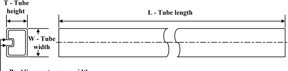
*All dimensions are nominal
| Device | Package Name | Package Type | Pins | SPQ | L (mm) | W (mm) | T (μm) | B (mm) |
|---|---|---|---|---|---|---|---|---|
| TL431ACD | D | SOIC | 8 | 75 | 507 | 8 | 3940 | 4.32 |
| TL431ACD.A | D | SOIC | 8 | 75 | 507 | 8 | 3940 | 4.32 |
| TL431ACP | P | PDIP | 8 | 50 | 506 | 13.97 | 11230 | 4.32 |
| TL431ACP.A | P | PDIP | 8 | 50 | 506 | 13.97 | 11230 | 4.32 |
| TL431AID | D | SOIC | 8 | 75 | 507 | 8 | 3940 | 4.32 |
| TL431AID.A | D | SOIC | 8 | 75 | 507 | 8 | 3940 | 4.32 |
| TL431BCD | D | SOIC | 8 | 75 | 507 | 8 | 3940 | 4.32 |
| TL431BCD.A | D | SOIC | 8 | 75 | 507 | 8 | 3940 | 4.32 |
| TL431BID | D | SOIC | 8 | 75 | 507 | 8 | 3940 | 4.32 |
| TL431BID.A | D | SOIC | 8 | 75 | 507 | 8 | 3940 | 4.32 |
| TL431BQD | D | SOIC | 8 | 75 | 507 | 8 | 3940 | 4.32 |
| TL431BQD.A | D | SOIC | 8 | 75 | 507 | 8 | 3940 | 4.32 |
| TL431CD | D | SOIC | 8 | 75 | 507 | 8 | 3940 | 4.32 |
| TL431CD.A | D | SOIC | 8 | 75 | 507 | 8 | 3940 | 4.32 |
| TL431ID | D | SOIC | 8 | 75 | 507 | 8 | 3940 | 4.32 |
| TL431ID.A | D | SOIC | 8 | 75 | 507 | 8 | 3940 | 4.32 |
| TL431QD | D | SOIC | 8 | 75 | 507 | 8 | 3940 | 4.32 |
| TL431QD.A | D | SOIC | 8 | 75 | 507 | 8 | 3940 | 4.32 |
Pack Materials-Page 13
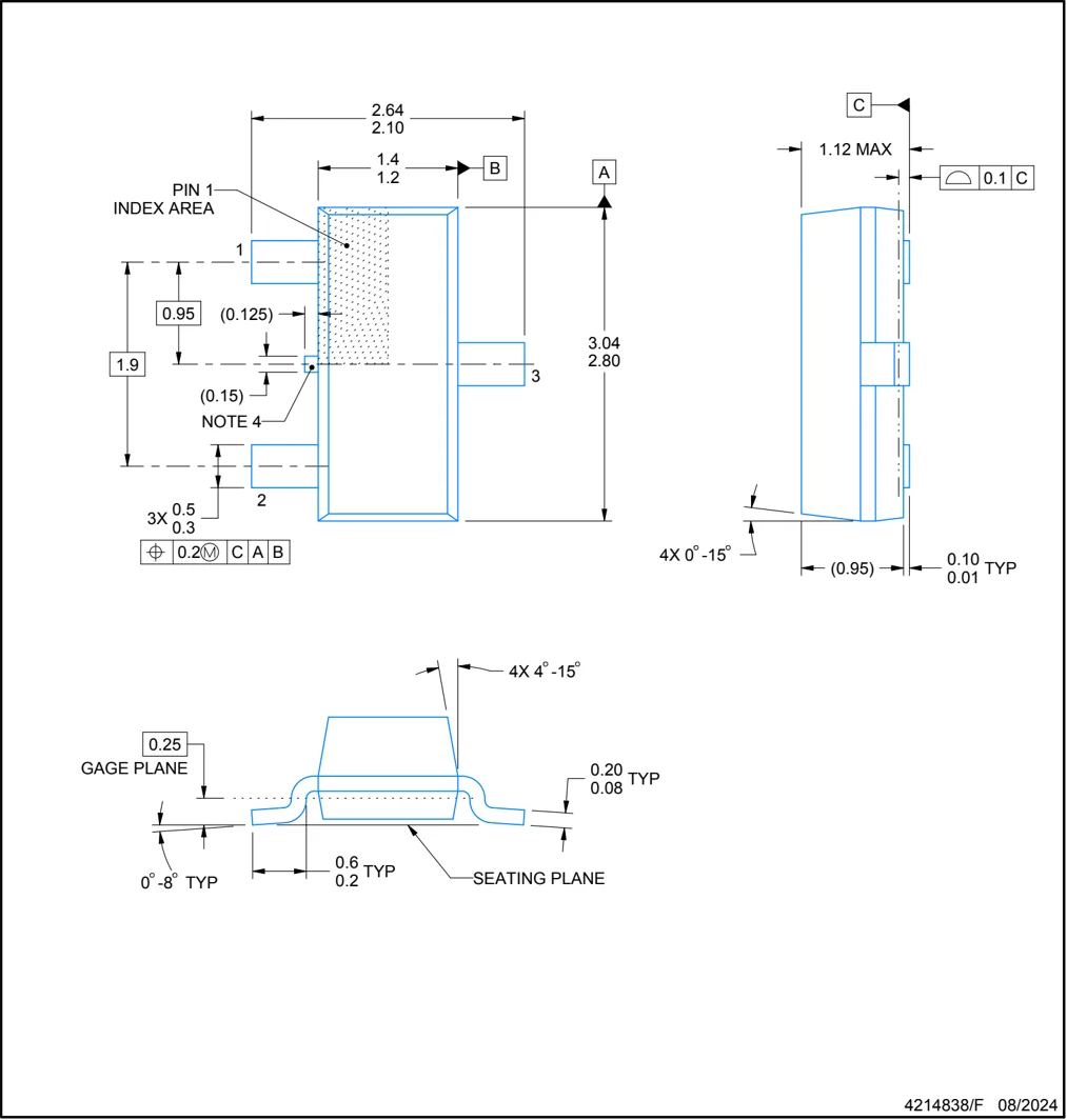
PACKAGE OUTLINE
DBZ0003A
SOT-23 - 1.12 mm max height
SMALL OUTLINE TRANSISTOR

4214838/F 08/2024
NOTES:
- All linear dimensions are in millimeters. Any dimensions in parenthesis are for reference only. Dimensioning and tolerancing per ASME Y14.5M.
- This drawing is subject to change without notice.
- Reference JEDEC registration TO-236, except minimum foot length.
- Support pin may differ or may not be present.
- Body dimensions do not include mold flash, protrusions, or gate burrs. Mold flash, protrusions, or gate burrs shall not exceed 0.25mm per side
TEXAS INSTRUMENTS
EXAMPLE BOARD LAYOUT
DBZ0003A SOT-23 - 1.12 mm max height SMALL OUTLINE TRANSISTOR
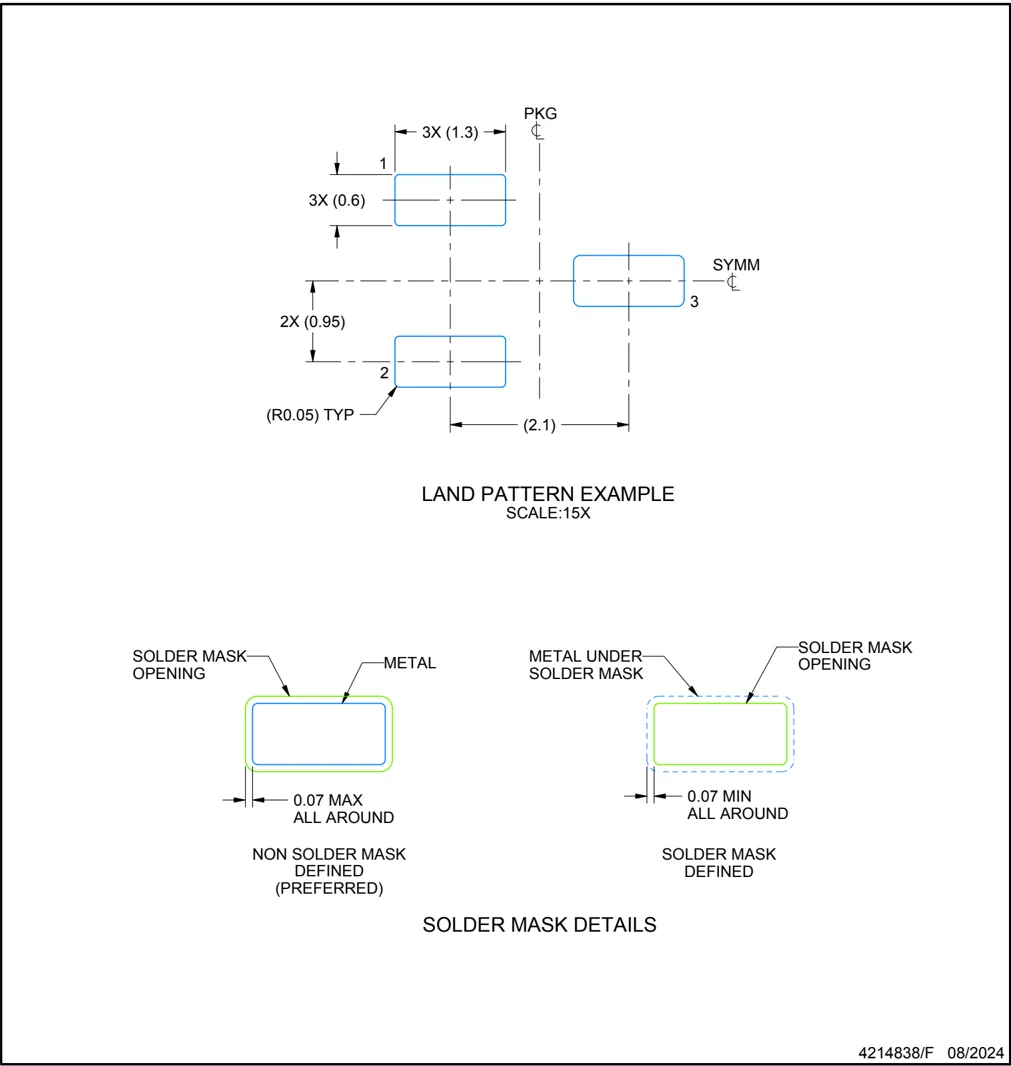
LAND PATTERN EXAMPLE SCALE:15X
SOLDER MASK DETAILS
4214838/F 08/2024
NOTES: (continued)
- Publication IPC-7351 may have alternate designs.
- Solder mask tolerances between and around signal pads can vary based on board fabrication site.
TEXAS INSTRUMENTS
EXAMPLE STENCIL DESIGN
DBZ0003A SOT-23 - 1.12 mm max height SMALL OUTLINE TRANSISTOR
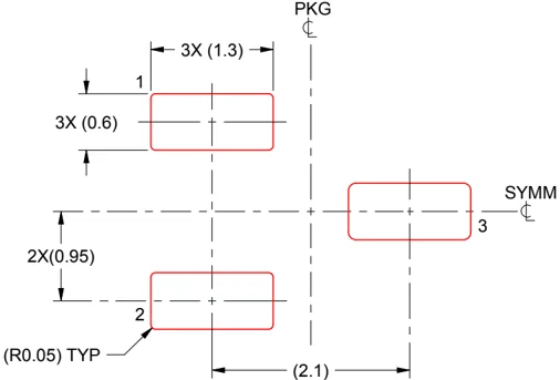
PKG └┴ 3X (1.3) ↓ 1 3X (0.6) ↑ SYMM └┴ 2X(0.95) ↑ 3 2 (R0.05) TYP ↗ (2.1)
SOLDER PASTE EXAMPLE BASED ON 0.125 THICK STENCIL SCALE:15X
4214838/F 08/2024
NOTES: (continued)
- Laser cutting apertures with trapezoidal walls and rounded corners may offer better paste release. IPC-7525 may have alternate design recommendations.
- Board assembly site may have different recommendations for stencil design.
TEXAS INSTRUMENTS
MECHANICAL DATA
PK (R-PSSO-F3) PLASTIC SINGLE-IN-LINE PACKAGE
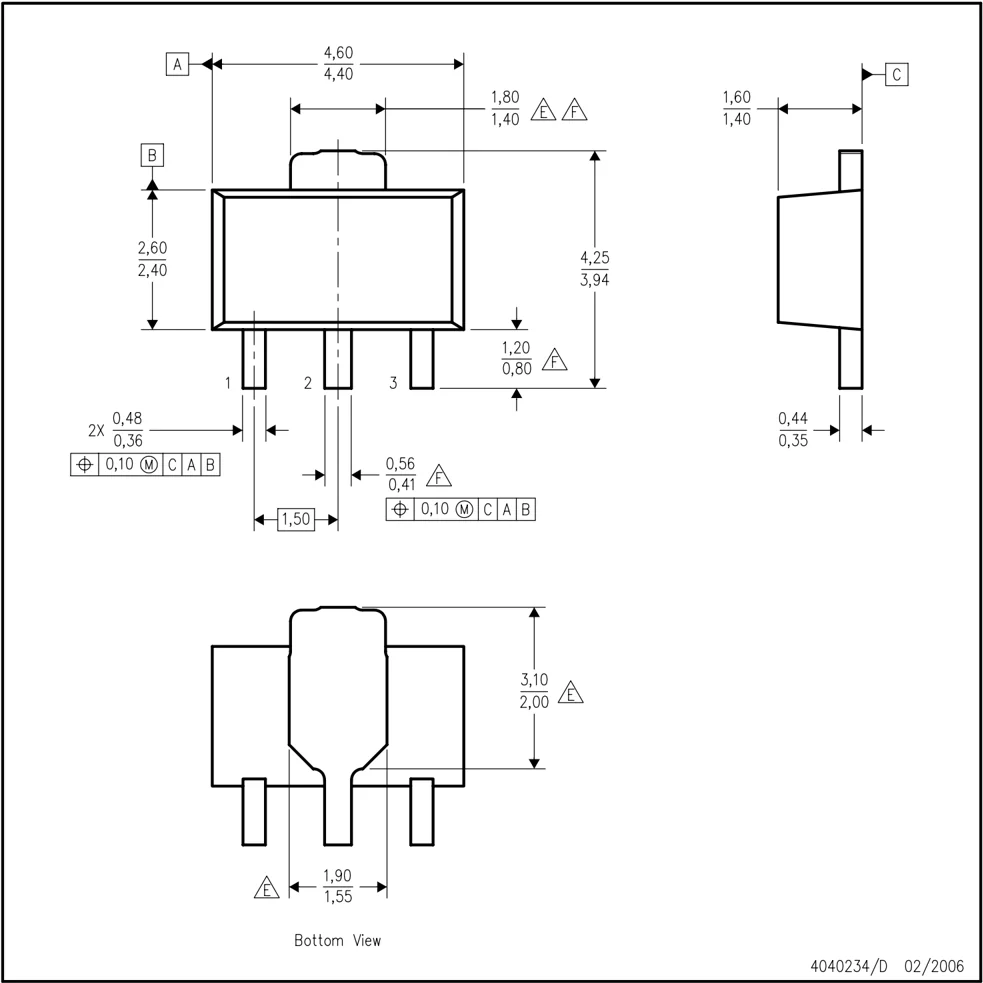
4040234/D 02/2006
NOTES: A. All linear dimensions are in millimeters. Dimensioning and tolerancing per ASME Y14.5M-1994. B. This drawing is subject to change without notice. C. The center lead is in electrical contact with the tab. D. Body dimensions do not include mold flash or protrusion. Mold flash and protrusion not to exceed 0.15 per side. E Thermal pad contour optional within these dimensions. F Falls within JEDEC TO-243 variation AA, except minimum lead length, pin 2 minimum lead width, minimum tab width.
TEXAS INSTRUMENTS

LAND PATTERN
PK (R-PDSO-G3)
 NOTES: A. All linear dimensions are in millimeters.
B. This drawing is subject to change without notice.
C. Publication IPC-7351 is recommended for alternate designs.
D. Laser cutting apertures with trapezoidal walls and also rounding corners will offer better paste release. Customers should contact their board assembly site for stencil design recommendations. Refer to IPC-7525.
E. Customers should contact their board fabrication site for solder mask tolerances between and around signal pads.
4208221/A 09/06

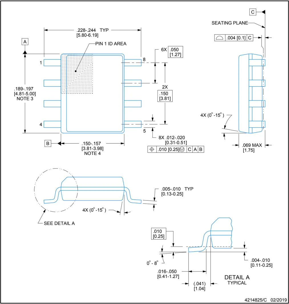
D0008A
PACKAGE OUTLINE
SOIC - 1.75 mm max height
SMALL OUTLINE INTEGRATED CIRCUIT
NOTES:
- Linear dimensions are in inches [millimeters]. Dimensions in parenthesis are for reference only. Controlling dimensions are in inches. Dimensioning and tolerancing per ASME Y14.5M.
- This drawing is subject to change without notice.
- This dimension does not include mold flash, protrusions, or gate burrs. Mold flash, protrusions, or gate burrs shall not exceed .006 [0.15] per side.
- This dimension does not include interlead flash.
- Reference JEDEC registration MS-012, variation AA.
TEXAS INSTRUMENTS
EXAMPLE BOARD LAYOUT
D0008A SOIC - 1.75 mm max height SMALL OUTLINE INTEGRATED CIRCUIT
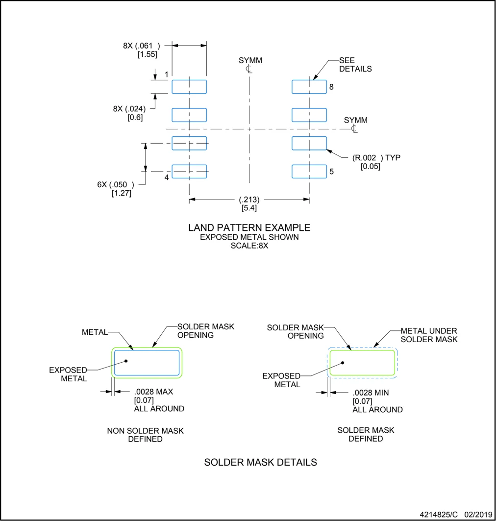
8X (.061 ) [1.55]
SYMM
SEE DETAILS
1
8
8X (.024) [0.6]
SYMM
(R.002 ) TYP [0.05]
4
5
6X (.050 ) [1.27]
(.213) [5.4]
LAND PATTERN EXAMPLE EXPOSED METAL SHOWN SCALE:8X
METAL
SOLDER MASK OPENING
EXPOSED METAL
- 0028 MAX [0.07] ALL AROUND
NON SOLDER MASK DEFINED
SOLDER MASK OPENING
METAL UNDER SOLDER MASK
EXPOSED METAL
- 0028 MIN [0.07] ALL AROUND
SOLDER MASK DEFINED
SOLDER MASK DETAILS
4214825/C 02/2019
NOTES: (continued)
- Publication IPC-7351 may have alternate designs.
- Solder mask tolerances between and around signal pads can vary based on board fabrication site.
TEXAS INSTRUMENTS
EXAMPLE STENCIL DESIGN
D0008A SOIC - 1.75 mm max height SMALL OUTLINE INTEGRATED CIRCUIT
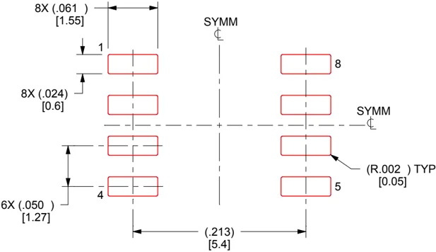
8X (.061 ) [1.55] 1 8X (.024) [0.6] 4 6X (.050 ) [1.27] SYMM ( SYMM ( (R.002 ) TYP [0.05] 8 5 (.213) [5.4]
SOLDER PASTE EXAMPLE BASED ON .005 INCH [0.125 MM] THICK STENCIL SCALE:8X
4214825/C 02/2019
NOTES: (continued)
- Laser cutting apertures with trapezoidal walls and rounded corners may offer better paste release. IPC-7525 may have alternate design recommendations.
- Board assembly site may have different recommendations for stencil design.
TEXAS INSTRUMENTS
MECHANICAL DATA
PS (R-PDSO-G8) PLASTIC SMALL-OUTLINE PACKAGE
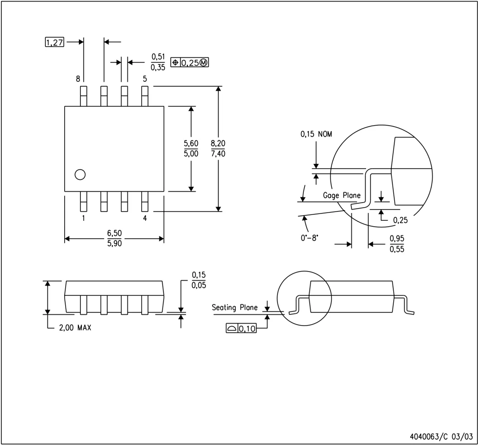
4040063/C 03/03
NOTES: A. All linear dimensions are in millimeters. B. This drawing is subject to change without notice. C. Body dimensions do not include mold flash or protrusion, not to exceed 0,15.
TEXAS INSTRUMENTS

LAND PATTERN DATA
PS (R-PDSO-G8) PLASTIC SMALL OUTLINE
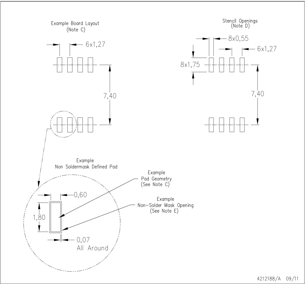
4212188/A 09/11
NOTES: A. All linear dimensions are in millimeters. B. This drawing is subject to change without notice. C. Publication IPC-7351 is recommended for alternate designs. D. Laser cutting apertures with trapezoidal walls and also rounding corners will offer better paste release. Customers should contact their board assembly site for stencil design recommendations. Refer to IPC-7525 for other stencil recommendations. E. Customers should contact their board fabrication site for solder mask tolerances between and around signal pads.

PACKAGE OUTLINE
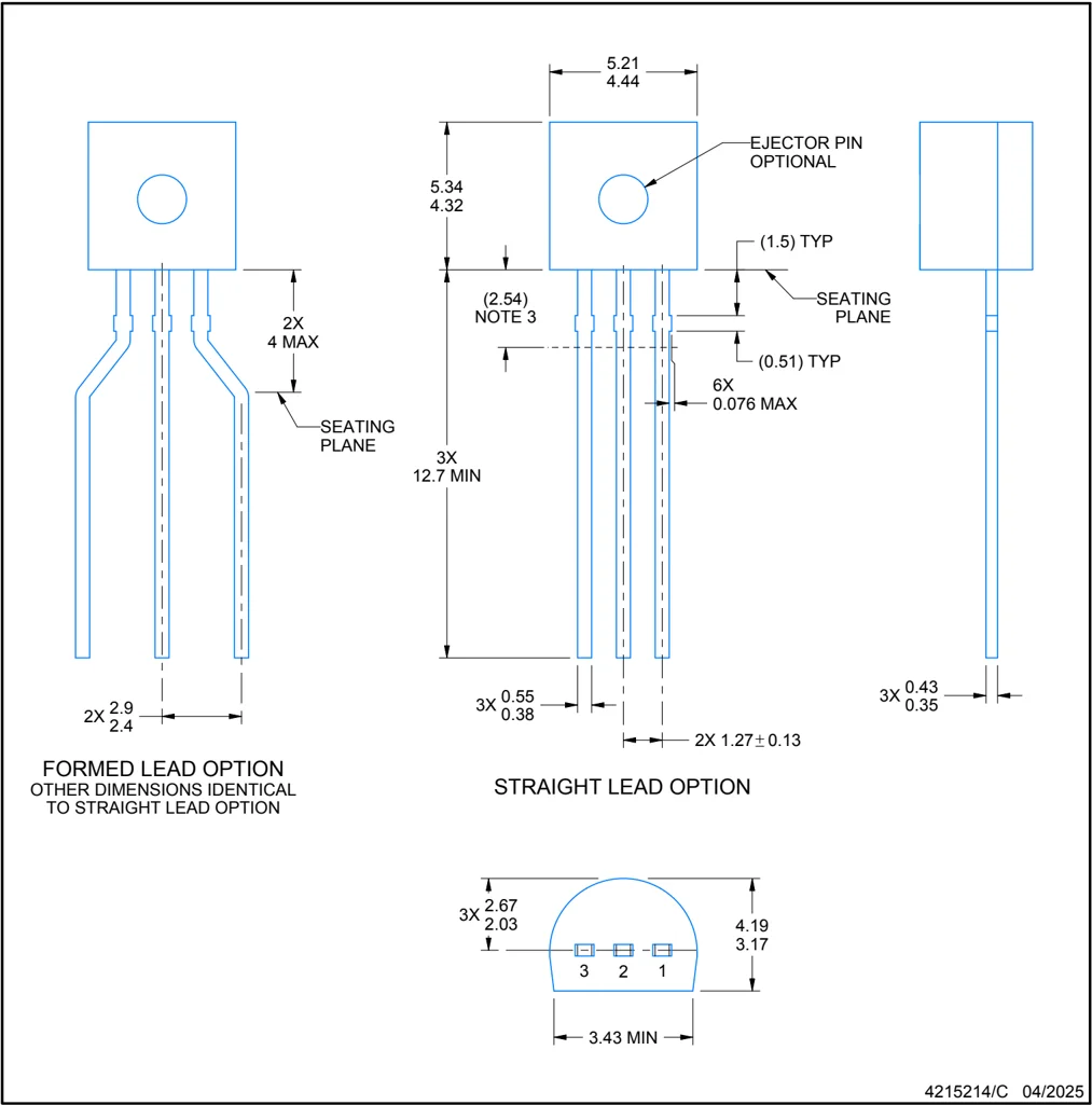
LP0003A
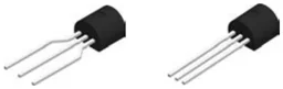
TO-92 - 5.34 mm max height
TO-92
FORMED LEAD OPTION OTHER DIMENSIONS IDENTICAL TO STRAIGHT LEAD OPTION
STRAIGHT LEAD OPTION
4215214/C 04/2025
NOTES:
- All linear dimensions are in millimeters. Any dimensions in parenthesis are for reference only. Dimensioning and tolerancing per ASME Y14.5M.
- This drawing is subject to change without notice.
- Lead dimensions are not controlled within this area.
- Reference JEDEC TO-226, variation AA.
- Shipping method: a. Straight lead option available in bulk pack only. b. Formed lead option available in tape and reel or ammo pack. c. Specific products can be offered in limited combinations of shipping medium and lead options. d. Consult product folder for more information on available options.
TEXAS INSTRUMENTS

EXAMPLE BOARD LAYOUT
LP0003A
TO-92 - 5.34 mm max height TO-92
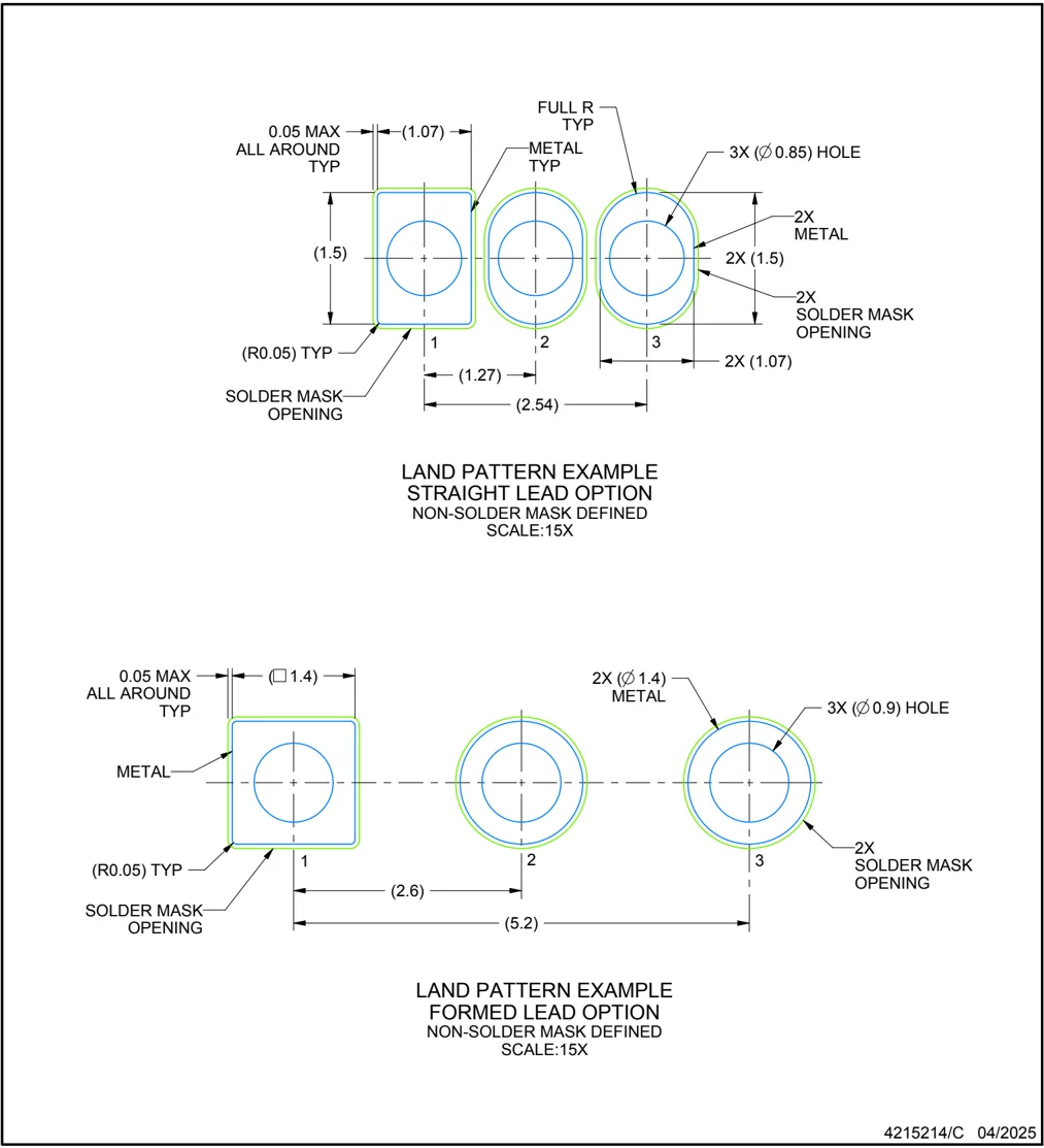
LAND PATTERN EXAMPLE STRAIGHT LEAD OPTION NON-SOLDER MASK DEFINED SCALE:15X

LAND PATTERN EXAMPLE FORMED LEAD OPTION NON-SOLDER MASK DEFINED SCALE:15X
4215214/C 04/2025
TAPE SPECIFICATIONS
LP0003A
TO-92 - 5.34 mm max height
TO-92
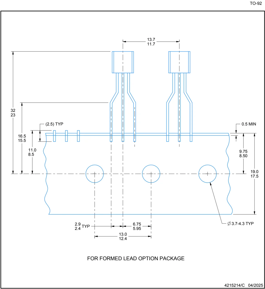
FOR FORMED LEAD OPTION PACKAGE
4215214/C 04/2025

MECHANICAL DATA
P (R-PDIP-T8) PLASTIC DUAL-IN-LINE PACKAGE
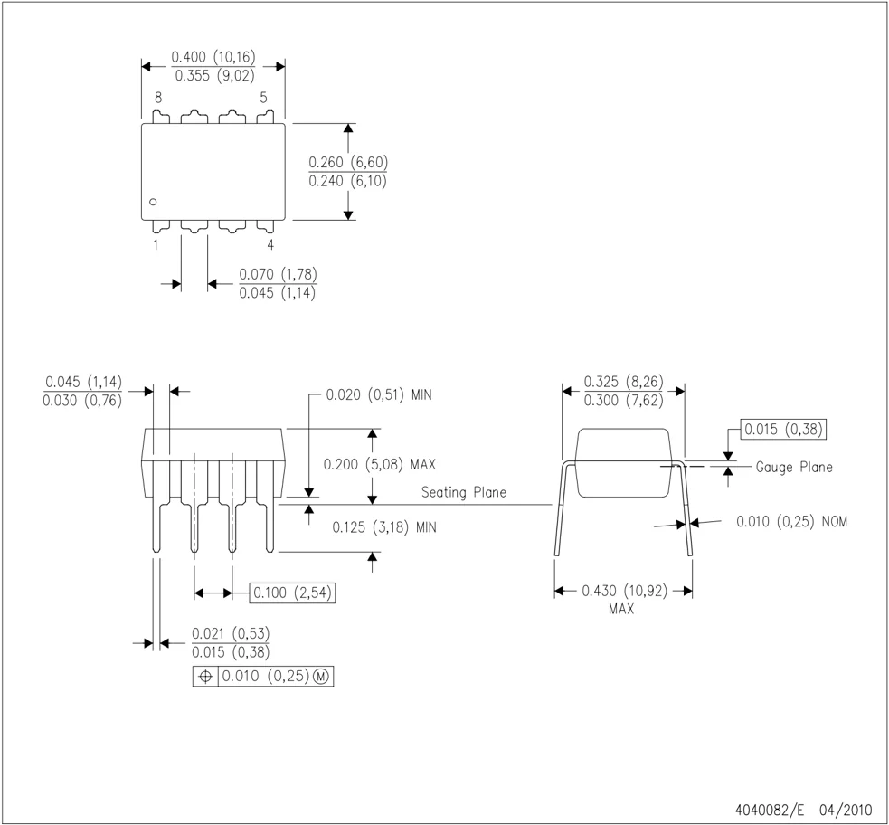
4040082/E 04/2010
NOTES: A. All linear dimensions are in inches (millimeters). B. This drawing is subject to change without notice. C. Falls within JEDEC MS-001 variation BA.
TEXAS INSTRUMENTS

PACKAGE OUTLINE
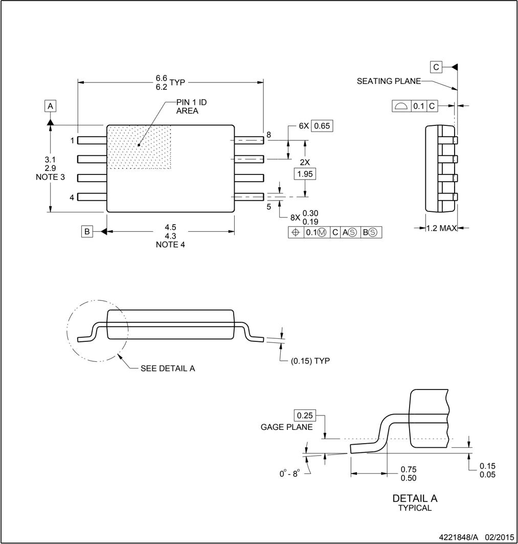
PW0008A
TSSOP - 1.2 mm max height
SMALL OUTLINE PACKAGE
4221848/A 02/2015
NOTES:
- All linear dimensions are in millimeters. Any dimensions in parenthesis are for reference only. Dimensioning and tolerancing per ASME Y14.5M.
- This drawing is subject to change without notice.
- This dimension does not include mold flash, protrusions, or gate burrs. Mold flash, protrusions, or gate burrs shall not exceed 0.15 mm per side.
- This dimension does not include interlead flash. Interlead flash shall not exceed 0.25 mm per side.
- Reference JEDEC registration MO-153, variation AA.
TEXAS INSTRUMENTS

EXAMPLE BOARD LAYOUT
PW0008A
TSSOP - 1.2 mm max height
SMALL OUTLINE PACKAGE
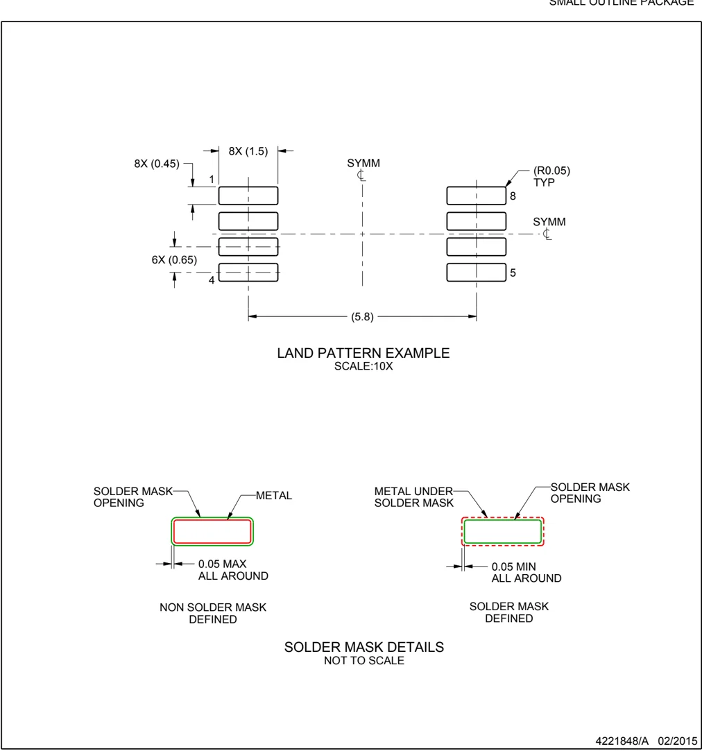
LAND PATTERN EXAMPLE SCALE:10X
SOLDER MASK DETAILS NOT TO SCALE
4221848/A 02/2015
NOTES: (continued) 6. Publication IPC-7351 may have alternate designs. 7. Solder mask tolerances between and around signal pads can vary based on board fabrication site.
TEXAS INSTRUMENTS

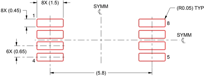
EXAMPLE STENCIL DESIGN
PW0008A TSSOP - 1.2 mm max height SMALL OUTLINE PACKAGE

4221848/A 02/2015
NOTES: (continued)
- Laser cutting apertures with trapezoidal walls and rounded corners may offer better paste release. IPC-7525 may have alternate design recommendations.
- Board assembly site may have different recommendations for stencil design.
TEXAS INSTRUMENTS
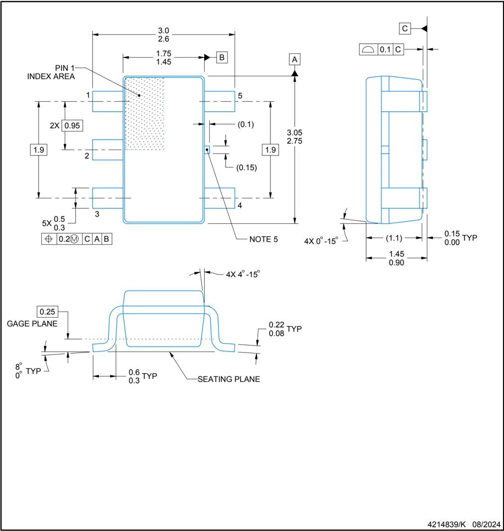
PACKAGE OUTLINE
DBV0005A
SOT-23 - 1.45 mm max height
SMALL OUTLINE TRANSISTOR

4214839/K 08/2024
NOTES:
- All linear dimensions are in millimeters. Any dimensions in parenthesis are for reference only. Dimensioning and tolerancing per ASME Y14.5M.
- This drawing is subject to change without notice.
- Reference JEDEC MO-178.
- Body dimensions do not include mold flash, protrusions, or gate burrs. Mold flash, protrusions, or gate burrs shall not exceed 0.25 mm per side.
- Support pin may differ or may not be present.
TEXAS INSTRUMENTS
EXAMPLE BOARD LAYOUT
DBV0005A
SOT-23 - 1.45 mm max height
SMALL OUTLINE TRANSISTOR
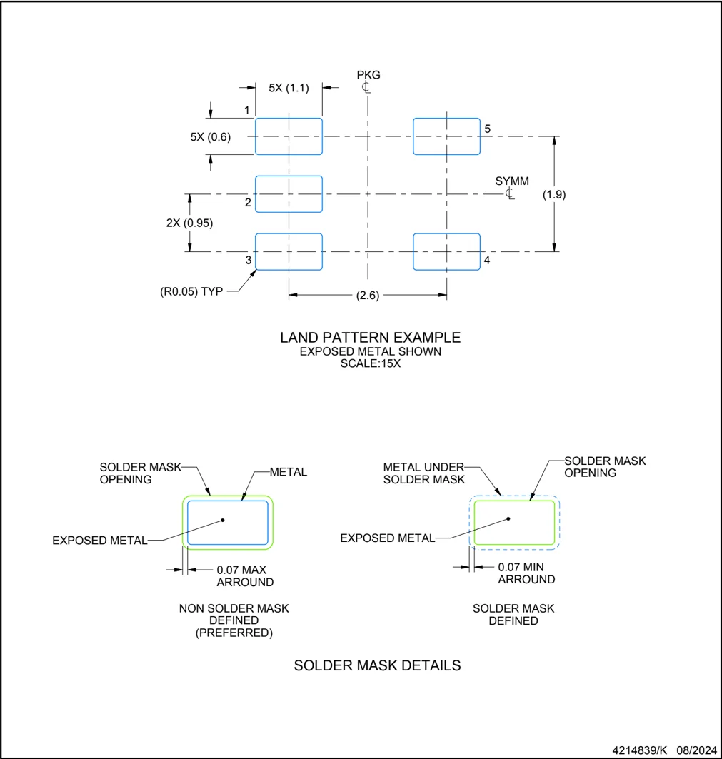
LAND PATTERN EXAMPLE EXPOSED METAL SHOWN SCALE:15X
SOLDER MASK DETAILS
4214839/K 08/2024
NOTES: (continued)
- Publication IPC-7351 may have alternate designs.
- Solder mask tolerances between and around signal pads can vary based on board fabrication site.
TEXAS INSTRUMENTS
EXAMPLE STENCIL DESIGN
DBV0005A SOT-23 - 1.45 mm max height SMALL OUTLINE TRANSISTOR
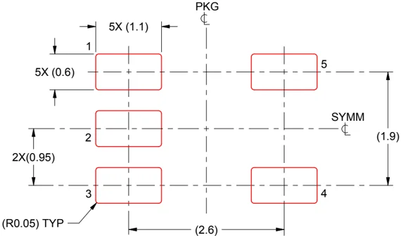
4214839/K 08/2024
NOTES: (continued)
- Laser cutting apertures with trapezoidal walls and rounded corners may offer better paste release. IPC-7525 may have alternate design recommendations.
- Board assembly site may have different recommendations for stencil design.
TEXAS INSTRUMENTS
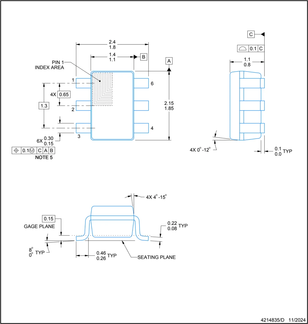
PACKAGE OUTLINE
DCK0006A
SOT - 1.1 max height
SMALL OUTLINE TRANSISTOR

2.4 1.8 1.4 1.1 B A PIN 1 INDEX AREA 1 6 4X 0.65 1.3 2 4 3 2.15 1.85 C 0.1 C 1.1 0.8 6X 0.30 0.15 Φ 0.1 M C A B NOTE 5 4X 0° -12° 0.1 TYP 0.0 0.15 GAGE PLANE 4X 4° -15° 0.22 TYP 0.08 8° 0° TYP 0.46 TYP 0.26 SEATING PLANE
4214835/D 11/2024
NOTES:
- All linear dimensions are in millimeters. Any dimensions in parenthesis are for reference only. Dimensioning and tolerancing per ASME Y14.5M.
- This drawing is subject to change without notice.
- Body dimensions do not include mold flash or protrusion. Mold flash and protrusion shall not exceed 0.15 per side.
- Falls within JEDEC MO-203 variation AB.
TEXAS INSTRUMENTS
EXAMPLE BOARD LAYOUT
DCK0006A
SOT - 1.1 max height
SMALL OUTLINE TRANSISTOR
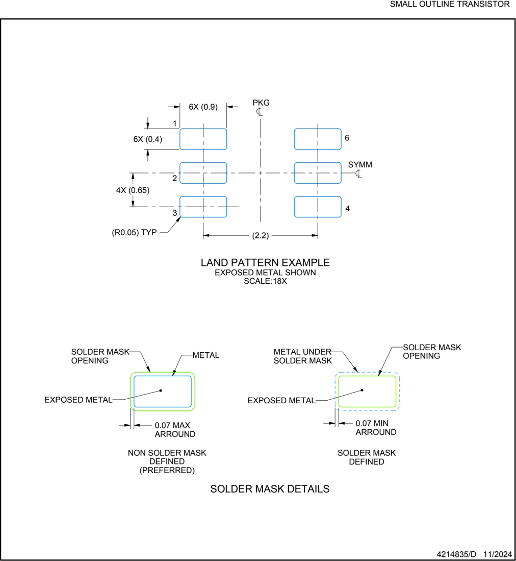
LAND PATTERN EXAMPLE EXPOSED METAL SHOWN SCALE:18X
SOLDER MASK DETAILS
4214835/D 11/2024
NOTES: (continued)
- Publication IPC-7351 may have alternate designs.
- Solder mask tolerances between and around signal pads can vary based on board fabrication site.
TEXAS INSTRUMENTS
EXAMPLE STENCIL DESIGN
DCK0006A
SOT - 1.1 max height
SMALL OUTLINE TRANSISTOR
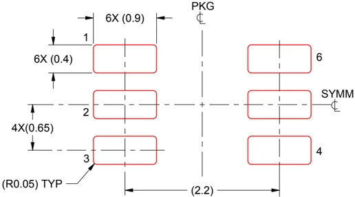
4X(0.65) 6X (0.9) PKG 6X (0.4) 1 2 3 (R0.05) TYP 6 SYMM 4 (2.2)
SOLDER PASTE EXAMPLE BASED ON 0.125 THICK STENCIL SCALE:18X
4214835/D 11/2024
NOTES: (continued)
- Laser cutting apertures with trapezoidal walls and rounded corners may offer better paste release. IPC-7525 may have alternate design recommendations.
- Board assembly site may have different recommendations for stencil design.
TEXAS INSTRUMENTS
IMPORTANT NOTICE AND DISCLAIMER
TI PROVIDES TECHNICAL AND RELIABILITY DATA (INCLUDING DATASHEETS), DESIGN RESOURCES (INCLUDING REFERENCE DESIGNS), APPLICATION OR OTHER DESIGN ADVICE, WEB TOOLS, SAFETY INFORMATION, AND OTHER RESOURCES “AS IS” AND WITH ALL FAULTS, AND DISCLAIMS ALL WARRANTIES, EXPRESS AND IMPLIED, INCLUDING WITHOUT LIMITATION ANY IMPLIED WARRANTIES OF MERCHANTABILITY, FITNESS FOR A PARTICULAR PURPOSE OR NON-INFRINGEMENT OF THIRD PARTY INTELLECTUAL PROPERTY RIGHTS.
These resources are intended for skilled developers designing with TI products. You are solely responsible for (1) selecting the appropriate TI products for your application, (2) designing, validating and testing your application, and (3) ensuring your application meets applicable standards, and any other safety, security, regulatory or other requirements.
These resources are subject to change without notice. TI grants you permission to use these resources only for development of an application that uses the TI products described in the resource. Other reproduction and display of these resources is prohibited. No license is granted to any other TI intellectual property right or to any third party intellectual property right. TI disclaims responsibility for, and you fully indemnify TI and its representatives against any claims, damages, costs, losses, and liabilities arising out of your use of these resources.
TI’s products are provided subject to TI’s Terms of Sale, TI’s General Quality Guidelines, or other applicable terms available either on ti.com or provided in conjunction with such TI products. TI’s provision of these resources does not expand or otherwise alter TI’s applicable warranties or warranty disclaimers for TI products. Unless TI explicitly designates a product as custom or customer-specified, TI products are standard, catalog, general purpose devices.
TI objects to and rejects any additional or different terms you may propose.
Copyright © 2026, Texas Instruments Incorporated
Last updated 10/2025